


 informatics
 electronics
Similar presentations:


")

Digital Electronics. Lecture 12. Semiconductor, Magnetic, and Optical Memory
1.
Semiconductor, Magnetic,and Optical Memory
Lecture 12
Digital Electronics
2.
Course MaterialsAll needed Software and course materials will
be located on Canvas.
◻ Materials that are used in this slides are taken
from the textbook “Digital Electronics A
Practical Approach with VHDL” by William
Kleitz
◻
3.
Semiconductor, Magnetic, andOptical Memory
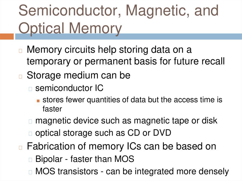
Memory circuits help storing data on a
temporary or permanent basis for future recall
◻ Storage medium can be
◻
◻ semiconductor IC
■ stores fewer quantities of data but the access time is
faster
◻ magnetic device such as magnetic tape or disk
◻ optical storage such as CD or DVD
◻
Fabrication of memory ICs can be based on
◻ Bipolar - faster than MOS
◻ MOS transistors - can be integrated more densely
4.
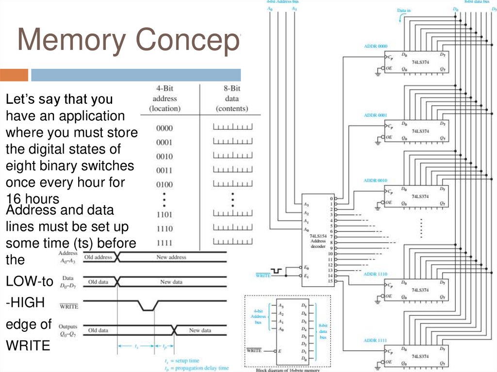
Memory ConceptsLet’s say that you
have an application
where you must store
the digital states of
eight binary switches
once every hour for
16 hours
Address and data
lines must be set up
some time (ts) before
the
LOW-to
-HIGH
edge of
WRITE
5.
Bus ContentionTo avoid a conflict on the data bus the OE
enables would have to be individually
selected at the appropriate time.
To connect the Q0 to Q7 outputs of all 16
memory locations back to the data bus the
grounds on the enables would be removed
and, instead, connected to the output of
another 74LS154 1-of-16 decoder.
6.
Random-Access Memory(RAM)
◻
Used for temporary storage of data and
program instructions (also known as read/write
memory)
◻ magnetic tape - sequential (nonrandom) memory
device
◻ CD player or HDD has random access capability
◻
Static RAMs use flipflops as basic storage
elements
◻ SRAM is faster but more expensive per bit
◻ It is used for the cache memory
◻
Dynamic RAMs use internal capacitors as
7.
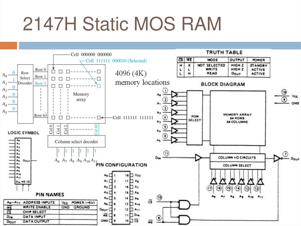
2147H Static MOS RAM4096 (4K)
memory locations
8.
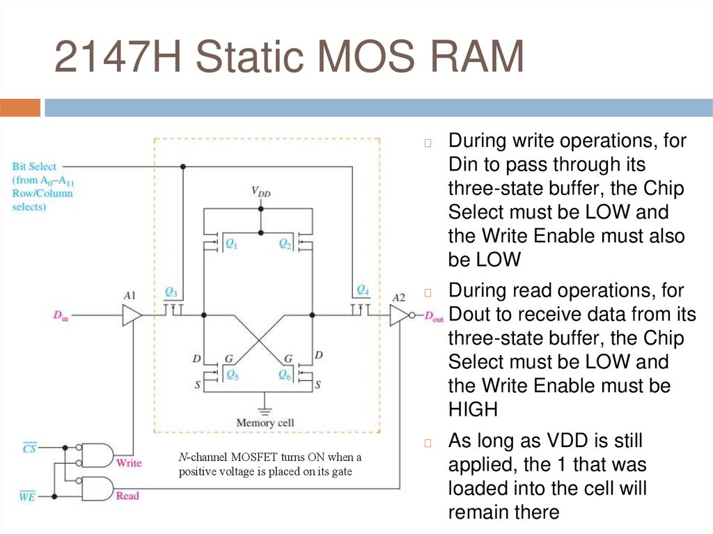
2147H Static MOS RAMN-channel MOSFET turns ON when a
positive voltage is placed on its gate
◻
During write operations, for
Din to pass through its
three-state buffer, the Chip
Select must be LOW and
the Write Enable must also
be LOW
◻
During read operations, for
Dout to receive data from its
three-state buffer, the Chip
Select must be LOW and
the Write Enable must be
HIGH
◻
As long as VDD is still
applied, the 1 that was
loaded into the cell will
remain there
9.
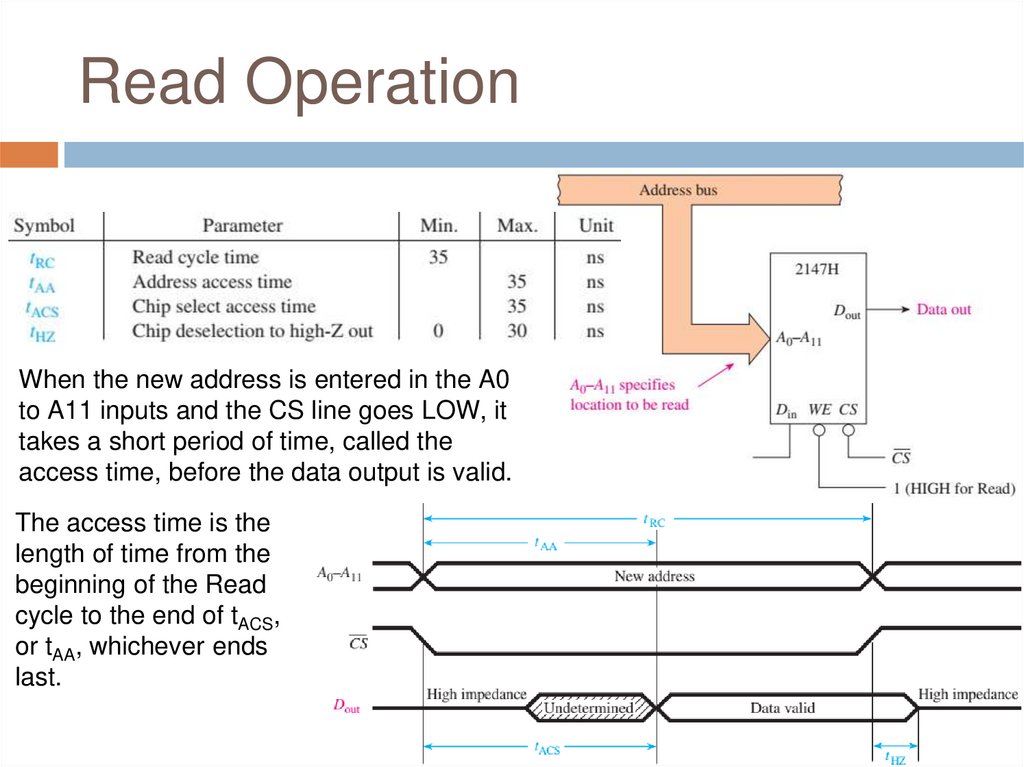
Read OperationWhen the new address is entered in the A0
to A11 inputs and the CS line goes LOW, it
takes a short period of time, called the
access time, before the data output is valid.
The access time is the
length of time from the
beginning of the Read
cycle to the end of tACS,
or tAA, whichever ends
last.
10.
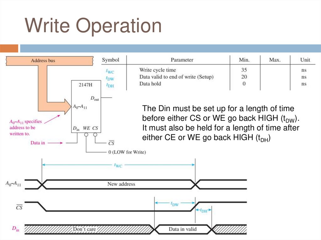
Write OperationThe Din must be set up for a length of time
before either CS or WE go back HIGH (tDW).
It must also be held for a length of time after
either CE or WE go back HIGH (tDH)
11.
Memory ExpansionWith eight 2147s, we have a 4096 x 8
(4K x 8) memory system
◻ WE input determines which internal
three-state buffer is enabled,
connecting either Din or Dout to the
data bus
◻
12.
Modern SRAMs2147H has extremely small
bit size and complexity
◻ suitable choice to learn the
fundamentals of SRAM
circuitry
◻ but it will never find its way
into new designs
◻ Much faster,
denser, lower-power
SRAMs are
available for the
digital designer
◻
13.
Review Questions1.
2.
3.
4.
The _______ (data/address) bus is used to
specify the location of the data stored in a
memory circuit?
Once a memory location is selected, data
travel via the __________ (data/address) bus?
The 2114 memory IC is a 4096 x 1 static
RAM, which means that it has __________
memory locations with __________ data bits
at each location?
To perform a read operation with a 2147H
RAM, CS must be __________ (LOW/HIGH)
14.
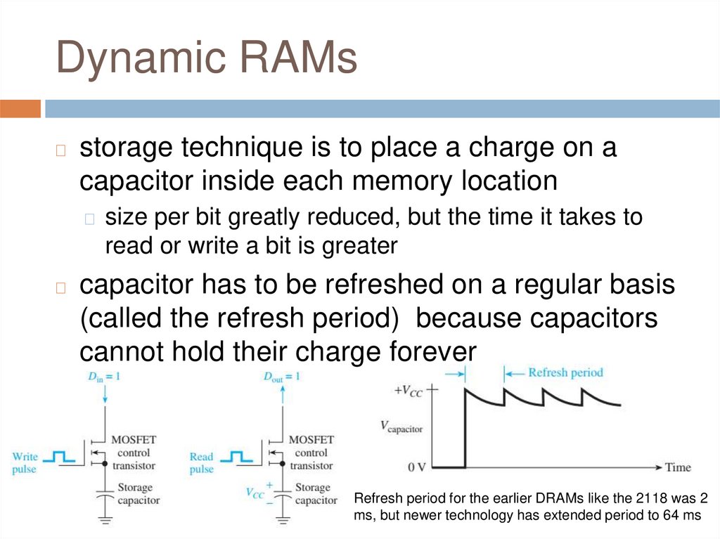
Dynamic RAMs◻
storage technique is to place a charge on a
capacitor inside each memory location
◻ size per bit greatly reduced, but the time it takes to
read or write a bit is greater
◻
capacitor has to be refreshed on a regular basis
(called the refresh period) because capacitors
cannot hold their charge forever
Refresh period for the earlier DRAMs like the 2118 was 2
ms, but newer technology has extended period to 64 ms
15.
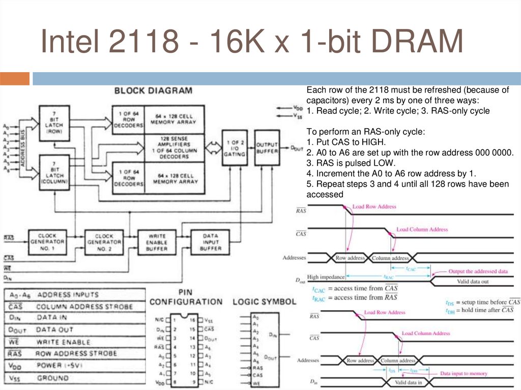
Intel 2118 - 16K x 1-bit DRAMEach row of the 2118 must be refreshed (because of
capacitors) every 2 ms by one of three ways:
1. Read cycle; 2. Write cycle; 3. RAS-only cycle
To perform an RAS-only cycle:
1. Put CAS to HIGH.
2. A0 to A6 are set up with the row address 000 0000.
3. RAS is pulsed LOW.
4. Increment the A0 to A6 row address by 1.
5. Repeat steps 3 and 4 until all 128 rows have been
accessed
16.
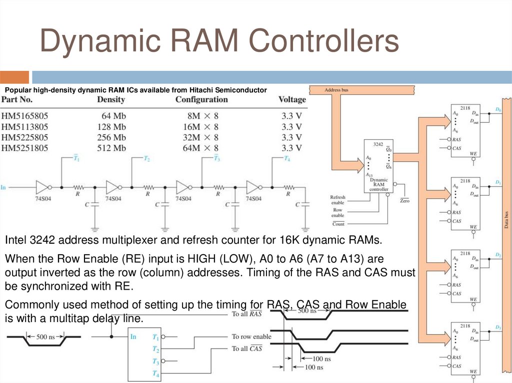
Dynamic RAM ControllersPopular high-density dynamic RAM ICs available from Hitachi Semiconductor
Intel 3242 address multiplexer and refresh counter for 16K dynamic RAMs.
When the Row Enable (RE) input is HIGH (LOW), A0 to A6 (A7 to A13) are
output inverted as the row (column) addresses. Timing of the RAS and CAS must
be synchronized with RE.
Commonly used method of setting up the timing for RAS, CAS and Row Enable
is with a multitap delay line.
17.
Read-Only Memoriesused to store data on a permanent basis
(nonvolatile - do not lose their contents when
power is removed), and are capable of random
access
◻ generally used for read-only operations
◻
◻ not written to after they are initially programmed
◻ there is an erasable variety of ROM called
EPROM
◻ erasable-programmable-read-only memory
◻
to use a ROM the user simply specifies the
correct address to be read and then enables
18.
Mask ROMs VS Fusible-LinkPROMs
◻
Manufacturers make a custom
mask ROM for users who are
absolutely sure of the desired
contents and have a need for at
least 1000 chips
◻
mask is a cover that determines
the permanent logic state to be
formed at each memory location
◻
mask ROMs used for executing
procedures that do not change
such as decoding keyboard or
generate characters for the
display
◻
To avoid the high one-time cost
of producing a custom mask, IC
manufacturers provide user-
19.
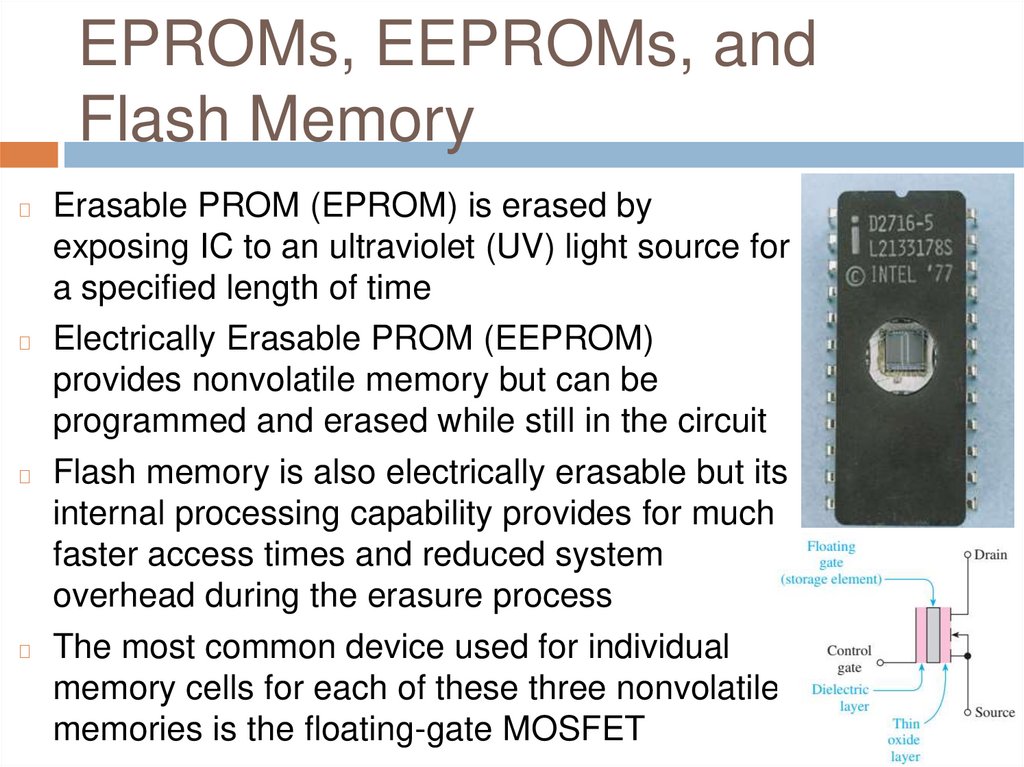
EPROMs, EEPROMs, andFlash Memory
Erasable PROM (EPROM) is erased by
exposing IC to an ultraviolet (UV) light source for
a specified length of time
◻ Electrically Erasable PROM (EEPROM)
provides nonvolatile memory but can be
programmed and erased while still in the circuit
◻ Flash memory is also electrically erasable but its
internal processing capability provides for much
faster access times and reduced system
overhead during the erasure process
◻ The most common device used for individual
memory cells for each of these three nonvolatile
memories is the floating-gate MOSFET
◻
20.
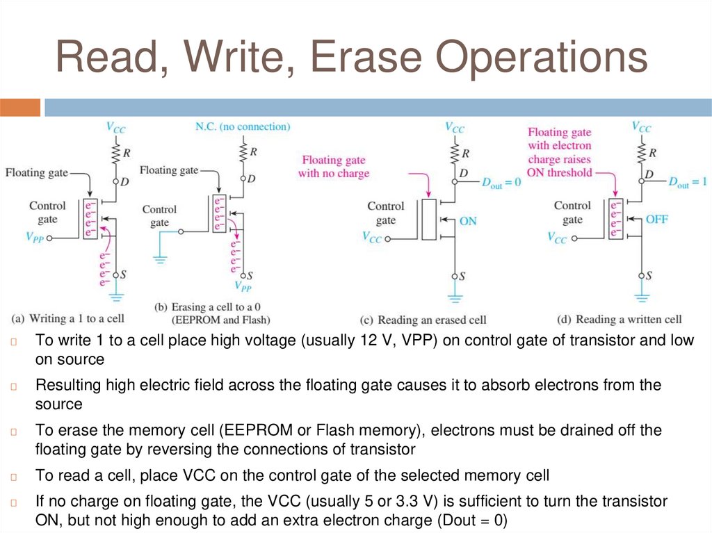
Read, Write, Erase Operations◻
To write 1 to a cell place high voltage (usually 12 V, VPP) on control gate of transistor and low
on source
◻
Resulting high electric field across the floating gate causes it to absorb electrons from the
source
◻
To erase the memory cell (EEPROM or Flash memory), electrons must be drained off the
floating gate by reversing the connections of transistor
◻
To read a cell, place VCC on the control gate of the selected memory cell
◻
If no charge on floating gate, the VCC (usually 5 or 3.3 V) is sufficient to turn the transistor
ON, but not high enough to add an extra electron charge (Dout = 0)
21.
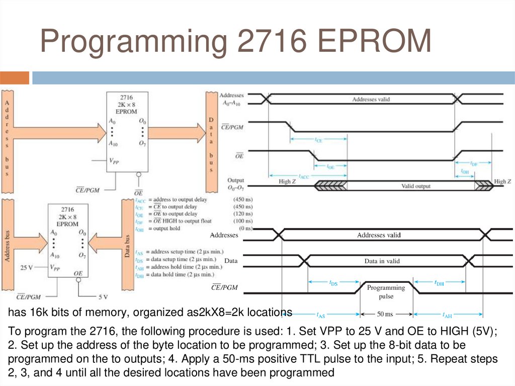
Programming 2716 EPROMhas 16k bits of memory, organized as2kX8=2k locations
To program the 2716, the following procedure is used: 1. Set VPP to 25 V and OE to HIGH (5V);
2. Set up the address of the byte location to be programmed; 3. Set up the 8-bit data to be
programmed on the to outputs; 4. Apply a 50-ms positive TTL pulse to the input; 5. Repeat steps
2, 3, and 4 until all the desired locations have been programmed
22.
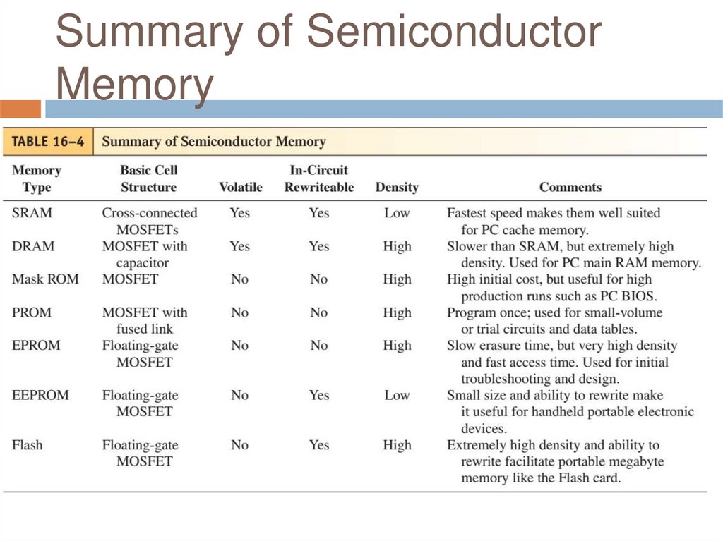
Summary of SemiconductorMemory
23.
Review Questions1.
2.
3.
4.
What is the primary storage medium in a
DRAM memory cell?
What is meant by refreshing a DRAM?
What is meant by the term volatile?
Which of following memory ICs are volatile
and which are nonvolatile?
a) Mask ROM
b) SRAM
c) DRAM
d) EEPROM
24.
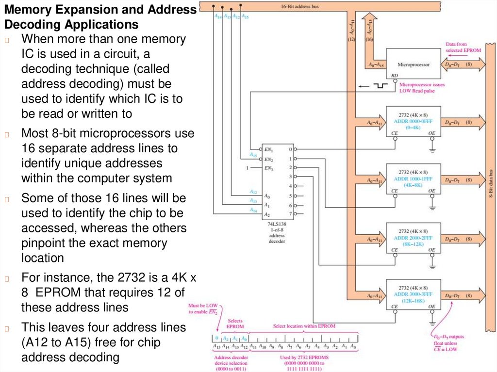
Memory Expansion and AddressDecoding Applications
◻
When more than one memory
IC is used in a circuit, a
decoding technique (called
address decoding) must be
used to identify which IC is to
be read or written to
◻
Most 8-bit microprocessors use
16 separate address lines to
identify unique addresses
within the computer system
◻
Some of those 16 lines will be
used to identify the chip to be
accessed, whereas the others
pinpoint the exact memory
location
◻
For instance, the 2732 is a 4K x
8 EPROM that requires 12 of
these address lines
◻
This leaves four address lines
(A12 to A15) free for chip
address decoding
25.
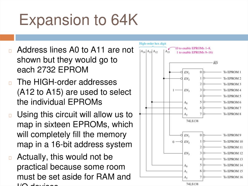
Expansion to 64KAddress lines A0 to A11 are not
shown but they would go to
each 2732 EPROM
◻ The HIGH-order addresses
(A12 to A15) are used to select
the individual EPROMs
◻ Using this circuit will allow us to
map in sixteen EPROMs, which
will completely fill the memory
map in a 16-bit address system
◻ Actually, this would not be
practical because some room
must be set aside for RAM and
◻
26.
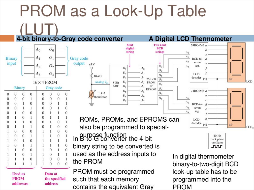
PROM as a Look-Up Table(LUT)
4-bit binary-to-Gray code converter
A Digital LCD Thermometer
ROMs, PROMs, and EPROMS can
also be programmed to specialpurpose function
In B-to-G converter the 4-bit
binary string to be converted is
used as the address inputs to
In digital thermometer
the PROM
binary-to-two-digit BCD
PROM must be programmed
such that each memory
contains the equivalent Gray
look-up table has to be
programmed into the
PROM
27.
Magnetic and Optical Storage◻
most common magnetic and optical memories are more
electromechanical in nature
◻
memory material (containing 1s and 0s) physically spins beneath
a read/write head
they are nonvolatile, providing permanent storage and
retrieval even when power is removed
◻ In the case of magnetic memory, the 1 or 0 is
represented on the magnetic medium as a tiny north–
south or south–north polarity magnet
◻ optical memory differs in that it uses a laser to optically
read the data stored on the medium
◻ An indentation area (called a pit) represents 1, and a
non-pit (called land) represents 0
◻
28.
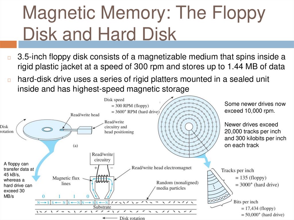
Magnetic Memory: The FloppyDisk and Hard Disk
◻
3.5-inch floppy disk consists of a magnetizable medium that spins inside a
rigid plastic jacket at a speed of 300 rpm and stores up to 1.44 MB of data
◻
hard-disk drive uses a series of rigid platters mounted in a sealed unit
inside and has highest-speed magnetic storage
Some newer drives now
exceed 10,000 rpm.
Newer drives exceed
20,000 tracks per inch
and 300 kilobits per inch
on each track
A floppy can
transfer data at
45 kB/s,
whereas a
hard drive can
exceed 30
MB/s
29.
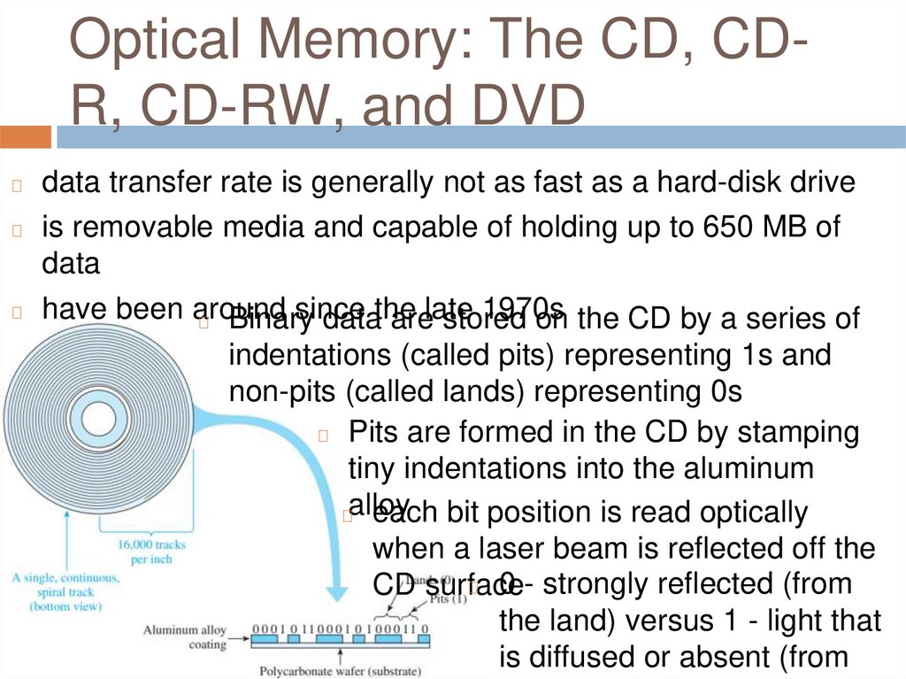
Optical Memory: The CD, CDR, CD-RW, and DVDdata transfer rate is generally not as fast as a hard-disk drive
◻ is removable media and capable of holding up to 650 MB of
data
◻ have been around since the late 1970s
◻ Binary data are stored on the CD by a series of
◻
indentations (called pits) representing 1s and
non-pits (called lands) representing 0s
◻ Pits are formed in the CD by stamping
tiny indentations into the aluminum
◻alloy
each bit position is read optically
when a laser beam is reflected off the
◻ 0 - strongly reflected (from
CD surface
the land) versus 1 - light that
is diffused or absent (from
30.
CD-R, CD-RW, and DVD◻
CD-R make CDs recordable with a photosensitive dye on a
reflective gold layer placed on the bottom of the rigid polycarbonate
wafer
◻
◻
To form a 1, the CD recorder superheats a tiny spot on the dye/gold
layer, changing its composition so that it will not reflect the laser light in
that one spot
CD-RW rewritable type of CD with surface of silver alloy crystalline
structure
converted into a 1 by superheating the specific bit area turning it into
non-reflective state
◻ 1 can be converted back to look like a 0 by reapplying a lower level heat
to that area, which returns the silver alloy back to its crystalline
(reflective) state
◻
◻
DVD (Digital Versatile Disk) offer much higher quality and greater
content
◻ constructed similarly to the CD but have a much higher data capacity,
31.
Some exercisesDesign and sketch an 8-byte memory system using
eight 74LS374s and one 74LS138
◻ Design and sketch a 1K x 8 RAM memory system using
two 2148Hs. (2148Hs are 1K x 4 with WE and CS)
◻ Design and sketch an address decoding scheme for an
8K x 8 EPROM memory system using 2716 EPROMs.
(The 2716 is a 2K x 8 EPROM.)
◻ Design a PROM IC to act like a 3-bit controlled inverter.
Use a 16 x 4 PROM. When A3 is HIGH, the input at A0
to A2 is to be inverted; otherwise, it is not. Build a truth
table showing the 16 possible inputs and the resultant
output at Q0 to Q2 (Q3 is not used).
◻
32.
Q&AAny Questions?