

 informatics
 electronics
Similar presentations:


")


Digital Electronics. Lecture 13. Microprocessor Fundamentals
1.
Microprocessor FundamentalsLecture 13
Digital Electronics
2.
Course MaterialsAll needed Software and course materials will
be located on Canvas.
◻ Materials that are used in this slides are taken
from the textbook “Digital Electronics A
Practical Approach with VHDL” by William
Kleitz
◻
3.
Microprocessor Fundamentals◻
system designer should consider a
microprocessor-based solution whenever an
application involves
◻ making calculations
◻ making decisions based on external stimulus
◻ maintaining memory of past events
◻
microprocessor itself is a general-purpose
device
◻ counting, shifting, etc. are done by software
instructions
◻
making changes to an application can usually
4.
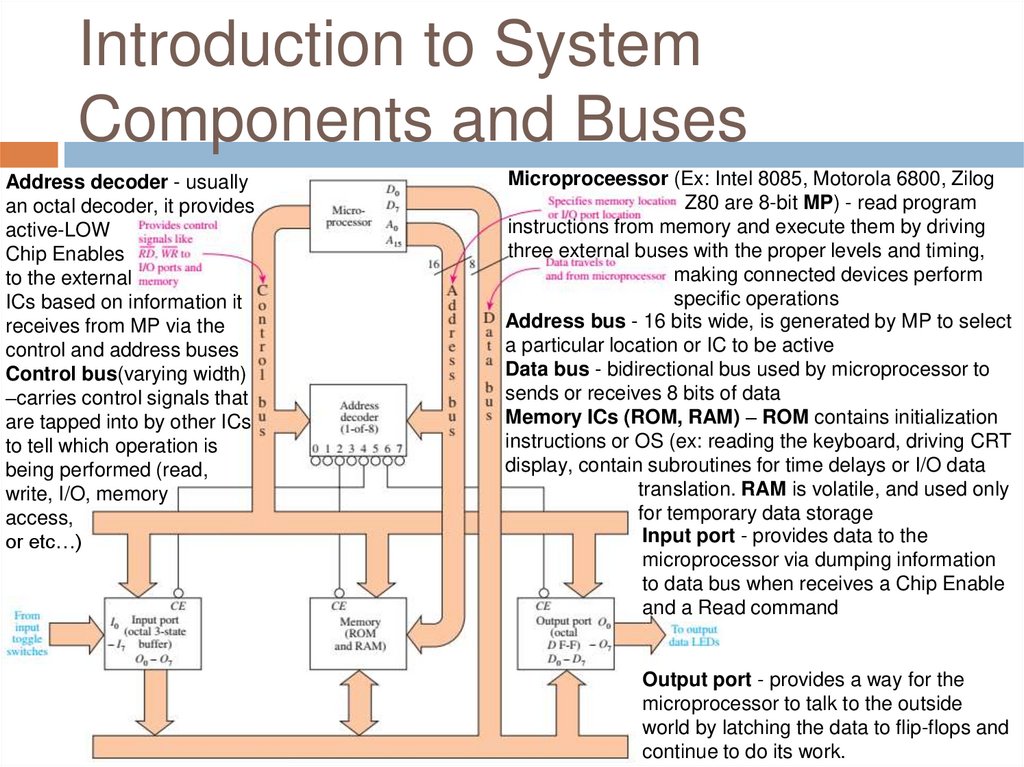
Introduction to SystemComponents and Buses
Address decoder - usually
an octal decoder, it provides
active-LOW
Chip Enables
to the external
ICs based on information it
receives from MP via the
control and address buses
Control bus(varying width)
–carries control signals that
are tapped into by other ICs
to tell which operation is
being performed (read,
write, I/O, memory
access,
or etc…)
Microproceessor (Ex: Intel 8085, Motorola 6800, Zilog
Z80 are 8-bit MP) - read program
instructions from memory and execute them by driving
three external buses with the proper levels and timing,
making connected devices perform
specific operations
Address bus - 16 bits wide, is generated by MP to select
a particular location or IC to be active
Data bus - bidirectional bus used by microprocessor to
sends or receives 8 bits of data
Memory ICs (ROM, RAM) – ROM contains initialization
instructions or OS (ex: reading the keyboard, driving CRT
display, contain subroutines for time delays or I/O data
translation. RAM is volatile, and used only
for temporary data storage
Input port - provides data to the
microprocessor via dumping information
to data bus when receives a Chip Enable
and a Read command
Output port - provides a way for the
microprocessor to talk to the outside
world by latching the data to flip-flops and
continue to do its work.
5.
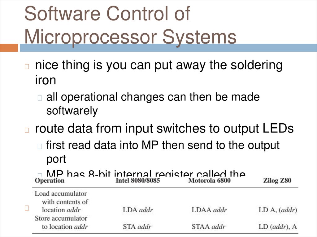
Software Control ofMicroprocessor Systems
◻
nice thing is you can put away the soldering
iron
◻ all operational changes can then be made
softwarely
◻
route data from input switches to output LEDs
◻ first read data into MP then send to the output
port
◻ MP has 8-bit internal register called the
accumulator
◻
Software used to drive microprocessor-based
systems is called assembly language
6.
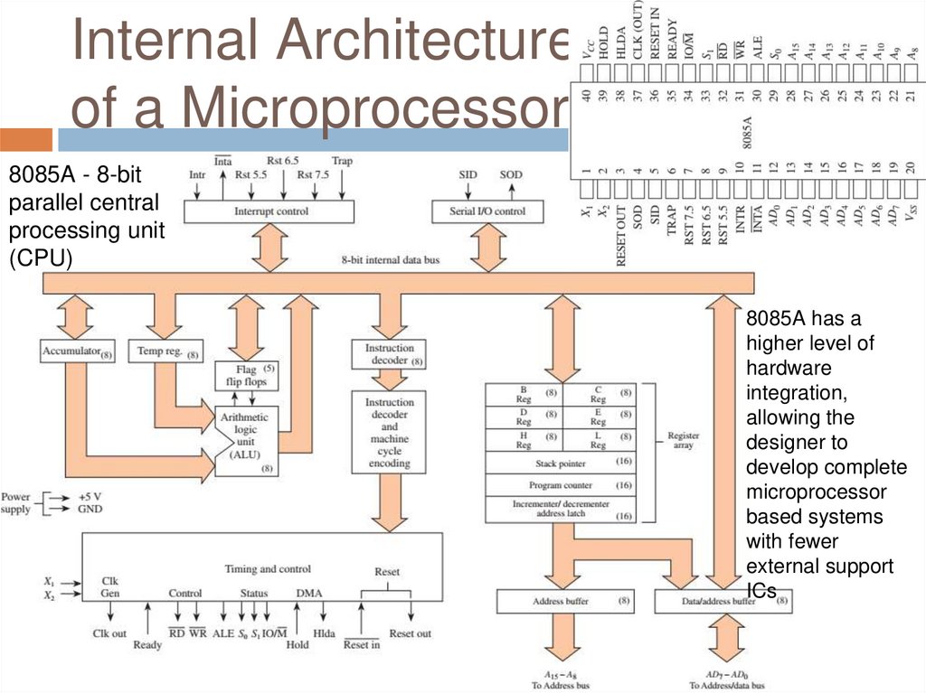
Internal Architectureof a Microprocessor
8085A - 8-bit
parallel central
processing unit
(CPU)
8085A has a
higher level of
hardware
integration,
allowing the
designer to
develop complete
microprocessor
based systems
with fewer
external support
ICs
7.
Processor Operation◻
accumulator and general-purpose registers (B, C, D, E, H, L)
are connected to 8-bit internal data bus to store data
◻ GPR can be used in pairs (B–C, D–E…) to store addresses or 16-bit
data
◻
all arithmetic operations take place in the arithmetic logic unit
(ALU)
accumulator, along with a temporary register, is used as input
◻ output is sent to internal data bus and to five flag flip-flops
◻
flag flip-flops record the status of the arithmetic operation
◻ instruction register and decoder
◻
receive the software instructions from external memory
◻ interpret what is to be done
◻ create the necessary timing and control signals
◻
8.
Processor Operation◻
interrupt control provides way for external digital signal to
interrupt software program while it is executing
◻
by applying proper digital signal on one of interrupt inputs: INTR,
RSTx.x, TRAP
serial communication capabilities are provided via the SID and
SOD I/O pins (Serial Input Data, Serial Output Data)
◻ register array contains the six general-purpose 8-bit registers
and three 16-bit registers required to store addresses
◻ stack pointer stores the address of the last entry on the stack
◻
◻
◻
stack is a data storage area in RAM used by certain microprocessor
operations
program counter contains 16-bit address of the next software
instruction to be executed
9.
Review Questions1.
2.
3.
4.
What are the names of the three buses
associated with microprocessors?
The purpose of the address decoder IC is to
enable two or more of the external ICs to be
active at the same time to speed up
processing. True or false?
Why must the data bus be bidirectional?
The LDA command is used by the
microprocessor to _________ (read/write)
data, and the STA command is used to
_________ (read/write) data?
10.
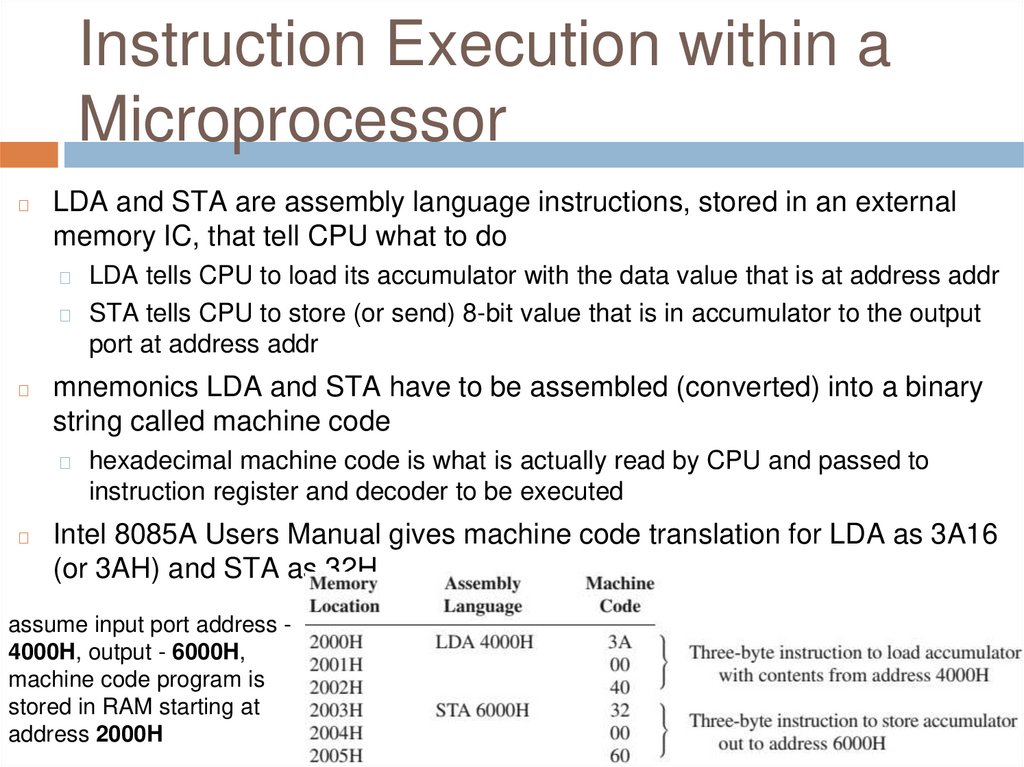
Instruction Execution within aMicroprocessor
◻
LDA and STA are assembly language instructions, stored in an external
memory IC, that tell CPU what to do
LDA tells CPU to load its accumulator with the data value that is at address addr
◻ STA tells CPU to store (or send) 8-bit value that is in accumulator to the output
port at address addr
◻
◻
mnemonics LDA and STA have to be assembled (converted) into a binary
string called machine code
◻
◻
hexadecimal machine code is what is actually read by CPU and passed to
instruction register and decoder to be executed
Intel 8085A Users Manual gives machine code translation for LDA as 3A16
(or 3AH) and STA as 32H
assume input port address 4000H, output - 6000H,
machine code program is
stored in RAM starting at
address 2000H
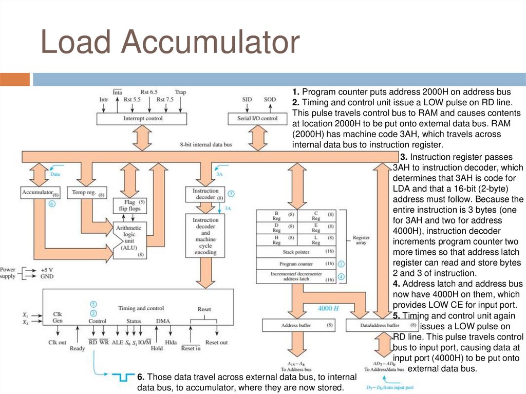
11.
Load Accumulator1. Program counter puts address 2000H on address bus
2. Timing and control unit issue a LOW pulse on RD line.
This pulse travels control bus to RAM and causes contents
at location 2000H to be put onto external data bus. RAM
(2000H) has machine code 3AH, which travels across
internal data bus to instruction register.
3. Instruction register passes
3AH to instruction decoder, which
determines that 3AH is code for
LDA and that a 16-bit (2-byte)
address must follow. Because the
entire instruction is 3 bytes (one
for 3AH and two for address
4000H), instruction decoder
increments program counter two
more times so that address latch
register can read and store bytes
2 and 3 of instruction.
4. Address latch and address bus
now have 4000H on them, which
provides LOW CE for input port.
5. Timing and control unit again
issues a LOW pulse on
RD line. This pulse travels control
bus to input port, causing data at
input port (4000H) to be put onto
external data bus.
6. Those data travel across external data bus, to internal
data bus, to accumulator, where they are now stored.
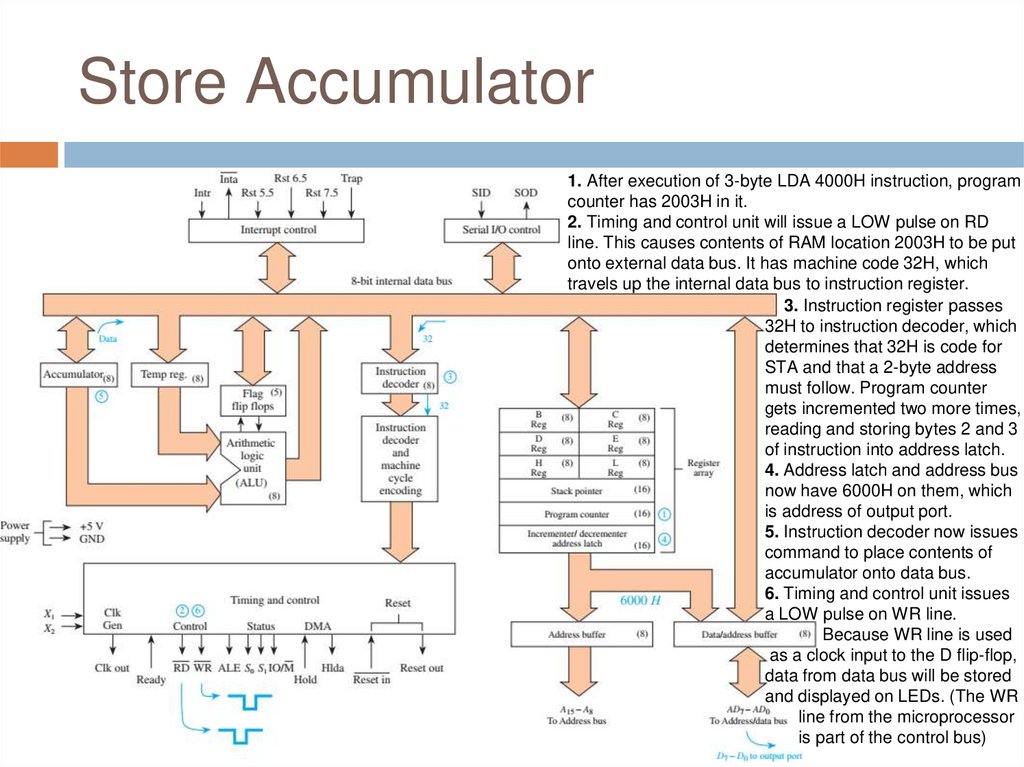
12.
Store Accumulator1. After execution of 3-byte LDA 4000H instruction, program
counter has 2003H in it.
2. Timing and control unit will issue a LOW pulse on RD
line. This causes contents of RAM location 2003H to be put
onto external data bus. It has machine code 32H, which
travels up the internal data bus to instruction register.
3. Instruction register passes
32H to instruction decoder, which
determines that 32H is code for
STA and that a 2-byte address
must follow. Program counter
gets incremented two more times,
reading and storing bytes 2 and 3
of instruction into address latch.
4. Address latch and address bus
now have 6000H on them, which
is address of output port.
5. Instruction decoder now issues
command to place contents of
accumulator onto data bus.
6. Timing and control unit issues
a LOW pulse on WR line.
Because WR line is used
as a clock input to the D flip-flop,
data from data bus will be stored
and displayed on LEDs. (The WR
line from the microprocessor
is part of the control bus)
13.
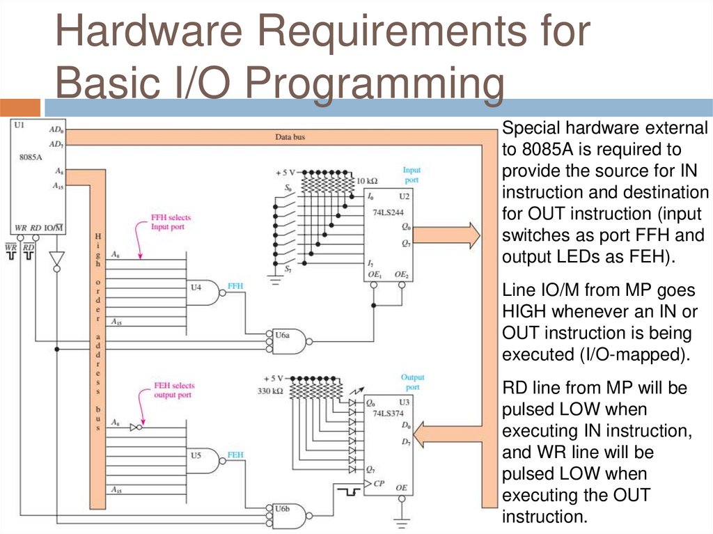
Hardware Requirements forBasic I/O Programming
◻
This was an example of memory-mapped I/O
◻ input and output devices were accessed as if they
were memory locations by specifying their unique
16-bit address
◻
other technique is standard I/O or I/O-mapped
I/O
◻ identify their input and output devices by giving
them an 8-bit port number
◻ The microprocessor then accesses the I/O ports
by using the instructions OUT port and IN port
◻ where port is 00H to FFH
14.
Hardware Requirements forBasic I/O Programming
Special hardware external
to 8085A is required to
provide the source for IN
instruction and destination
for OUT instruction (input
switches as port FFH and
output LEDs as FEH).
Line IO/M from MP goes
HIGH whenever an IN or
OUT instruction is being
executed (I/O-mapped).
RD line from MP will be
pulsed LOW when
executing IN instruction,
and WR line will be
pulsed LOW when
executing the OUT
instruction.
15.
Writing Assembly Languageand Machine Language
Programs
◻
conversion from assembly to machine language involves translating
each mnemonic into appropriate hexadecimal machine code and
storing these codes in specific memory addresses
◻
assembly language is classified as a low-level language because
programmer has to take care of all the most minute details
◻
high-level languages (Pascal, FORTRAN, C, BASIC) are much
easier to write but are not as memory efficient or as fast as
assembly language
but all of them get reduced to machine language code before they can
be executed by microprocessor
◻ conversion from high-level languages to machine code is done by a
compiler
◻
◻
assembly language and its corresponding machine code differ
depending on processor
◻
however fundamentals of the different assembly languages are the
same
16.
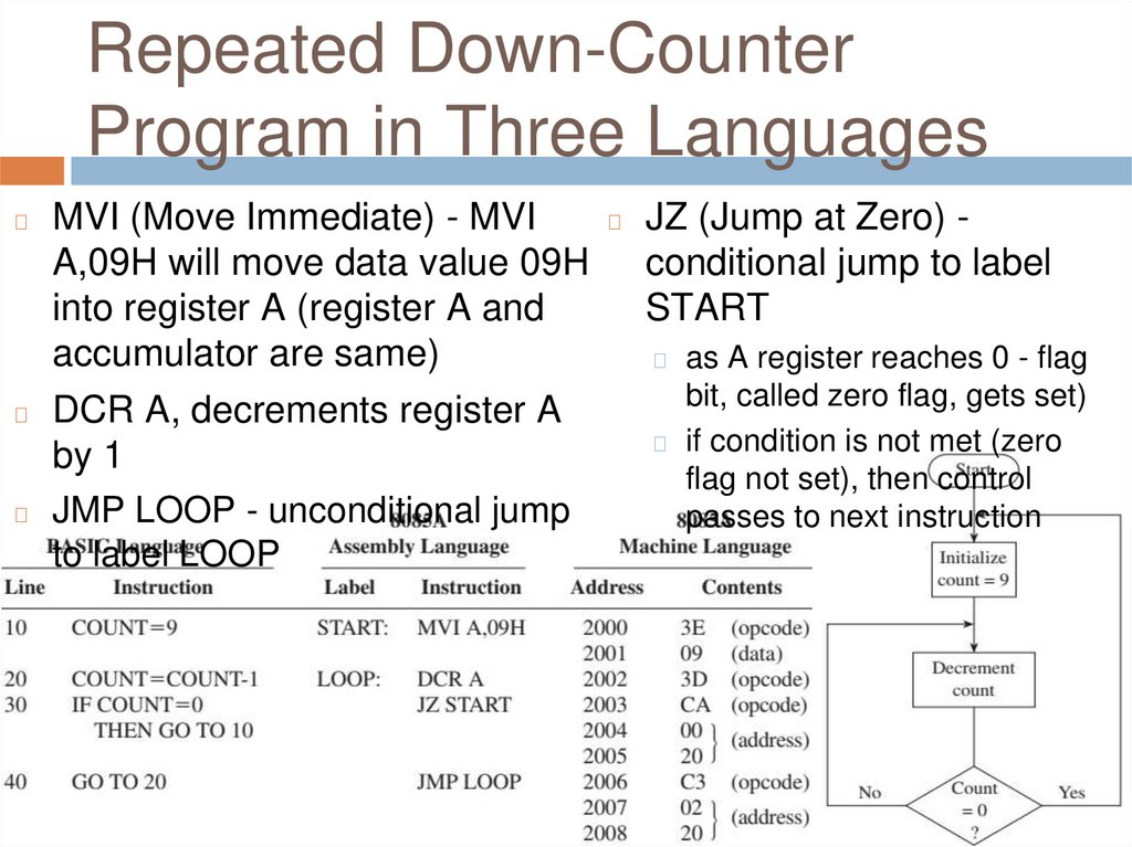
Repeated Down-CounterProgram in Three Languages
MVI (Move Immediate) - MVI
◻ JZ (Jump at Zero) A,09H will move data value 09H conditional jump to label
into register A (register A and
START
accumulator are same)
◻ as A register reaches 0 - flag
bit, called zero flag, gets set)
◻ DCR A, decrements register A
◻ if condition is not met (zero
by 1
flag not set), then control
◻ JMP LOOP - unconditional jump
passes to next instruction
to label LOOP
◻
17.
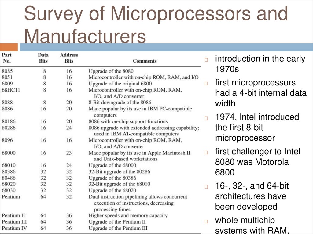
Survey of Microprocessors andManufacturers
◻
introduction in the early
1970s
◻
first microprocessors
had a 4-bit internal data
width
◻
1974, Intel introduced
the first 8-bit
microprocessor
◻
first challenger to Intel
8080 was Motorola
6800
◻
16-, 32-, and 64-bit
architectures have
been developed
◻
whole multichip
systems with RAM,
18.
Review Questions1.
2.
3.
4.
Why is the instruction LDA 4000H called a 3-byte
instruction?
When executing the instruction LDA 4000H, the
microprocessor fetches the machine code from
RAM location 4000H. True or false?
Programs written in assembly language must be
converted to machine code before being
executed by a microprocessor. True or false?
Programs written in a high-level language are
more memory efficient than those written in
assembly language. True or false?
19.
The 8051 Microcontrollermicrocontroller has the CPU, RAM, ROM, timer/counter,
and parallel and serial I/O ports fabricated into a single
IC
◻ CPU’s instruction set is improved for control applications
and offers bit-oriented data manipulation, branching, and
I/O, as well as multiply and divide instructions
◻ most efficiently used in systems that have a fixed
program for a dedicated application (keyboard, car,
ATM, etc…)
◻ for internal memory it has a 4Kx8 ROM and a 128x8
RAM
◻ It has two 16-bit counter/timers and interrupt control for
five interrupt sources
◻
20.
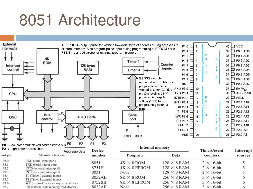
8051 ArchitectureALE/PROG - output pulse for latching low-order byte of address during accesses to
external memory. Also program pulse input during programming of EPROM parts
PSEN - is a read strobe for external program memory
EA/VPP - enable
microcontroller to fetch its
program code from an
external memory IC. This
pin also receives 21-V
programming supply
voltage (VPP) for
programming EPROM
parts
P0 -> low-order multiplexed address/data bus
P2 -> high-order address bus
21.
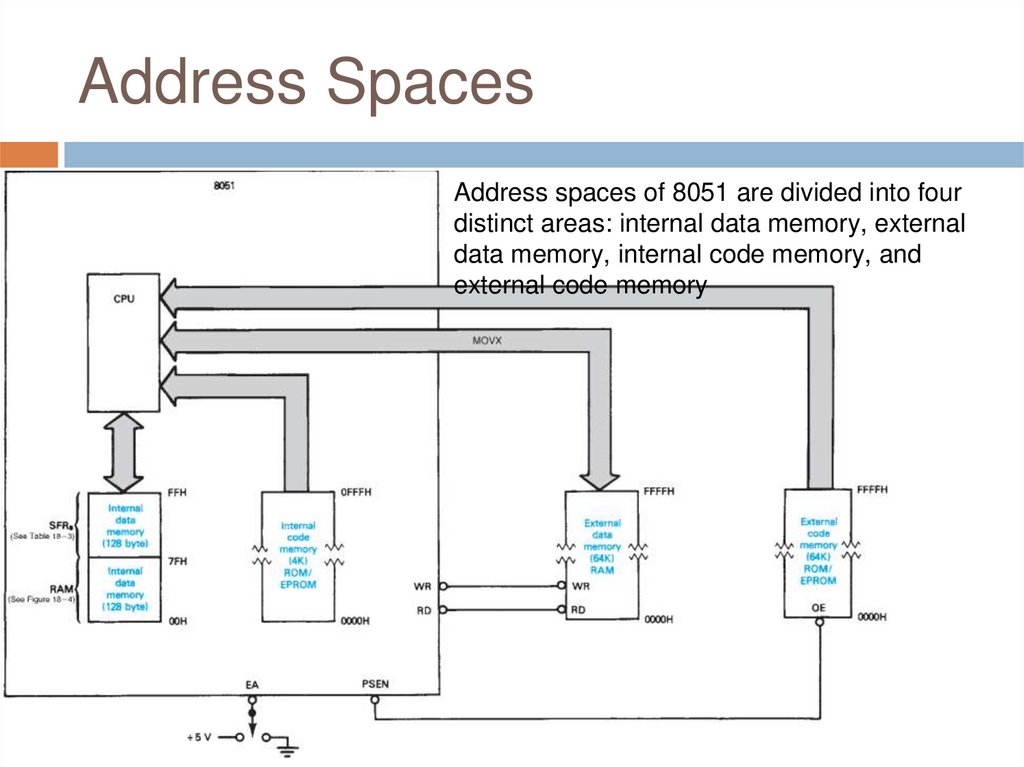
Address SpacesAddress spaces of 8051 are divided into four
distinct areas: internal data memory, external
data memory, internal code memory, and
external code memory
22.
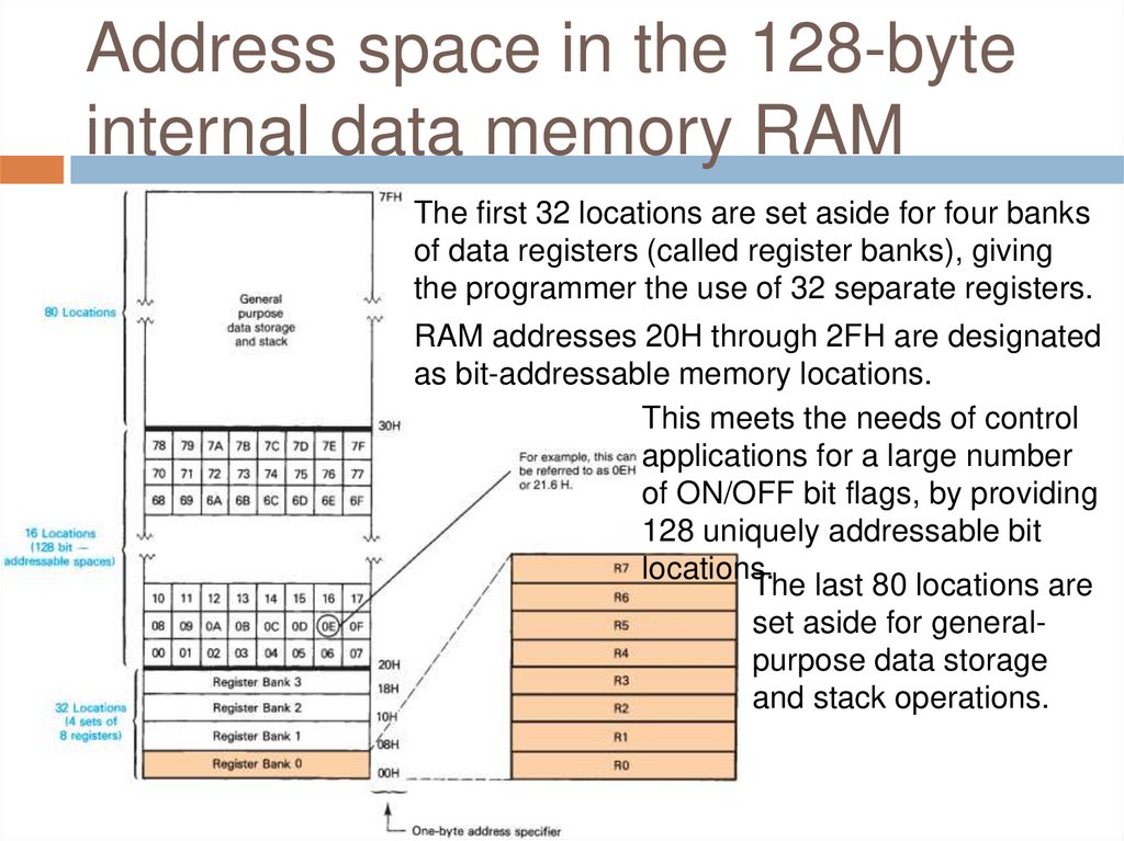
Address space in the 128-byteinternal data memory RAM
The first 32 locations are set aside for four banks
of data registers (called register banks), giving
the programmer the use of 32 separate registers.
RAM addresses 20H through 2FH are designated
as bit-addressable memory locations.
This meets the needs of control
applications for a large number
of ON/OFF bit flags, by providing
128 uniquely addressable bit
locations.
The last 80 locations are
set aside for generalpurpose data storage
and stack operations.
23.
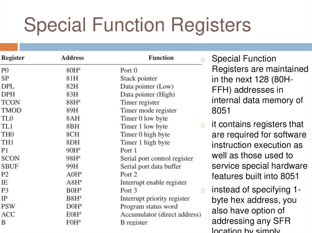
Special Function Registers◻
Special Function
Registers are maintained
in the next 128 (80HFFH) addresses in
internal data memory of
8051
◻
it contains registers that
are required for software
instruction execution as
well as those used to
service special hardware
features built into 8051
◻
instead of specifying 1byte hex address, you
also have option of
addressing any SFR
24.
Q&AAny Questions?