Similar presentations:
CPU How It Works
1. CPU How It Works
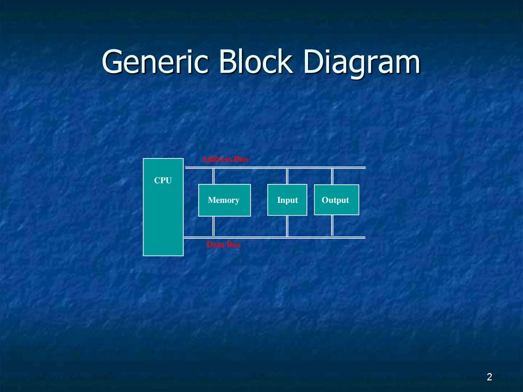
2. Generic Block Diagram
Address BusCPU
Memory
Input
Output
Data Bus
2
3. Hardware
4. The Von Neumann Architecture
Von NeumannArchitecture
5. Designing Computers
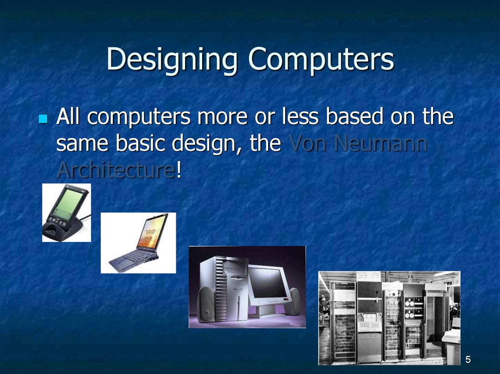
All computers more or less based on thesame basic design, the Von Neumann
Architecture!
5
6. The Von Neumann Architecture
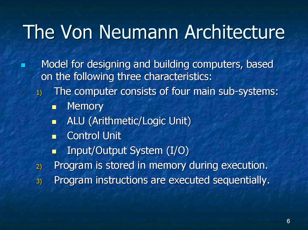
Model for designing and building computers, basedon the following three characteristics:
1)
The computer consists of four main sub-systems:
Memory
ALU (Arithmetic/Logic Unit)
Control Unit
Input/Output System (I/O)
2)
Program is stored in memory during execution.
3)
Program instructions are executed sequentially.
6
7. The Von Neumann Architecture
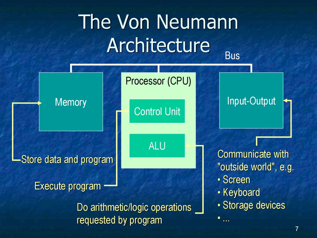
BusProcessor (CPU)
Memory
Control Unit
ALU
Store data and program
Execute program
Do arithmetic/logic operations
requested by program
Input-Output
Communicate with
"outside world", e.g.
• Screen
• Keyboard
• Storage devices
• ...
7
8. Memory Subsystem
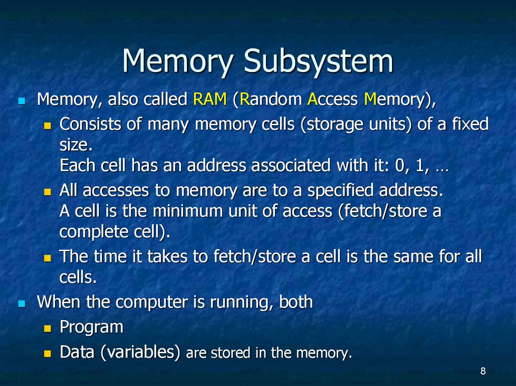
Memory, also called RAM (Random Access Memory),Consists of many memory cells (storage units) of a fixed
size.
Each cell has an address associated with it: 0, 1, …
All accesses to memory are to a specified address.
A cell is the minimum unit of access (fetch/store a
complete cell).
The time it takes to fetch/store a cell is the same for all
cells.
When the computer is running, both
Program
Data (variables) are stored in the memory.
8
9. Memory Size / Speed
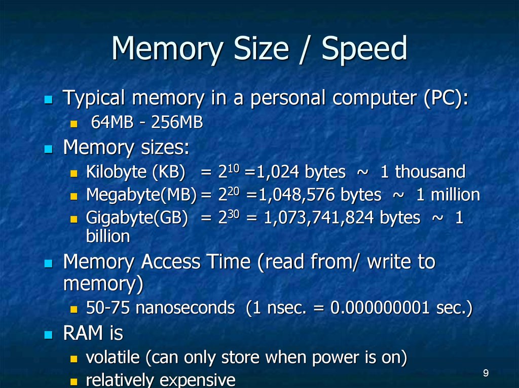
Typical memory in a personal computer (PC):Memory sizes:
Kilobyte (KB) = 210 =1,024 bytes ~ 1 thousand
Megabyte(MB) = 220 =1,048,576 bytes ~ 1 million
Gigabyte(GB) = 230 = 1,073,741,824 bytes ~ 1
billion
Memory Access Time (read from/ write to
memory)
64MB - 256MB
50-75 nanoseconds (1 nsec. = 0.000000001 sec.)
RAM is
volatile (can only store when power is on)
relatively expensive
9
10. Operations on Memory
Fetch (address):Store (address, value):
Fetch a copy of the content of memory cell with the
specified address.
Non-destructive, copies value in memory cell.
Store the specified value into the memory cell specified
by address.
Destructive, overwrites the previous value of the
memory cell.
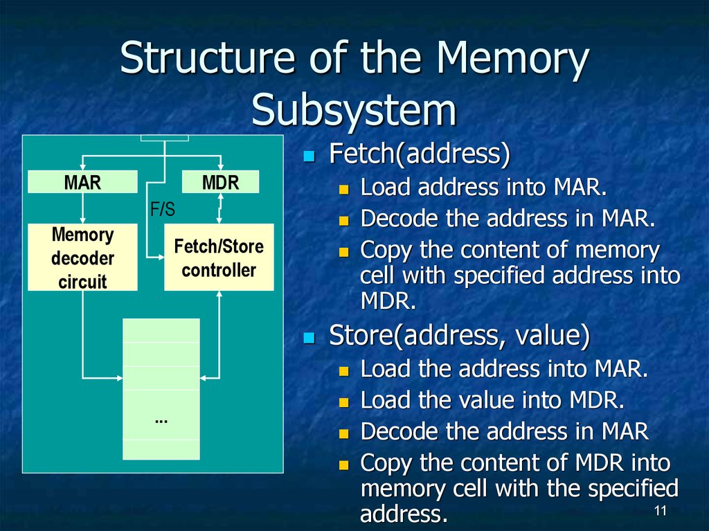
The memory system is interfaced via:
Memory Address Register (MAR)
Memory Data Register (MDR)
Fetch/Store signal
10
11. Structure of the Memory Subsystem
MARMDR
F/S
Memory
decoder
circuit
Fetch(address)
Fetch/Store
controller
Store(address, value)
...
Load address into MAR.
Decode the address in MAR.
Copy the content of memory
cell with specified address into
MDR.
Load the address into MAR.
Load the value into MDR.
Decode the address in MAR
Copy the content of MDR into
memory cell with the specified
11
address.
12. Input/Output Subsystem
Handles devices that allow the computer system to:Communicate and interact with the outside world
Screen, keyboard, printer, ...
Store information (mass-storage)
Hard-drives, floppies, CD, tapes, …
Mass-Storage Device Access Methods:
Direct Access Storage Devices (DASDs)
Hard-drives, floppy-disks, CD-ROMs, ...
Sequential Access Storage Devices (SASDs)
Tapes (for example, used as backup devices)
12
13. I/O Controllers
Speed of I/O devices is slow compared to RAMRAM ~ 50 nsec.
Hard-Drive ~ 10msec. = (10,000,000 nsec)
Solution:
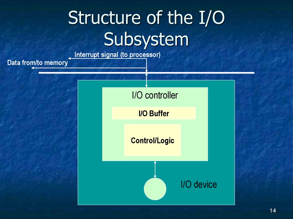
I/O Controller, a special purpose processor:
Has a small memory buffer, and a control logic to
control I/O device (e.g. move disk arm).
Sends an interrupt signal to CPU when done
read/write.
Data transferred between RAM and memory buffer.
Processor free to do something else while I/O
controller reads/writes data from/to device into I/O
buffer.
13
14. Structure of the I/O Subsystem
Data from/to memoryInterrupt signal (to processor)
I/O controller
I/O Buffer
Control/Logic
I/O device
14
15. The ALU Subsystem
The ALU (Arithmetic/Logic Unit) performsmathematical operations (+, -, x, /, …)
logic operations (=, <, >, and, or, not, ...)
In today's computers integrated into the
CPU
Consists of:
Circuits to do the arithmetic/logic operations.
Registers (fast storage units) to store
intermediate computational results.
Bus that connects the two.
15
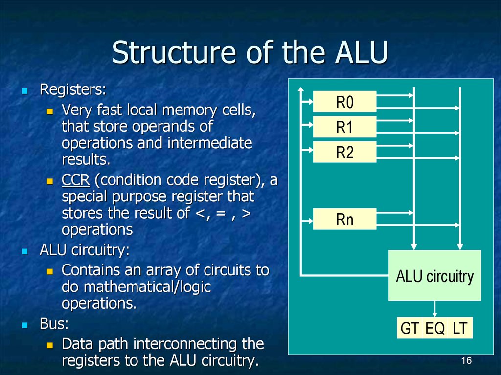
16. Structure of the ALU
Registers:Very fast local memory cells,
that store operands of
operations and intermediate
results.
CCR (condition code register), a
special purpose register that
stores the result of <, = , >
operations
ALU circuitry:
Contains an array of circuits to
do mathematical/logic
operations.
Bus:
Data path interconnecting the
registers to the ALU circuitry.
R0
R1
R2
Rn
ALU circuitry
GT EQ LT
16
17. The Control Unit
Program is stored in memoryas machine language instructions, in binary
The task of the control unit is to execute programs by
repeatedly:
Fetch from memory the next instruction to be
executed.
Decode it, that is, determine what is to be done.
Execute it by issuing the appropriate signals to the
ALU, memory, and I/O subsystems.
Continues until the HALT instruction
17
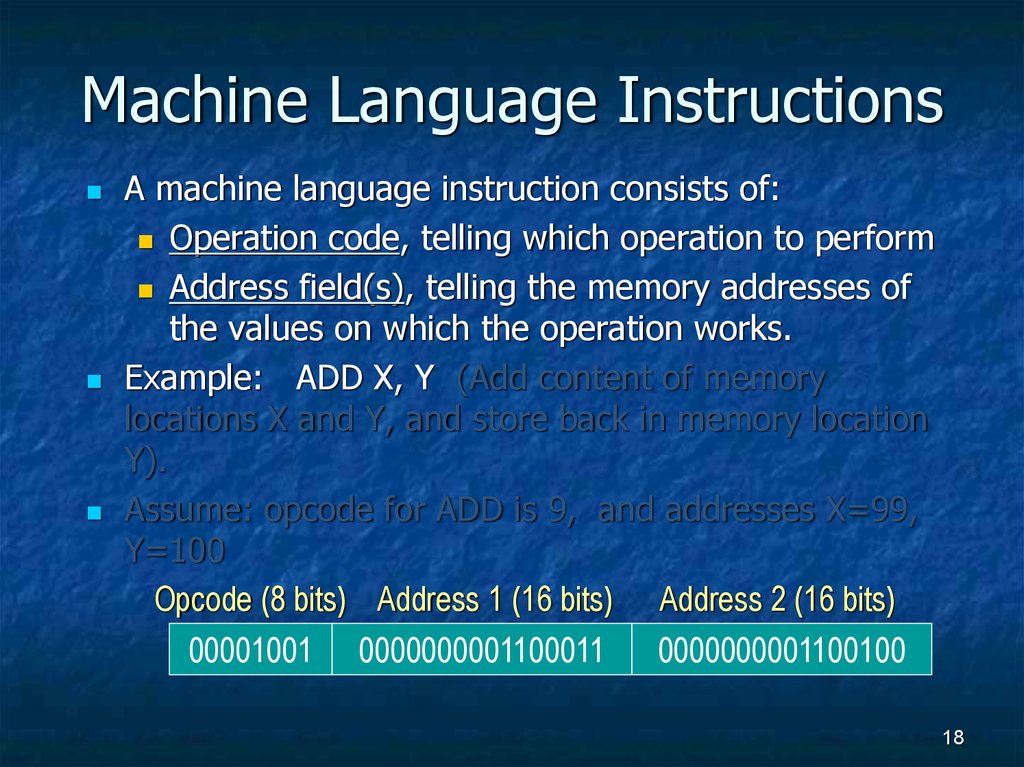
18. Machine Language Instructions
A machine language instruction consists of:Operation code, telling which operation to perform
Address field(s), telling the memory addresses of
the values on which the operation works.
Example: ADD X, Y (Add content of memory
locations X and Y, and store back in memory location
Y).
Assume: opcode for ADD is 9, and addresses X=99,
Y=100
Opcode (8 bits) Address 1 (16 bits) Address 2 (16 bits)
00001001 0000000001100011
0000000001100100
18
19. How does this all work together?
Program Execution:PC is set to the address where the first
program instruction is stored in memory.
Repeat until HALT instruction or fatal error
Fetch instruction
Decode instruction
Execute instruction
End of loop
19
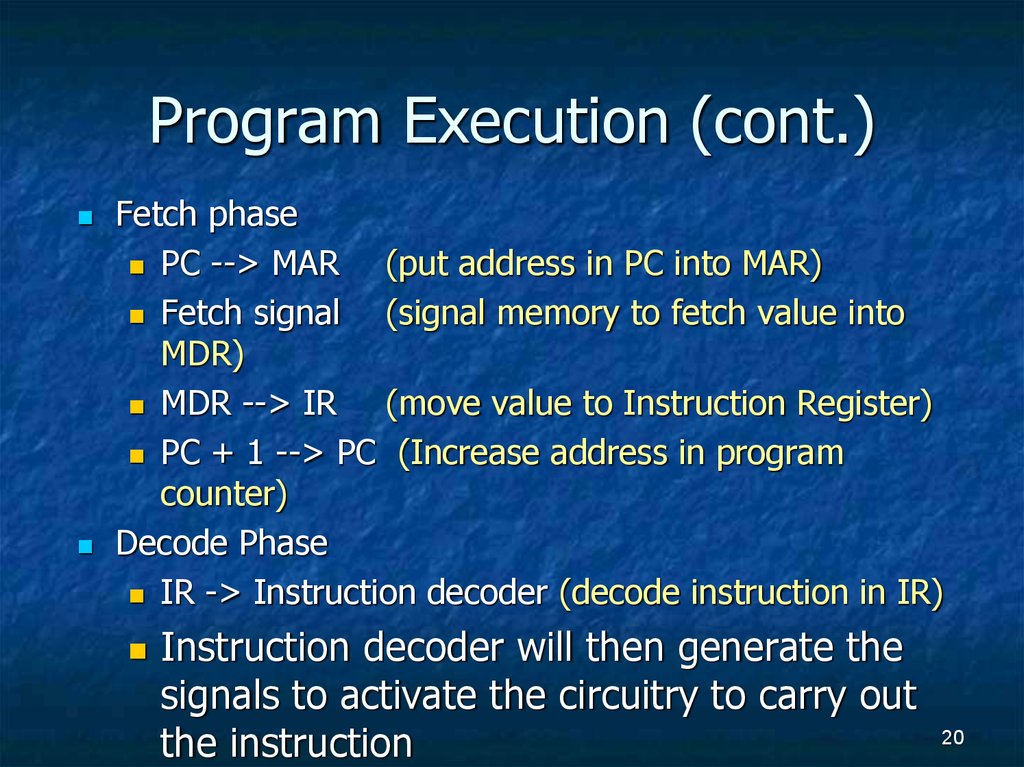
20. Program Execution (cont.)
Fetch phasePC --> MAR
(put address in PC into MAR)
Fetch signal
(signal memory to fetch value into
MDR)
MDR --> IR
(move value to Instruction Register)
PC + 1 --> PC (Increase address in program
counter)
Decode Phase
IR -> Instruction decoder (decode instruction in IR)
Instruction decoder will then generate the
signals to activate the circuitry to carry out
the instruction
20
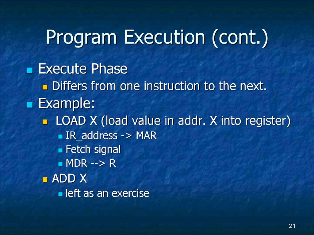
21. Program Execution (cont.)
Execute PhaseDiffers from one instruction to the next.
Example:
LOAD X (load value in addr. X into register)
IR_address -> MAR
Fetch signal
MDR --> R
ADD X
left as an exercise
21



 informatics


