
 electronics
Similar presentations:

")


")

Programmable Logic Devices: CPLDs and FPGAs with VHDL
1.
Programmable Logic Devices:CPLDs and FPGAs with VHDL
Design
Lecture 3
Digital Electronics
2.
Course MaterialsAll needed Software and course materials will
be located on Canvas.
◻ Materials that are used in this slides are taken
from the textbook “Digital Electronics A
Practical Approach with VHDL” by William
Kleitz
◻
3.
Programmable Logic Devices:CPLDs, FPGAs with VHDL
Design
◻
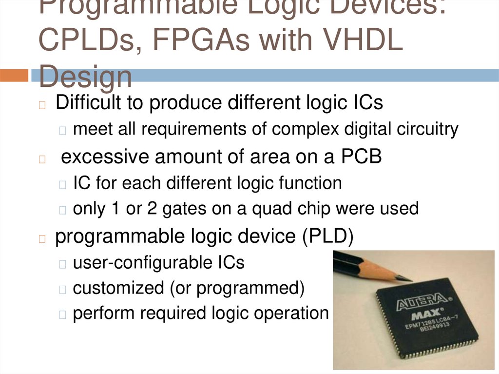
Difficult to produce different logic ICs
◻ meet all requirements of complex digital circuitry
◻
excessive amount of area on a PCB
◻ IC for each different logic function
◻ only 1 or 2 gates on a quad chip were used
◻
programmable logic device (PLD)
◻ user-configurable ICs
◻ customized (or programmed)
◻ perform required logic operation
4.
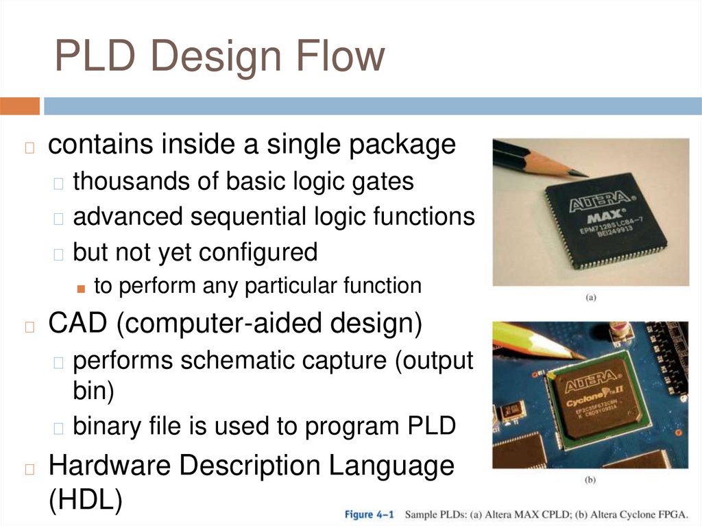
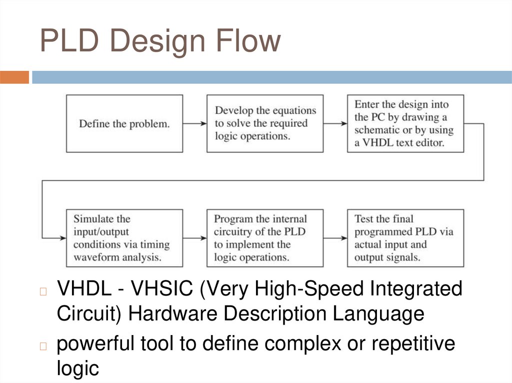
PLD Design Flow◻
contains inside a single package
◻ thousands of basic logic gates
◻ advanced sequential logic functions
◻ but not yet configured
■ to perform any particular function
◻
CAD (computer-aided design)
◻ performs schematic capture (output
bin)
◻ binary file is used to program PLD
◻
Hardware Description Language
(HDL)
5.
PLD Design FlowVHDL - VHSIC (Very High-Speed Integrated
Circuit) Hardware Description Language
◻ powerful tool to define complex or repetitive
logic
◻
6.
Power of a PLDVS
7.
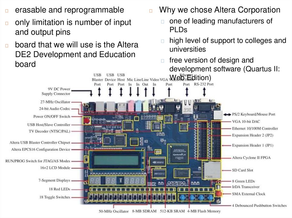
◻erasable and reprogrammable
◻
only limitation is number of input
and output pins
◻
board that we will use is the Altera
DE2 Development and Education
board
◻
Why we chose Altera Corporation
one of leading manufacturers of
PLDs
◻ high level of support to colleges and
universities
◻ free version of design and
development software (Quartus II:
Web Edition)
◻
8.
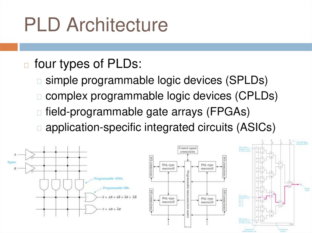
PLD Architecture◻
four types of PLDs:
◻ simple programmable logic devices (SPLDs)
◻ complex programmable logic devices (CPLDs)
◻ field-programmable gate arrays (FPGAs)
◻ application-specific integrated circuits (ASICs)
9.
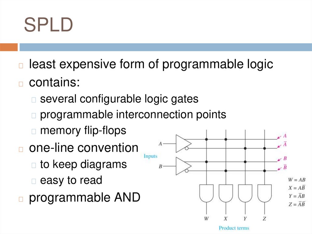
SPLDleast expensive form of programmable logic
◻ contains:
◻
◻ several configurable logic gates
◻ programmable interconnection points
◻ memory flip-flops
◻
one-line convention
◻ to keep diagrams
◻ easy to read
◻
programmable ANDs
10.
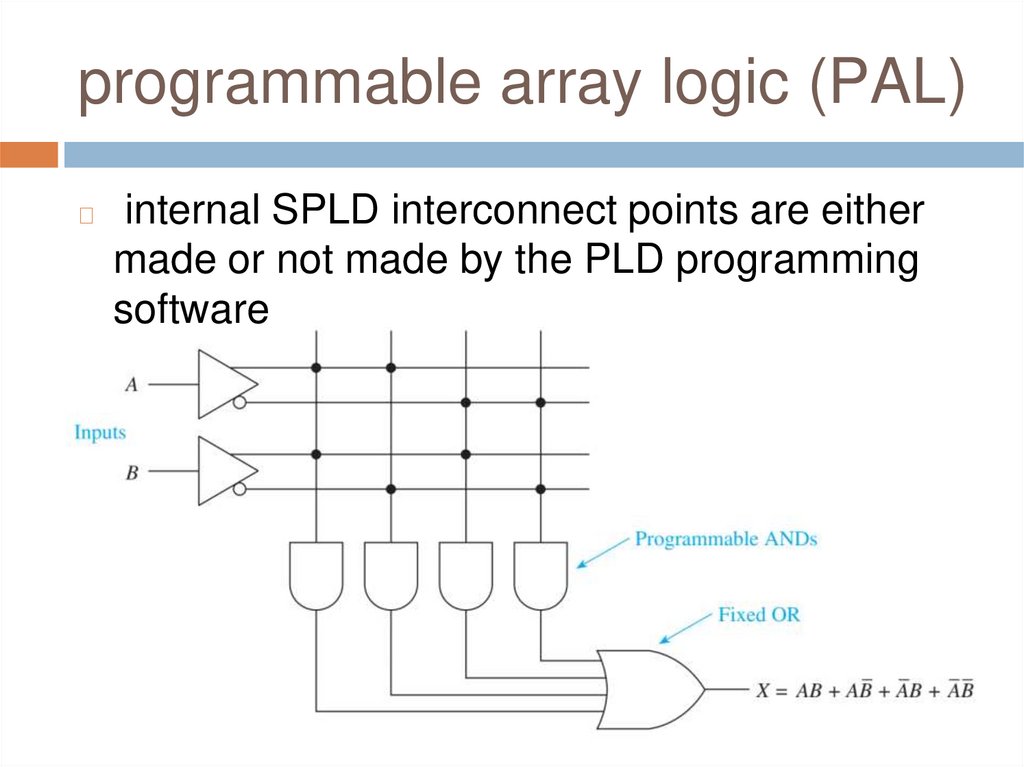
programmable array logic (PAL)◻
internal SPLD interconnect points are either
made or not made by the PLD programming
software
11.
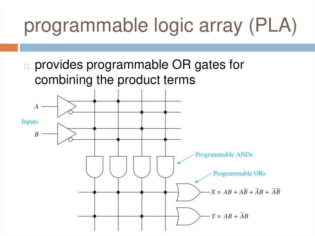
programmable logic array (PLA)◻
provides programmable OR gates for
combining the product terms
12.
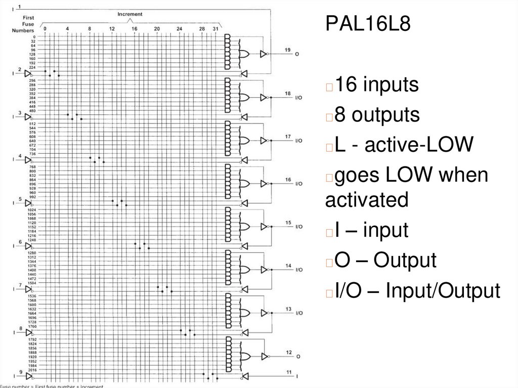
PAL16L816 inputs
◻8 outputs
◻L - active-LOW
◻goes LOW when
activated
◻I – input
◻O – Output
◻I/O – Input/Output
◻
13.
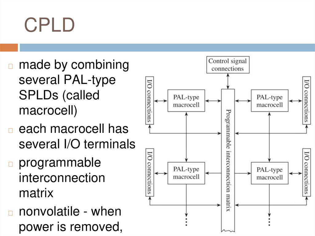
CPLDmade by combining
several PAL-type
SPLDs (called
macrocell)
◻ each macrocell has
several I/O terminals
◻ programmable
interconnection
matrix
◻ nonvolatile - when
power is removed,
◻
14.
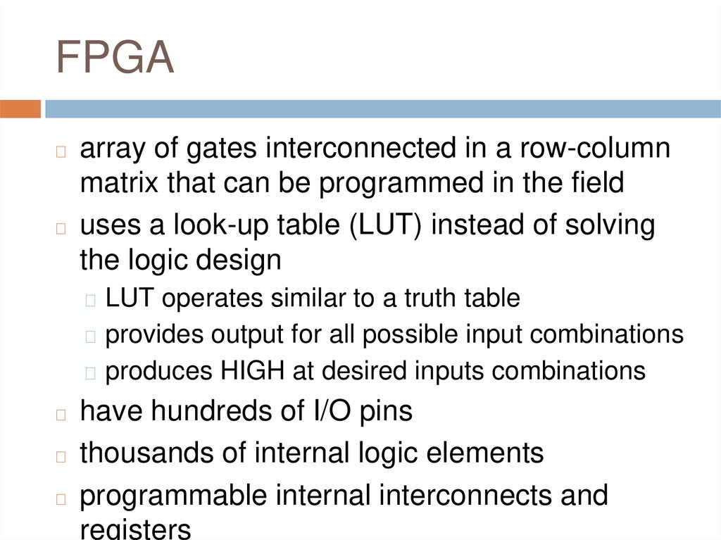
FPGAarray of gates interconnected in a row-column
matrix that can be programmed in the field
◻ uses a look-up table (LUT) instead of solving
the logic design
◻
◻ LUT operates similar to a truth table
◻ provides output for all possible input combinations
◻ produces HIGH at desired inputs combinations
have hundreds of I/O pins
◻ thousands of internal logic elements
◻ programmable internal interconnects and
registers
◻
15.
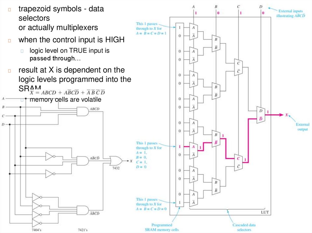
◻trapezoid symbols - data
selectors
or actually multiplexers
◻
when the control input is HIGH
◻
◻
logic level on TRUE input is
passed through…
result at X is dependent on the
logic levels programmed into the
SRAM
◻
memory cells are volatile
16.
application-specific integratedcircuit (ASIC)
◻
design that has been created and tested on an
FPGA can be transferred to an ASIC
◻ if there is a large quantity demand
the logic function is hard-coded into the IC
◻ non-volatile - user does not have to
reconfigure the IC at each power-on
◻ Altera DE-2 Development board contains
FPGA
◻
◻ Cyclone EP2C35F672C6N
◻ 33 216 look-up tables
◻ 475 pins dedicated for input/output
17.
Review Questions1.
2.
3.
4.
FPGA uses __________ instead of solving
the logic design?
HDL stands for _____________________?
__________ (PLA / PAL) provides
programmable OR gates for combining the
product terms?
Memory cells in FPGA are volatile. True /
False ?
18.
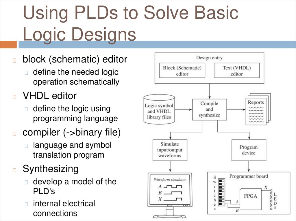
Using PLDs to Solve BasicLogic Designs
◻
block (schematic) editor
◻
◻
VHDL editor
◻
◻
define the logic using
programming language
compiler (->binary file)
◻
◻
define the needed logic
operation schematically
language and symbol
translation program
Synthesizing
develop a model of the
PLD’s
◻ internal electrical
connections
◻
19.
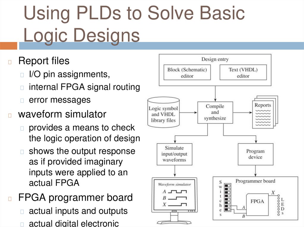
Using PLDs to Solve BasicLogic Designs
◻
Report files
◻ I/O pin assignments,
◻ internal FPGA signal routing
◻ error messages
◻
waveform simulator
◻ provides a means to check
the logic operation of design
◻ shows the output response
as if provided imaginary
inputs were applied to an
actual FPGA
◻
FPGA programmer board
◻ actual inputs and outputs
◻ actual digital electronic
20.
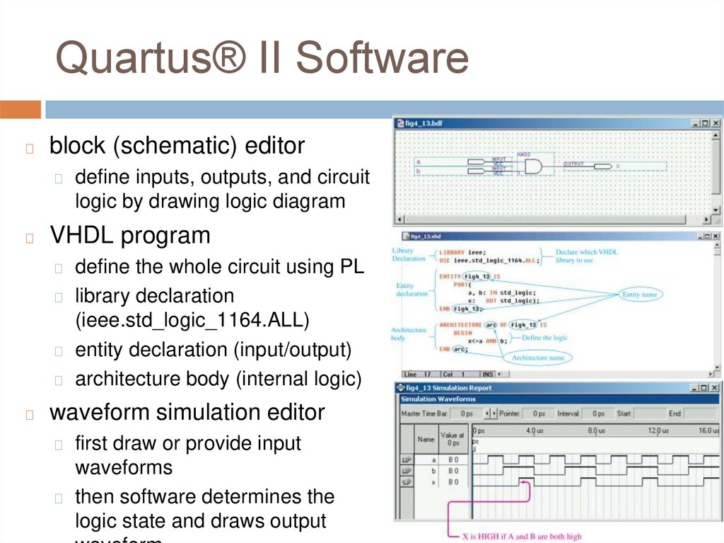
Quartus® II Software◻
block (schematic) editor
◻
◻
define inputs, outputs, and circuit
logic by drawing logic diagram
VHDL program
define the whole circuit using PL
◻ library declaration
(ieee.std_logic_1164.ALL)
◻ entity declaration (input/output)
◻ architecture body (internal logic)
◻
◻
waveform simulation editor
first draw or provide input
waveforms
◻ then software determines the
logic state and draws output
◻
21.
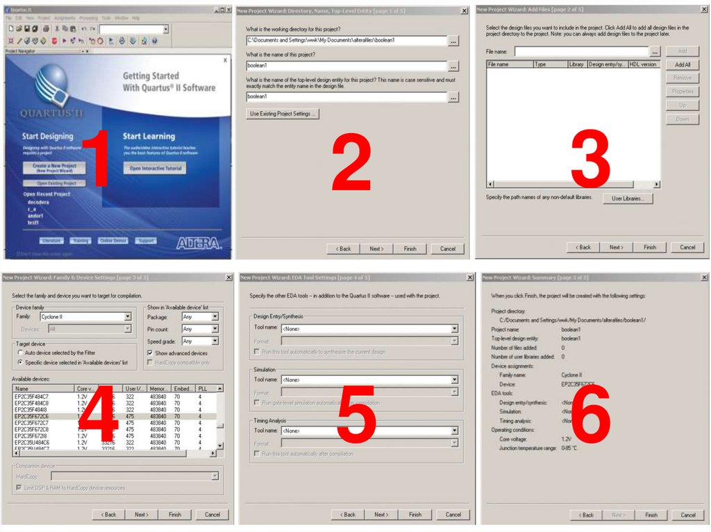
Using Altera’s Quartus® IIDesign and Simulation Software
◻
Download and install
◻ Quartus® II Web Edition version 9.1 sp2
◻ Link to the software is available on Canvas
Start the Altera Quartus® II software
◻ Create a New Project
◻
◻ File -> New Project Wizard
◻ Choose working directory and name for project
◻ Specify FPGA
■ Family - select Cyclone II
■ Specific device - Highlight the EP2C35F672C6
22.
12
3
4
5
6
23.
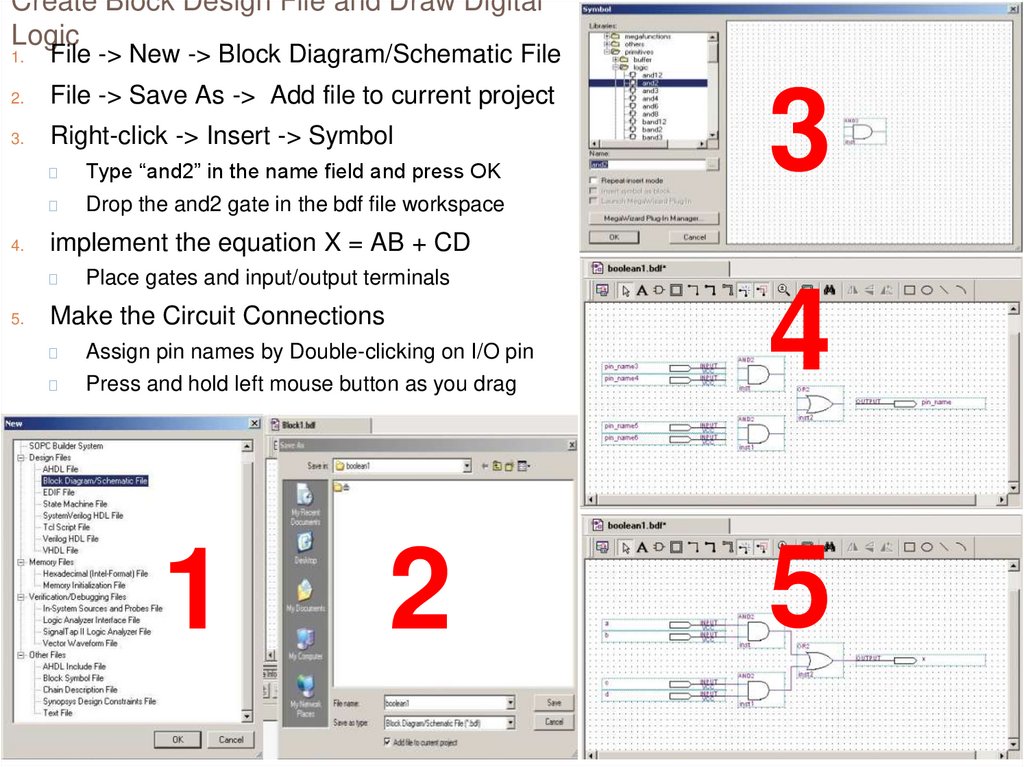
Create Block Design File and Draw DigitalLogic
1.
File -> New -> Block Diagram/Schematic File
2.
File -> Save As -> Add file to current project
3.
Right-click -> Insert -> Symbol
4.
◻
Type “and2” in the name field and press OK
◻
Drop the and2 gate in the bdf file workspace
implement the equation X = AB + CD
◻
5.
3
Place gates and input/output terminals
Make the Circuit Connections
◻
Assign pin names by Double-clicking on I/O pin
◻
Press and hold left mouse button as you drag
1
2
4
5
24.
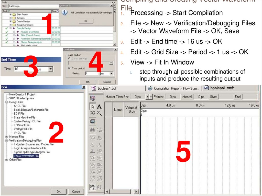
Compiling and Creating Vector WaveformFile
1
4
3
2
1.
Processing -> Start Compilation
2.
File -> New -> Verification/Debugging Files
-> Vector Waveform File -> OK, Save
3.
Edit -> End time -> 16 us -> OK
4.
Edit -> Grid Size -> Period -> 1 us -> OK
5.
View -> Fit In Window
◻
step through all possible combinations of
inputs and produce the resulting output
5
25.
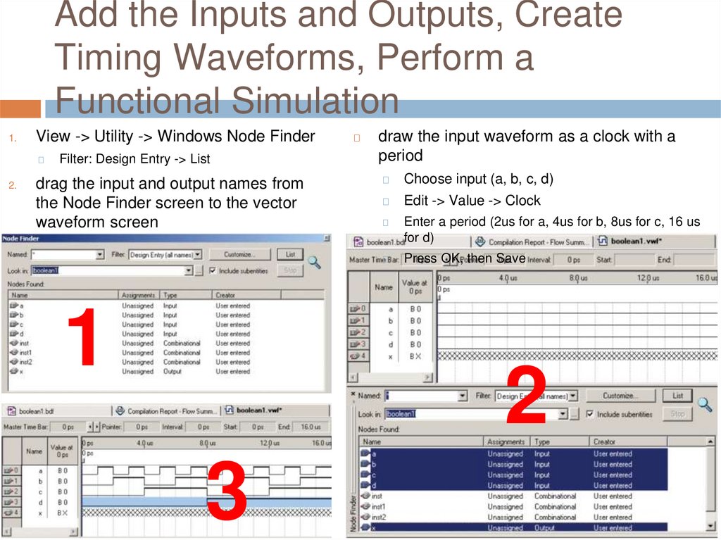
Add the Inputs and Outputs, CreateTiming Waveforms, Perform a
Functional Simulation
1.
View -> Utility -> Windows Node Finder
◻
2.
Filter: Design Entry -> List
drag the input and output names from
the Node Finder screen to the vector
waveform screen
1
◻
draw the input waveform as a clock with a
period
◻
Choose input (a, b, c, d)
◻
Edit -> Value -> Clock
◻
Enter a period (2us for a, 4us for b, 8us for c, 16 us
for d)
◻
Press OK, then Save
2
3
26.
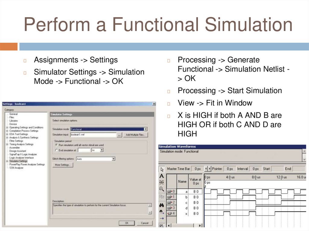
Perform a Functional Simulation◻
Assignments -> Settings
◻
Simulator Settings -> Simulation
Mode -> Functional -> OK
◻
Processing -> Generate
Functional -> Simulation Netlist > OK
◻
Processing -> Start Simulation
◻
View -> Fit in Window
◻
X is HIGH if both A AND B are
HIGH OR if both C AND D are
HIGH
27.
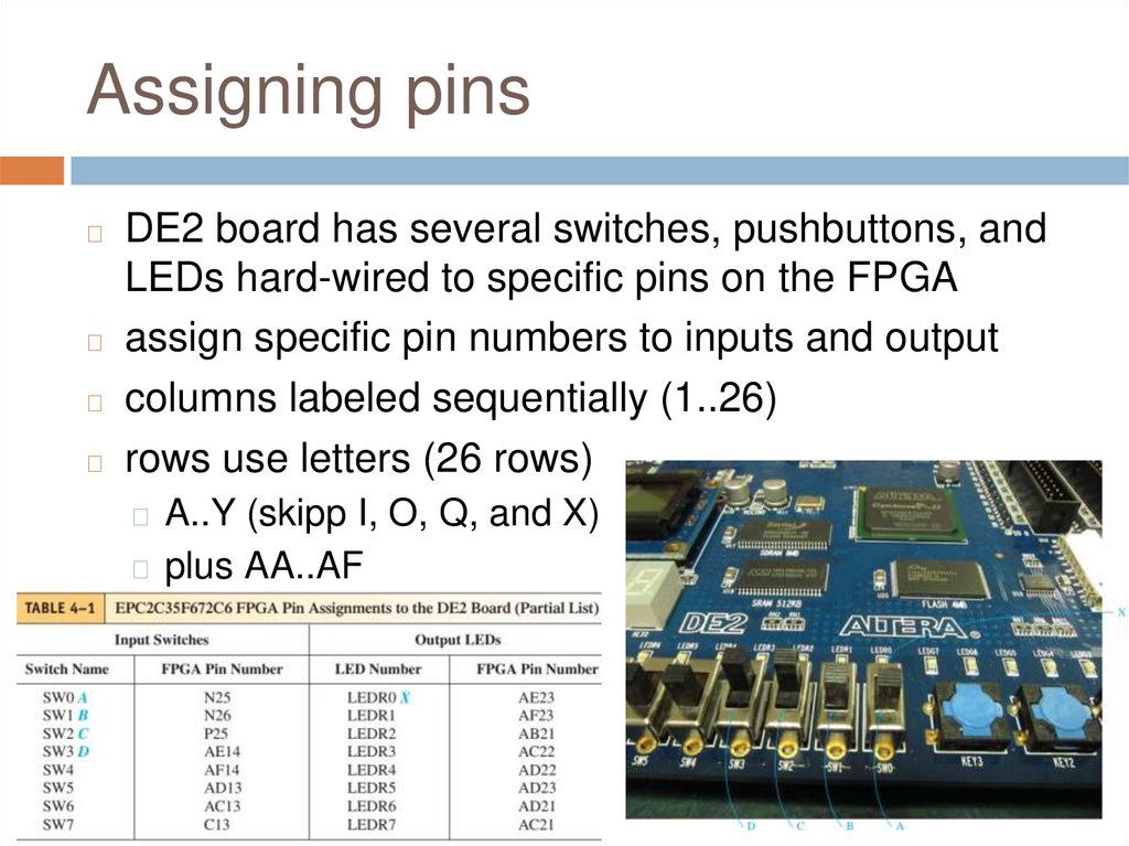
Assigning pinsDE2 board has several switches, pushbuttons, and
LEDs hard-wired to specific pins on the FPGA
◻ assign specific pin numbers to inputs and output
◻ columns labeled sequentially (1..26)
◻ rows use letters (26 rows)
◻
◻ A..Y (skipp I, O, Q, and X)
◻ plus AA..AF
28.
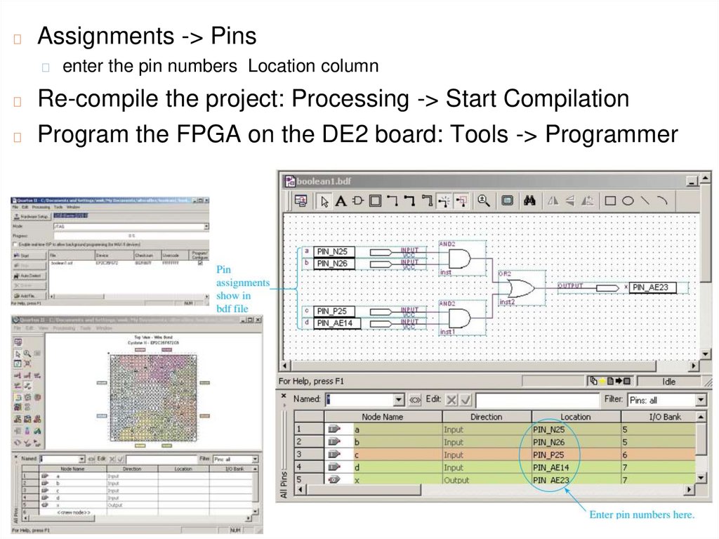
◻Assignments -> Pins
◻
enter the pin numbers Location column
Re-compile the project: Processing -> Start Compilation
◻ Program the FPGA on the DE2 board: Tools -> Programmer
◻
29.
Review Questions1.
2.
3.
___________ (block editor, VHDL program)
defines the needed logic operation
schematically?
Waveform simulator provides a means to
check the logic operation of design. True /
Flase ?
FPGA pin names contain letters which
indicates ________ (row / column) and
numbers which indicate __________ (row /
column) ?
30.
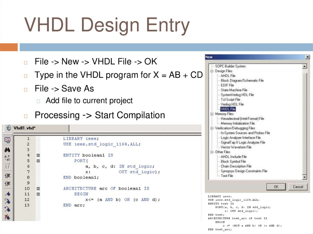
VHDL Design Entry◻
File -> New -> VHDL File -> OK
◻
Type in the VHDL program for X = AB + CD
◻
File -> Save As
◻
◻
Add file to current project
Processing -> Start Compilation
LIBRARY ieee;
USE ieee.std_logic_1164.ALL;
ENTITY test IS
PORT(a, b, c, d: IN std_logic;
x: OUT std_logic);
END test;
ARCHITECTURE test_arc of test IS
BEGIN
x <= (NOT a AND b) OR (c AND d);
END test_arc;
31.
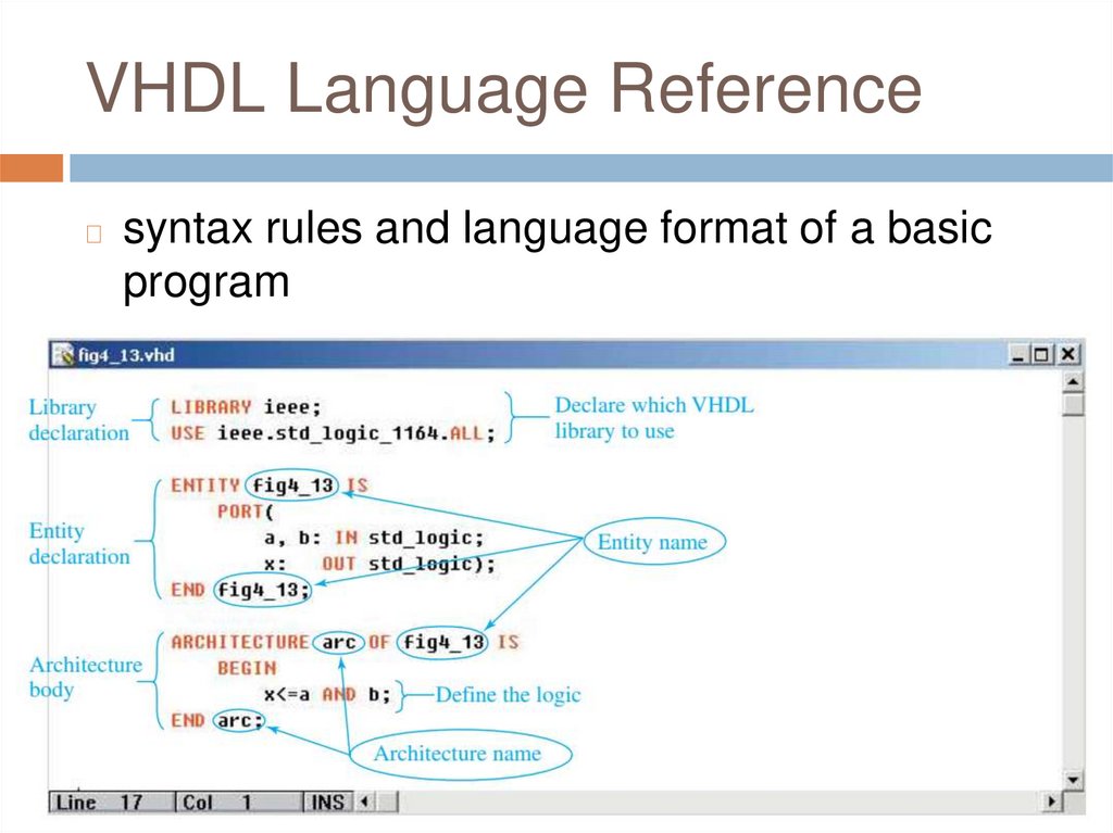
VHDL Language Reference◻
syntax rules and language format of a basic
program
32.
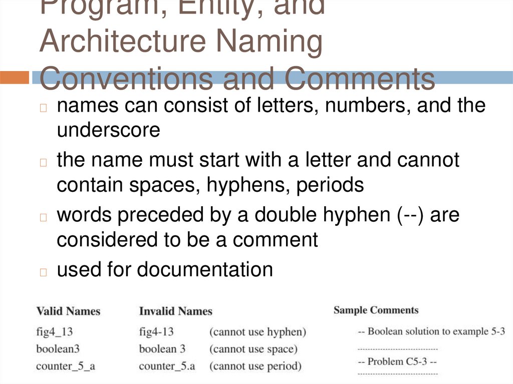
Program, Entity, andArchitecture Naming
Conventions and Comments
names can consist of letters, numbers, and the
underscore
◻ the name must start with a letter and cannot
contain spaces, hyphens, periods
◻ words preceded by a double hyphen (--) are
considered to be a comment
◻ used for documentation
◻
33.
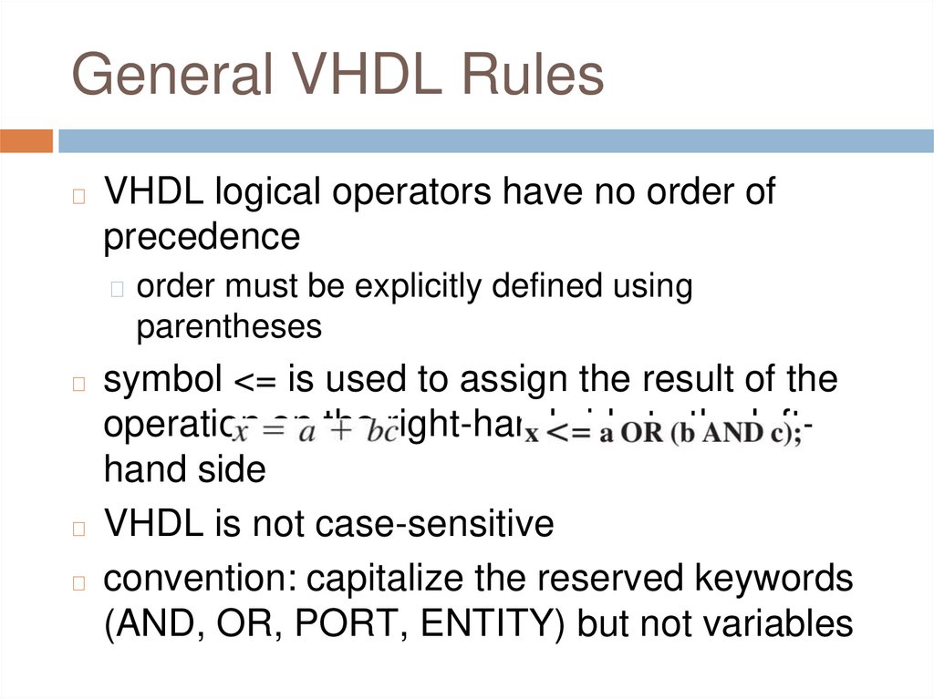
General VHDL Rules◻
VHDL logical operators have no order of
precedence
◻ order must be explicitly defined using
parentheses
symbol <= is used to assign the result of the
operation on the right-hand side to the lefthand side
◻ VHDL is not case-sensitive
◻ convention: capitalize the reserved keywords
(AND, OR, PORT, ENTITY) but not variables
◻
34.
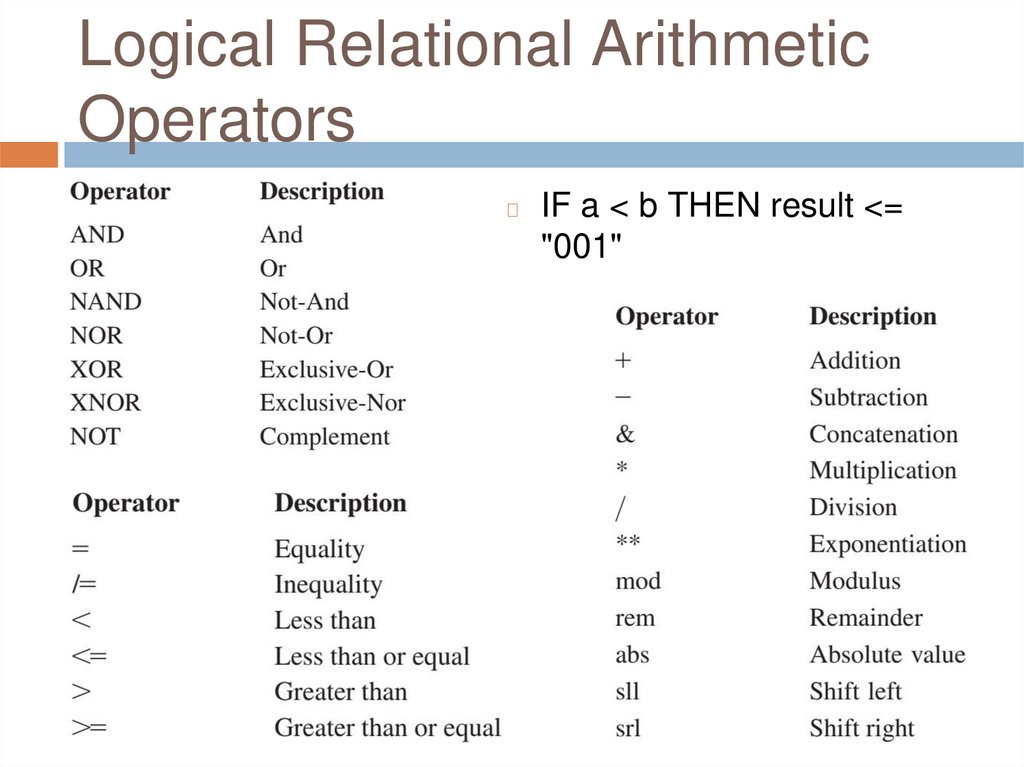
Logical Relational ArithmeticOperators
◻
IF a < b THEN result <=
"001"
35.
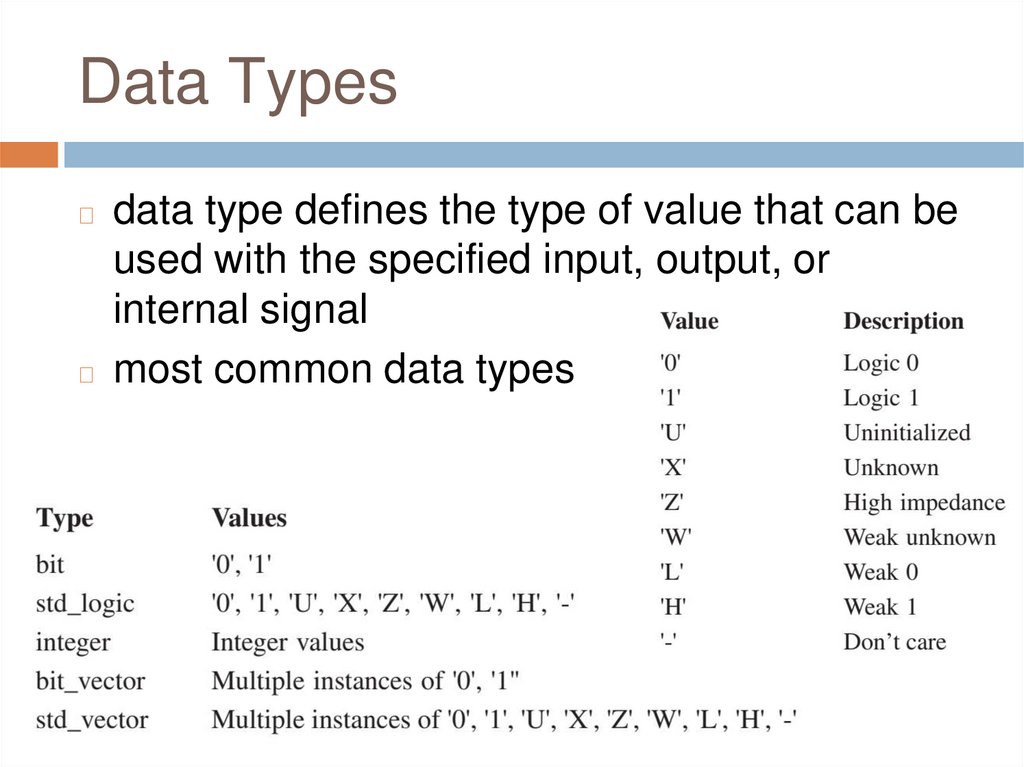
Data Typesdata type defines the type of value that can be
used with the specified input, output, or
internal signal
◻ most common data types
◻
36.
ENTITY & ARCHITECTUREBLOCKS
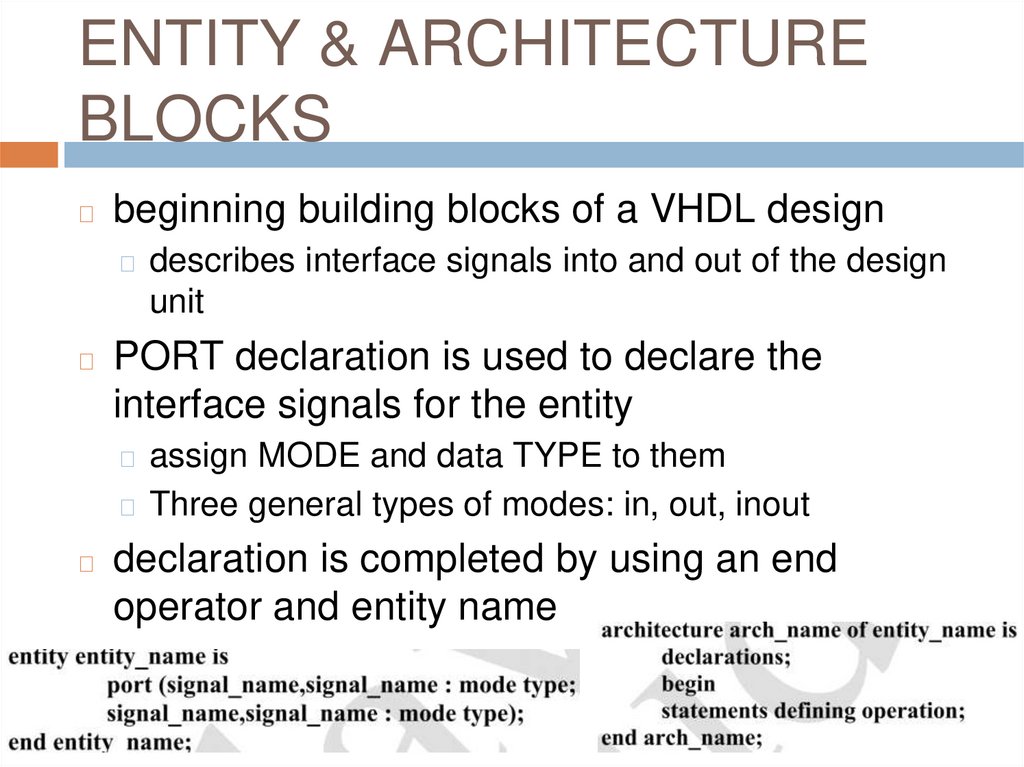
◻
beginning building blocks of a VHDL design
◻ describes interface signals into and out of the design
unit
◻
PORT declaration is used to declare the
interface signals for the entity
◻ assign MODE and data TYPE to them
◻ Three general types of modes: in, out, inout
◻
declaration is completed by using an end
operator and entity name
37.
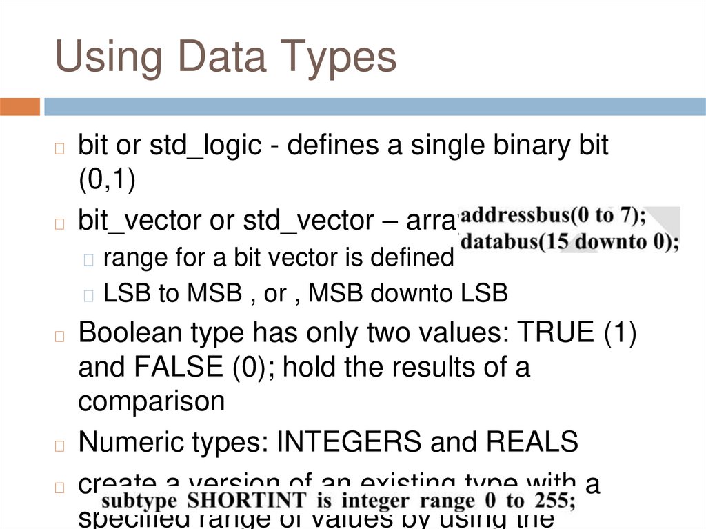
Using Data Typesbit or std_logic - defines a single binary bit
(0,1)
◻ bit_vector or std_vector – array of bits
◻
◻ range for a bit vector is defined
◻ LSB to MSB , or , MSB downto LSB
Boolean type has only two values: TRUE (1)
and FALSE (0); hold the results of a
comparison
◻ Numeric types: INTEGERS and REALS
◻ create a version of an existing type with a
specified range of values by using the
◻
38.
Other Data Types◻
TYPE operator used for creating and defining
user types. Syntax: TYPE type_name (type
values);
◻ TYPE MONTHS (JAN, FEB, MAR, APR, MAY,
JUN, JUL, AUG, SEP, OCT, NOV, DEC);
◻
additional data types
◻ access - acts like a pointer type
◻ file - is used to access a file
◻ physical - finite quantities such as time, voltage…
◻ line - ASCII string of characters
◻ record - contains a collection of multiple data
39.
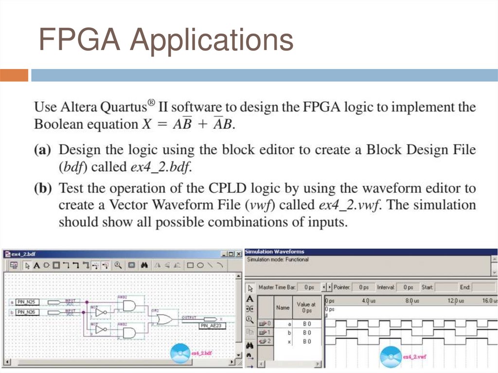
FPGA Applications40.
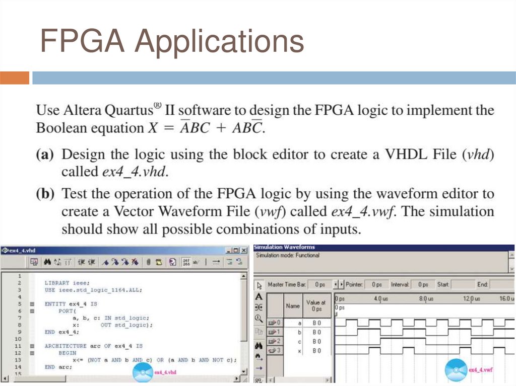
FPGA Applications41.
Review Questions1.
2.
3.
4.
How comments are done in VHDL?
_________ data type defines only two values
(0,1)?
__________ operator is used to assign the
result of the operation on the right-hand side
to the left-hand side?
___________ (TYPE, SUBTYPE) operator
used for creating and defining user types?
42.
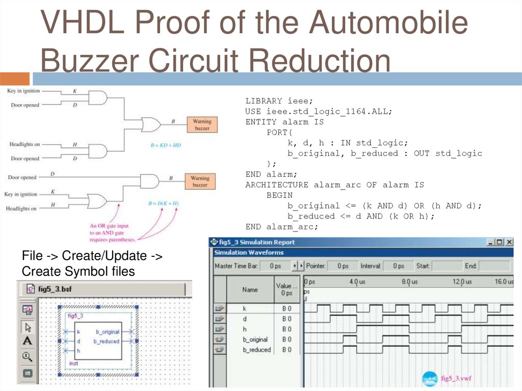
VHDL Proof of the AutomobileBuzzer Circuit Reduction
LIBRARY ieee;
USE ieee.std_logic_1164.ALL;
ENTITY alarm IS
PORT(
k, d, h : IN std_logic;
b_original, b_reduced : OUT std_logic
);
END alarm;
ARCHITECTURE alarm_arc OF alarm IS
BEGIN
b_original <= (k AND d) OR (h AND d);
b_reduced <= d AND (k OR h);
END alarm_arc;
File -> Create/Update ->
Create Symbol files
43.
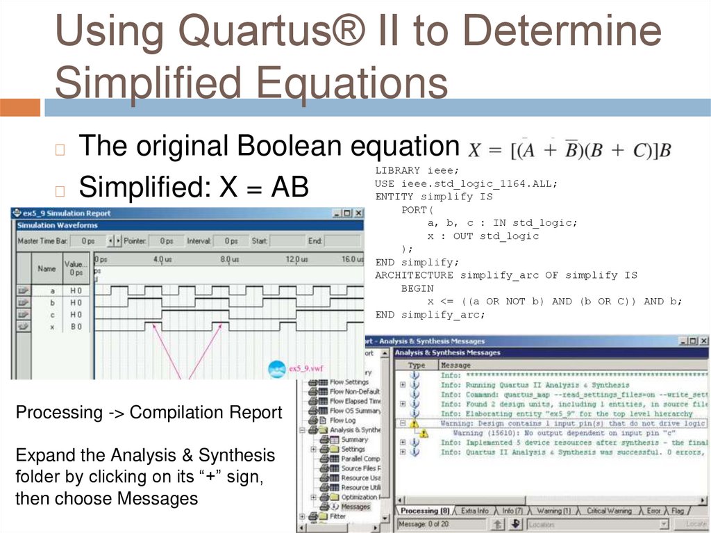
Using Quartus® II to DetermineSimplified Equations
The original Boolean equation
◻ Simplified: X = AB
◻
LIBRARY ieee;
USE ieee.std_logic_1164.ALL;
ENTITY simplify IS
PORT(
a, b, c : IN std_logic;
x : OUT std_logic
);
END simplify;
ARCHITECTURE simplify_arc OF simplify IS
BEGIN
x <= ((a OR NOT b) AND (b OR C)) AND b;
END simplify_arc;
Processing -> Compilation Report
Expand the Analysis & Synthesis
folder by clicking on its “+” sign,
then choose Messages
44.
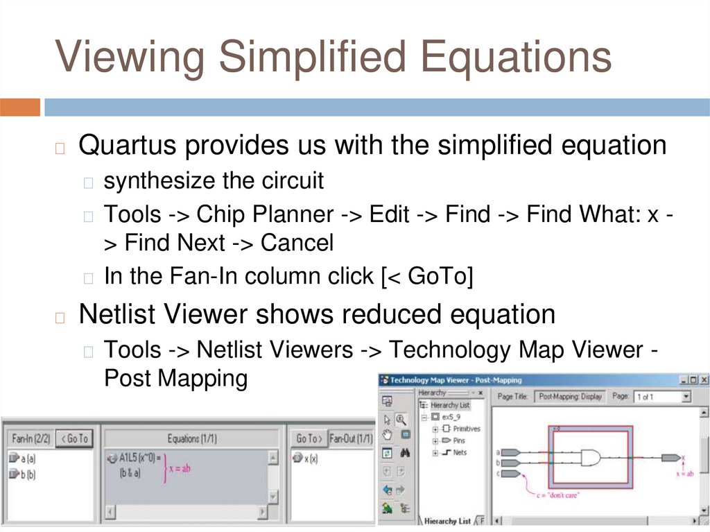
Viewing Simplified Equations◻
Quartus provides us with the simplified equation
◻ synthesize the circuit
◻ Tools -> Chip Planner -> Edit -> Find -> Find What: x -
> Find Next -> Cancel
◻ In the Fan-In column click [< GoTo]
◻
Netlist Viewer shows reduced equation
◻ Tools -> Netlist Viewers -> Technology Map Viewer -
Post Mapping
45.
Q&AAny Questions?