


 Live Demo")
 Live Demo")


")


 – M9703A Target Setup")
 – M9703A Template")
 – M9703A User Design")
 – M9703A User Design")


 Measurement")

 Magnitude")
 Phase")


 Measurement")

")


")
 Programming UI")
 Programming UI")
 Magnitude")
 Phase")


 electronics
Similar presentations:

. Radio management (RM)")


Using systemvue’s open FPGA design flow, M8190A Sig Gen, M9703A High Speed Digitizer
1. Using SystemVue’s Open FPGA Design Flow + M8190A Sig Gen + M9703A High Speed Digitizer
April 17, 20152. Hardware Design Using SystemVue
Signal GenerationSystemVue
3rd Party
HDL Simulators
Graphical Design Entry
System Level Modeling
FPGA Platforms
FPGA
HDL
Files
IP
Textual/Binary Entry
Instrument FPGA
Signal
Analysis
SystemVue, Open
FPGA Design Flow
Page 2
3. SystemVue Hardware Design Kit Model based graphical design tool
Transmit ted {DATAPORT}Data Type= Any Type
Bus= NO
D1 {DelayFxp@Fxp Models}
D2 {DelayFxp@Fxp Models}
D3 {DelayFxp@Fxp Models}
M2 {MpyFxp@Fxp Models}
O ut put PrecisionMode= User Defined
Wordlengt h=16
IntegerWordlength= 2
I sSigned=Signed
M1 {MpyFxp@Fxp Models}
OutputPrecisionMode=User Def ined
Wordlength=16
I ntegerWordlengt h=2
IsSigned= Signed
Received {DATAPORT}
Data Type=Any Type
Bus=NO
A3 {AddFxp@Fxp Models}
Output PrecisionMode=User Def ined
Wordlength=16
IntegerWordlength=2
I sSigned=Signed
M4 {MpyFxp@Fxp Models}
OutputPrecisionMode=User Def ined
Wordlength=16
I ntegerWordlengt h=2
A2 {AddFxp@Fxp Models}
I sSigned= Signed
OutputPrecisionMode= User Defined
Wordlengt h= 16
IntegerWordlengt h= 2
I sSigned= Signed
M3 {MpyFxp@Fxp Models}
O utput PrecisionMode= User Defined
Wordlengt h=16
I nt egerWordlengt h= 2
A1 {AddFxp@Fxp Models}
I sSigned=Signed
OutputPrecisionMode= User Defined
Wordlengt h=16
I ntegerWordlengt h= 2
IsSigned=Signed
S7 {SubFxp@Fxp Models}
O ut put PrecisionMode= User Defined
Wordlength= 16
IntegerWordlength=2
IsSigned= Signed
Predict hardware behaviors, before committing to a full FPGA
implementation
Error {DATAPORT}
Data Type=Any Type
Bus=NO
Step {ConstFxp@Fxp Models}
Value=0.04
OutputPrecisionMode= User Defined
Wordlength= 14
IntegerWordlength= 2
IsSigned= Signed
weight1 {DATAPORT}
Dat a Type=Any Type
Bus= NO
weight2 {DATAPORT}
Dat a Type=Any Type
Bus= NO
weight3 {DATAPORT}
Data Type= Any Type
Bus=NO
weight4 {DATAPORT}
Data Type=Any Type
Bus= NO
D7 {DelayFxp@Fxp Models}
D8 {DelayFxp@Fxp Models}
D9 {DelayFxp@Fxp Models}
D10 {DelayFxp@Fxp Models}
A6 {AddFxp@Fxp Models}
OutputPrecisionMode= User Defined
Wordlength= 16
IntegerWordlengt h= 2
IsSigned=Signed
A7 {AddFxp@Fxp Models}
OutputPrecisionMode= User Def ined
Wordlength= 16
I nt egerWordlengt h= 2
I sSigned=Signed
A8 {AddFxp@Fxp Models}
Output PrecisionMode=User Defined
Wordlength=16
IntegerWordlength=2
IsSigned= Signed
A5 {AddFxp@Fxp Models}
OutputPrecisionMode= User Defined
Wordlength= 16
IntegerWordlength= 2
IsSigned=Signed
M6 {MpyFxp@Fxp Models}
OutputPrecisionMode= User Defined
Wordlength= 16
IntegerWordlengt h= 2
IsSigned=Signed
M7 {MpyFxp@Fxp Models}
OutputPrecisionMode= User Def ined
Wordlength= 16
I nt egerWordlengt h= 2
I sSigned=Signed
M8 {MpyFxp@Fxp Models}
Output PrecisionMode=User Defined
Wordlength=16
IntegerWordlength=2
IsSigned= Signed
M5 {MpyFxp@Fxp Models}
OutputPrecisionMode= User Defined
Wordlength= 16
IntegerWordlength= 2
IsSigned=Signed
0.04
M9 {MpyFxp@Fxp Models}
O ut put PrecisionMode= User Defined
Wordlength= 16
IntegerWordlength=2
IsSigned= Signed
Cycle-accurate, Bit-true model
Examine bit growth and adjust the word length setting
Detect the event of overflow and underflow
D6 {DelayFxp@Fxp Models}
D5 {DelayFxp@Fxp Models}
D4 {DelayFxp@Fxp Models}
Graphical hardware design entry using vendor independent
fixed point primitive models
Realistic RTL level design and verification tool
IP integration with custom HDL code import and Xilinx IP
integrator
Co-simulation with RTL simulators
ModelSim / QuestaSim and RiveraPRo
Automatic HDL code generation
Fully parameterized higher level fixed point blocks
Functional verification revolution
Combined with communication architect platform
SystemVue
Provide direct connection with Keysight instrument and
measurement software
Hierarchical desktop design environment with integrated
display, analysis and co-simulation
SystemVue, Open
FPGA Design Flow
Page 3
4. PART I: SystemVue Open FPGA Design Flow
SystemVue, OpenFPGA Design Flow
Page 4
5. Automatic HDL Code Generation Provides path to rapid prototyping and hardware implementation
Generating hierarchical VHDL/Verilog allowspath to rapid validation
• Fast realizations from schematic
• Generates HDL co-sim Test bench
• Easy model-based polymorphism
• Hardware target agnostic and support
Xilinx/Altera
Input
InputTest
TestSignal
SignalGeneration
Generation
Disabled:
Disabled:OPEN
OPEN
OutputPrecisionMode=User
Defined
1
OutputPrecisionMode=User
Defined
1
11010
11010
RandomBits1
RandomBits1
Frequency=312500Hz
Frequency=312500Hz[In_f]
[In_f]
DutyCycle=93.75
DutyCycle=93.75[In_ds]
[In_ds]
123
123
123
123
DataIn_Form
DataIn_Form
StartStopOption=Auto
StartStopOption=Auto
DataOut_FormDel
DataOut_FormDel
StartStopOpti
on=Auto
StartStopOption=Auto
Convolutional
ConvolutionalTrellis
TrellisCoder
Coder
and
andViterbi
ViterbiDecoder
Decoder
DataIn_Form DataOut_FormDel
DataIn_Form DataOut_FormDel
I_Phase_Rx
I_Phase_Tx
I_Phase_Rx
I_Phase_Tx
TrellisC oder_Decoder
AWGN
AWGN--Channel
Channel
Direct
Direct to:
to:
-- Xilinx
Xilinx ISE
ISE
-- Altera
Altera Quartus
Quartus
Wordlength=16
__
rx]rx]
Wordlength=16[wl
[wl
IntegerWordlength=2
twl
__
rx]rx]
IntegerWordlength=2[in[in
twl
I-Phase
I-Phase
Trellis C oder_Dec oder
Q_Phase_Rx
Q_Phase_Rx
StdDev=0V
StdDev=0V[noise_stddev]
[noise_stddev]
123
123
I_Phase_Tx
I_Phase_Tx
StartStopOpti
oo
n=Auto
StartStopOpti
n=Auto
Receive
Receive
ADCs
ADCs
Q_Phase_Tx
Q_Phase_Tx
Q-Phase
Q-Phase
TrellisCoDec
s}s}
TrellisCoDec{HDL@Data
{HDL@DataFlow
FlowModel
Model
HDL_ModelName='TrellisCoder_Decoder_CoS…
HDL_ModelName='TrellisCoder_Decoder_CoS…
123
123
Q_Phase_Tx1
Q_Phase_Tx1
StartStopOpti
oo
n=Auto
StartStopOpti
n=Auto
StdDev=0V
StdDev=0V[noise_stddev]
[noise_stddev]
Wordlength=16
Wordlength=16[wl_rx]
[wl_rx]
IntegerWordlength=2
_rx]
IntegerWordlength=2[intwl
[intwl_rx]
Test vector generation : ON
SystemVue, Open
FPGA Design Flow
Page 5
6. SystemVue FPGA Design Flow
SYSTEM LEVELPOLYMORPHIC MODEL
FIXED
POINT
RTL
Co-sim Wrapper
Aldec Riviera-PRO
Mentor ModelSim
VHDL/Verilog
VHDL/Verilog
File
File Hierarchy
Hierarchy
Altera
Altera Quartus
Quartus IIII
FPGA
Co-sim Wrapper
IP,
IP, Place
Place && Route,
Route,
Synthesis
Synthesis
Stratix
Stratix
IV/V
IV/V
Cyclone
Cyclone
IV
IV
Xilinx
Xilinx ISE
ISE
IP,
IP, Place
Place && Route,
Route,
Synthesis
Synthesis
Virtex
Virtex
Riviera-PRO
Riviera-PRO
HDL
HDL simulation
simulation
UI,
UI, Libraries
Libraries
Simulation
Simulation
Visualization
Visualization
Debugger
Debugger
VHDL/Verilog
VHDL/Verilog
File
File Hierarchy
Hierarchy
ModelSim
ModelSim
HDL
HDL simulation
simulation
UI,
UI, Libraries
Libraries
Simulation
Simulation
Visualization
Visualization
Debugger
Debugger
Hardware in-the-Loop (HIL)
SystemVue, Open
FPGA Design Flow
Page 6
7. Various fixed point blocks for hardware design
symbolmapping
raised cosin
filtering
1st half
band filtering
2nd half
band filtering
CIC
Table(n)
Extract_MSBs {ExtractFxp@Fxp Models} I_Symbol_Map {LookUpTableFxp@Fxp Models}
MS B=3 [EncodeBits-1]
Wordlength=12
LSB=2 [E ncodeBits/2]
IntegerWordlength=3
IsSigned=Signed
CORDIC
modulator
CIC
filter
U3 {UpSampleFxp@Fxp Models}
Factor=4
S1 {SerToParFxp@Fxp Models}
BlockSize=4 [EncodeBits]
BlockOrder=LS B first
F3 {FIR_Fxp@Fxp Models}
CycleAccurate=Cycle Accurate
DecimationFactor=1
InterpolationFactor=1
OutputWordlength=32
OutputIntegerWordlength=4
OutputIsSigned=Signed
Coefficients=(1x33) [2.031e-3,0.013,9.5…
U5 {UpSampleFxp@Fxp Models}
Factor=2
F5 {FIR_Fxp@Fxp Models}
CycleAccurate=Cycle Accurate
DecimationFactor=1
InterpolationFactor=1
OutputWordlength=32
OutputIntegerWordlength=4
OutputIsSigned=Signed
Coefficients=(1x19) [2.244e-3,0,-0.014]
U7 {UpSampleFxp@Fxp Models}
Factor=2
F7 {FIR_Fxp@Fxp Models}
CycleAccurate=Cycle Accurate
DecimationFactor=1
InterpolationFactor=1
OutputWordlength=24
OutputIntegerWordlength=4
OutputIsSigned=Signed
Coefficients=(1x19) [2.244e-3,0,-0.014]
Subnetwork1 {CIC}
X
X
Y
Y
Phase
Table(n)
Extract_LSBs {ExtractFxp@Fxp Models} Q_Symbol_Map {LookUpTableFxp@Fxp Models}
MSB=1 [EncodeBits/2-1]
Wordlength=12
LSB=0
IntegerWordlength=3
IsSigned=Signed
CIC
U4 {UpSampleFxp@Fxp Models}
Factor=4
F4 {FIR_Fxp@Fxp Models}
CycleAccurate=Cycle Accurate
DecimationFactor=1
InterpolationFactor=1
OutputWordlength=32
OutputIntegerWordlength=4
OutputIsSigned=Signed
U6 {UpSampleFxp@Fxp Models}
Factor=2
F6 {FIR_Fxp@Fxp Models}
CycleAccurate=Cycle Accurate
DecimationFactor=1
InterpolationFactor=1
OutputWordlength=32
OutputIntegerWordlength=4
OutputIsSigned=Signed
Coefficients=(1x19) [2.244e-3,0,-0.014]
U8 {UpSampleFxp@Fxp Models}
Factor=2
F8 {FIR_Fxp@Fxp Models}
CycleAccurate=Cycle Accurate
DecimationFactor=1
InterpolationFactor=1
OutputWordlength=24
OutputIntegerWordlength=4
OutputIsSigned=Signed
Coefficients=(1x19) [2.244e-3,0,-0.014]
D2 {DelayFxp@Fxp Models}
if_out {DATAP ORT}
Data Type=Fixed Point
Bus=NO
C6 {CORDIC_RotationFxp@Fxp Models}
Iterations=8
CORDIC_Architecture=P ipelined
ScalingCompen=Scale Compensation
CycleAccurate=Cycle Accurate
Subnetwork4 {CIC}
Pha s e _ Accumulator
Subnetwork2 {Phase_Accumulator}
D1 {DelayFxp@Fxp Models}
phase accumulator
SystemVue, Open
FPGA Design Flow
Page 7
8. Design Optimization
Recursive Graphical DesignFixed Point Analysis
Design1
Design1
Design1
Design1
Design1
Sweep Analysis
SystemVue, Open
FPGA Design Flow
Page 8
9. Demo One SystemVue general FPGA design flow
Hardware in loop using ML605 Xilinx board forWLAN transmitter design
Spectrum Analyzer
S1 {SpectrumAnalyzerEnv@Data Flow Models}
Mode=TimeGate
Start=0s [Start_Time]
SegmentTime=50.01e-6s [Stop_Time - Start_Time + Time_Spacing]
FxpToReal
Q_out
Subnetwork3 {FxpToReal}
wlan_11a_tx_top
G1 {Gain@Data Flow Models}
Gain=488.3e-6 [1/2^11]
Fc
Im
Cx
I_out
Re
Env
VSA_89600B_Sink
Subnetwork1 {wlan_11a_tx_top}
R1 {RectToCx@Data Flow Models}
FxpToReal
Subnetwork2 {FxpToReal}
C3 {CxToEnv@Data Flow Models} V1 {VSA_89600B_Sink@Data Flow Models}
Fc=5e9Hz
VSATitle='Simulation output
G2 {Gain@Data Flow Models}
Gain=488.3e-6 [1/2^11]
Native simulation
HDL co-simulation
HIL co-simulation
SystemVue, Open
FPGA Design Flow
Page 9
10. PART II: Integrated Design Flow for M9703A Digitizer
SystemVue, OpenFPGA Design Flow
Page 10
11. Integrated Hardware Design Flow for Digitizer
Realization of rapid real-time applicationdevelopment for high performance wideband
digitizer
Integrated flow for algorithm design &
simulation, hardware design &
implementation
Custom algorithm design and
software level simulation
M9703A_Template design
Hardware co-simulation with
M9703A_CoSim model
One push button approach for the bit
file generation and FPGA
programming
MODEL-BASED DESIGN
FLOW
W1462 FPGA Architect
W1461
W1461
Continuous
top-down
verification
Algorithm/Floating
Algorithm/Floating pt
pt
W1717
W1717
Behavioral
Behavioral Fixed
Fixed pt
pt
Digitizer
Digitizer FPGA
FPGA Development
Development
Kit
Integration
Kit Integration
RTL-level
VHDL, Verilog
MODEL-BASED
VERIFICATION
Integrated Hardware Design Flow for Digitizer
Enterprise
Enterprise FPGA
FPGA
Tools
Tools HW
HW
Implementations
Implementations
M9703A
M9703A
Real
Real Time
Time Co-Sim
Co-Sim
SystemVue, Open
FPGA Design Flow
Page 11
12. Key Benefits of the integrated design flow
Early development of Firmware/Software APIs before
HW arrives
Standard conforming baseband stimulus and
response metrology
Simplify complex post analysis
Overcome function test limitation of a timing based
simulator
Real world system level simulation
SystemVue, Open
FPGA Design Flow
Page 12
13. Overview of M9703A High Speed Digitizer
8 phase-coherent channels (4 when
interleaving), 12-bit wideband digital
digitizer/receiver
Up to 1.6 GS/s for 8 channels or up to 3.2
GS/s for 4 channels (interleaving mode)
Input frequency range of DC to 650 MHz
(can be extended to DC to 2GHz with –
F10 option)
AXIe standard based
Application fields: multi-channel
applications in advanced aerospace &
defense, RF communications and
physics.
SystemVue/FPGA
Flow
13
Page 13
14. DPU FPGA user core ADC input format
1-Ch mode (3.2GS/s)2-Ch mode (1.6GS/s)
Page 14
15. M9703A FPGA Design Flow
OverviewDesign entry and software simulation
M9703A FPGA programming file auto generation
M9703A instrument co-simulation with SystemVue
SystemVue/FPGA
Flow
Page 15
16. M9703A FPGA Design Flow
OverviewDesign entry and software simulation
M9703A FPGA programming file auto generation
M9703A instrument co-simulation with SystemVue
SystemVue/FPGA
Flow
Page 16
17. M9703A FPGA Design Flow
Design entry and software simulationTop Level Design in SystemVue
C++ simulation or C++/HDL mixed simulation if HDL codes or Xilinx IP cores
are involved in users’ design
Rich resources for testbench creation
Dynamic Data Flow for extracting valid output of users’ design
Page 17
18. M9703A FPGA Design Flow
Design entry and software simulationSystemVue/FPGA
Flow
Page 18
19. M9703A FPGA Design Flow
Design entry and software simulationSystemVue/FPGA
Flow
Page 19
20. M9703A FPGA Design Flow
Design entry and software simulationSystemVue/FPGA
Flow
Page 20
21. M9703A FPGA Design Flow
OverviewDesign entry and software simulation
M9703A FPGA programming file auto generation
M9703A instrument co-simulation with SystemVue
SystemVue/FPGA
Flow
Page 21
22. M9703A FPGA Design Flow
OverviewDesign entry and software simulation
M9703A FPGA programming file auto generation
M9703A instrument co-simulation with SystemVue
SystemVue/FPGA
Flow
Page 22
23. M9703A FPGA Design Flow
M9703A FPGA programming file auto generationAuto HDL generation and ports
connection
Fully auto scripts to generate
bit file
SystemVue/FPGA
Flow
Page 23
24. M9703A FPGA Design Flow
OverviewDesign entry and software simulation
M9703A FPGA programming file auto generation
M9703A instrument co-simulation with SystemVue
SystemVue/FPGA
Flow
Page 24
25. M9703A FPGA Design Flow
OverviewDesign entry and software simulation
M9703A FPGA programming file auto generation
M9703A instrument co-simulation with SystemVue
SystemVue/FPGA
Flow
Page 25
26. M9703A FPGA Design Flow
M9703A instrument co-simulation with SystemVuePlace Multiple M9703A Co-simulation models in SystemVue
M9703 Cosim Model
M9703 Cosim Model
M9703A Co-simulation Model
Control Registers
Configuration
SystemVue
Convert
PCIe
format
data to
the
native
ports
format
FPGA Images
Link to multiple M9703A digitizers
M9703A Digitizer
FPGA 0~3
ADC
RAM A
PCIe
User Application
Design
RAM B
SystemVue/FPGA
Flow
Page 26
27. M9703A FPGA Design Flow
M9703A instrument co-simulation with SystemVuePage
28. M9703A FPGA Design Flow
M9703A instrument co-simulation with SystemVuePage
29. Realistic Digitizer Application Example Phase & magnitude correction for multi-channel digitizer
Realistic Digitizer Application ExamplePhase & magnitude correction for multi-channel digitizer
RF Front End
BB Processor
I
AD
DDC
Q
AD
DDC
FIR
W
Φ
FIR
W
Φ
BEAMS
FPGA
∑
SpectraSys RF Modeling
SystemVue System Level Simulation
AD
DDC
FIR
W
Φ
AD
DDC
FIR
W
Φ
∑
Adaptive Algorithm
Complex Weight W k update
Figure 1. Adaptive Digital Beam Forming Signal Processing
Hardware implementation for digital down conversion and filtering
Adaptive beam forming algorithm to update weighting vector on the fly
SystemVue, Open
FPGA Design Flow
Page 29
30. Realistic Digitizer Application Example Phase & magnitude correction for multi-channel digitizer
Realistic Digitizer Application ExamplePhase & magnitude correction for multi-channel digitizer
– What is difference between channels?
Multi-channel RF inputs
RF
Module
RF
Module
RF
Module
RF
Module
IF
Wide band digital receiver
Physical Path Gain
I
ADC
DDC
Q
I
ADC
DDC
Q
I
ADC
DDC
Q
I
ADC
DDC
Q
SystemVue, Open
FPGA Design Flow
Page 30
31. Realistic Digitizer Application Example Phase & magnitude correction for multi-channel digitizer
Realistic Digitizer Application ExamplePhase & magnitude correction for multi-channel digitizer
– Signal processing
Single period of reference signal
Trigger
Sequence
[ ,
……
, …… ,
…
Trigger
Sequence
]
IFFT
Phase & magnitude calculation
FIR filter coefficients update
SystemVue, Open
FPGA Design Flow
Page 31
32. Realistic Digitizer Application Example Phase & magnitude correction for multi-channel digitizer
Realistic Digitizer Application ExamplePhase & magnitude correction for multi-channel digitizer
– Block diagram
FPGA0
Reference
Channel
cos
NCO
sin
Halfband
Halfband
Halfband
FIR1
FIR2
FIR3
1.6GSaPS
->
800MSaPS
800MSaPS
->
400MSaPS
400MSaPS
->
200MSaPS
Complex
FIR Filter
Wk
Calculate
FIR
Coefficients
FPGA1
Calibration
Channel
cos
NCO
sin
Halfband
Halfband
Halfband
FIR1
FIR2
FIR3
1.6GSaPS
->
800MSaPS
800MSaPS
->
400MSaPS
400MSaPS
->
200MSaPS
Complex
FIR Filter
Wk
SystemVue, Open
FPGA Design Flow
Page 32
33. Realistic Digitizer Application Example Phase & magnitude correction for multi-channel digitizer
Realistic Digitizer Application ExamplePhase & magnitude correction for multi-channel digitizer
For Simple Video Demo:
YouTube Video : https://www.youtube.com/watch?v=wrQxkgOPQek
SystemVue, Open
FPGA Design Flow
Page 33
34. Realistic Digitizer Application Example Phase & magnitude correction for multi-channel digitizer
Realistic Digitizer Application ExamplePhase & magnitude correction for multi-channel digitizer
Required Hardware:
• M9703 with FDK option to enable its FPGA programming capability
• M9505 AXIe chassis
• M9036 AXIe embedded controller or external PC + PCI Express cable
• M8190A AWG
• 1x2 RF Splitter and RF cables
Required Software:
• SystemVue 2015.01 or later.
• Keysight IO Library
• Keysight MD1 High-Speed Digitizer Instrument Drivers and Soft Front
Panel
• Xilinx ISE: version 14.4 or later (This software required only when you
want to re-generate bit file by yourself. Bit file already generated and
included in demo example)
• 89600 VSA software
SystemVue, Open
FPGA Design Flow
Page 34
35. Demo II Setup Guide (…What We Did) Live Demo
M9703A FDK firmware update and License:• Send serial number of your M9703A demo unit to ZARETTI,CHRISTOPHE (K-Switzerland,ex1)
christophe_zaretti@keysight.com
Step 1. Ensure that the required software is installed.
• Install the common software required below, and then item that applies to your upgrade option
a. Agilent IO Libraries Suite (IOLS)
Version 16.3 update 2 (or higher) is required for this option
b. MD1 software version 1.13.7 (or higher).
1. Available from the Keysight website at : www.keysight.com/find/M9703A
2. After installation you must reboot the controller and allow the instrument drivers to
reinstall.
Step 2. Transfer the new license file to EEPROM
a. Copy the M9703A_US00075291_DDC_FDK.epr license file attached to a local folder.
b. Launch the application 'AcqEepromProg.exe', which may be found:
o 32-bit OS: C:\Program Files\Agilent\MD1\bin
o 64-bit OS: C:\Program Files (x86)\Agilent\MD1\bin
c. Select the M9703A_ US00075291_DDC_FDK.epr file copied above.
d. If more than one digitizer is present, be sure to select the correct one from the list
e. The EEPROM upgrade process should only take a few seconds.
f. Close the application.
SystemVue, Open
FPGA Design Flow
Page 35
36. Demo II Setup Guide (…What We Did) Live Demo
Step 3. Verify the operation of the option upgradeYou can try to load the default FDK firmware file with your test application using strInitOptions =
"Simulate=false, DriverSetup= CAL=0, UserDpuA=M9703ADPULX2FDK.bit,
UserDpuB=M9703ADPULX2FDK.bit, UserDpuC=M9703ADPULX2FDK.bit,
UserDpuD=M9703ADPULX2FDK.bit, Trace=false", the custom FDK firmware will be loaded.
SystemVue, Open
FPGA Design Flow
Page 36
37. Realistic Digitizer Application Example Phase & magnitude correction for multi-channel digitizer
Realistic Digitizer Application ExamplePhase & magnitude correction for multi-channel digitizer
1. SW simulation step only (no HW)
2. Source M8190 configuration
3. M9703 measurement + calculate filter coefficients from
reference channel (In1)
4. Source M8190 signal generation
5. M9703 compensation applied to target channel (In3)
SystemVue, Open
FPGA Design Flow
Page 37
38. Demo II Setup Guide SystemVue Design – Signal Imbalance Correction
SystemVue, OpenFPGA Design Flow
Page 38
39. Demo II Setup Guide SystemVue Design – Top Level Workspace
SystemVue, OpenFPGA Design Flow
Page 39
40. Demo II Setup Guide SystemVue Design – Chassis Configuration (+External Splitter)
SystemVue, OpenFPGA Design Flow
Page 40
41. Demo II Setup Guide SystemVue Design – M9703A Configuration
SystemVue, OpenFPGA Design Flow
Page 41
42. Demo II Setup Guide SystemVue Design – 5 Step Signal Correction
1. SW simulation step only (no HW)2. Source M8190 configuration
3. M9703 measurement + calculate filter coefficients from
reference channel (In1)
4. Source M8190 signal generation
5. M9703 compensation applied to target channel (In3)
SystemVue, Open
FPGA Design Flow
Page 42
43. Demo II Setup Guide Cosim Step 1 – SystemVue Design Only
1. SW simulation step only (no HW)2. Source M8190 configuration
3. M9703 measurement + calculate filter coefficients from
reference channel (In1)
4. Source M8190 signal generation
5. M9703 compensation applied to target channel (In3)
SystemVue, Open
FPGA Design Flow
Page 43
44. Demo II Setup Guide Cosim Step 1 (no HW) – M9703A Target Setup
Cosim Only(no HW)
M9703A
FPGA
SystemVue, Open
FPGA Design Flow
Page 44
45. Demo II Setup Guide Cosim Step 1 (no HW) – M9703A Template
SystemVue, OpenFPGA Design Flow
Page 45
46. Demo II Setup Guide Cosim Step 1 (no HW) – M9703A User Design
SystemVue, OpenFPGA Design Flow
Page 46
47. Demo II Setup Guide Cosim Step 1 (no HW) – M9703A User Design
SystemVue, OpenFPGA Design Flow
Page 47
48. Demo II Setup Guide Cosim Step 2 – Source Configuration
1. SW simulation step only (no HW)2. Source M8190 configuration
3. M9703 measurement + calculate filter coefficients from
reference channel (In1)
4. Source M8190 signal generation
5. M9703 compensation applied to target channel (In3)
SystemVue, Open
FPGA Design Flow
Page 48
49. Demo II Setup Guide Cosim Step 2 – M8190 Source Setup
15 Sinusoid Sources(Step 2)
M8190
Source
Chirped Source
(Step 4)
SystemVue, Open
FPGA Design Flow
Page 49
50. Demo II Setup Guide Cosim Step 2 – Download 15 Sinusoid Sources, BW =100 MHz
SystemVue, OpenFPGA Design Flow
Page 50
51. Demo II Setup Guide Cosim Step 2 – M8190 Address Declarations
M8190A Secondary Address60005 (Cleared)
SystemVue, Open
FPGA Design Flow
Page 51
52. Demo II Setup Guide Cosim Step 2 – M8190 LAN Connectivity
M8190A Primary Address127.0.0.1 (Error)
M8190A Secondary Address
60005 (Cleared)
SystemVue, Open
FPGA Design Flow
Page 52
53. Demo II Setup Guide Cosim Step 2 – M8190 Signal Downloader UI
SystemVue, OpenFPGA Design Flow
Page 53
54. Demo II Setup Guide Cosim Step 3 – Reference Channel (Uncorrected) Measurement
1. SW simulation step only (no HW)2. Source M8190 configuration
3. M9703 measurement + calculate filter coefficients from
reference channel (In1)
4. Source M8190 signal generation
5. M9703 compensation applied to target channel (In3)
SystemVue, Open
FPGA Design Flow
Page 54
55. Demo II Setup Guide Cosim Step 3 – M9703A Setup & UI Parameters
Demo II Setup GuideCosim Step 3 – M9703A Setup & UI Parameters
M9703 Cosim Parameters
M9703 Connection and Options
SystemVue, Open
FPGA Design Flow
Page 55
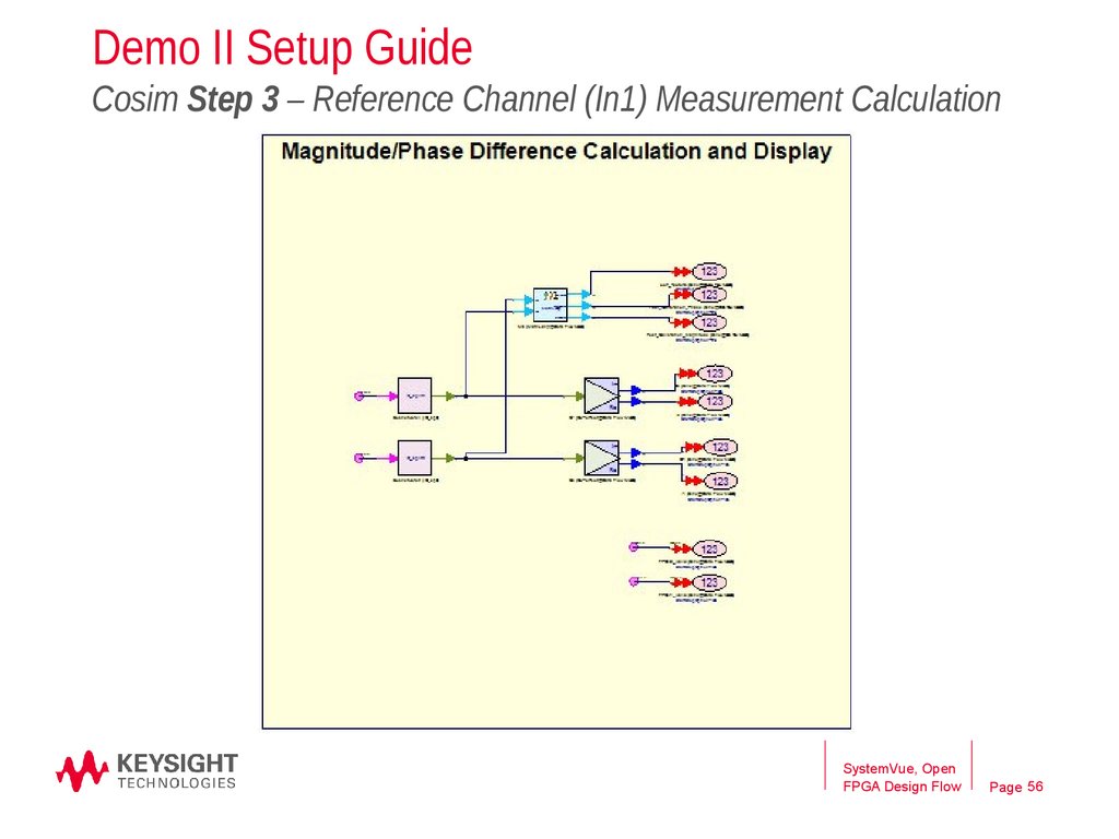
56.
Demo II Setup GuideCosim Step 3 – Reference Channel (In1) Measurement Calculation
SystemVue, Open
FPGA Design Flow
Page 56
57. Demo II Setup Guide Cosim Step 3 – Reference Channel (In1) Magnitude
SystemVue, OpenFPGA Design Flow
Page 57
58. Demo II Setup Guide Cosim Step 3 – Reference Channel (In1) Phase
SystemVue, OpenFPGA Design Flow
Page 58
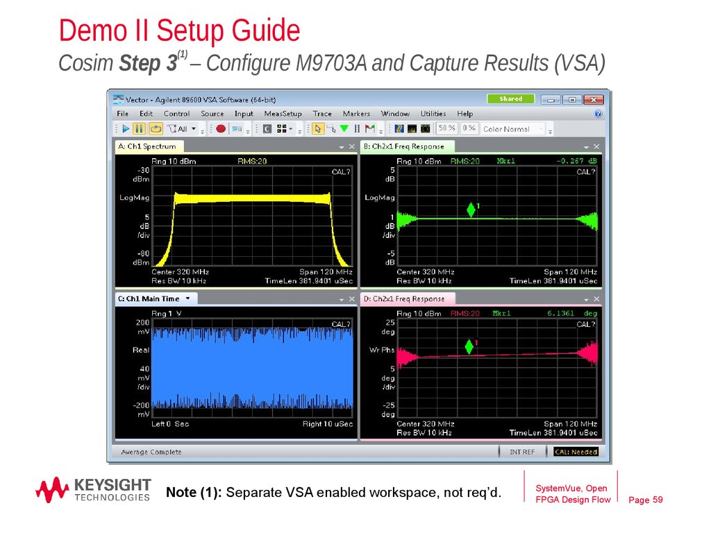
59.
Demo II Setup Guide(1)
Cosim Step 3 – Configure M9703A and Capture Results (VSA)
Note (1): Separate VSA enabled workspace, not req’d.
SystemVue, Open
FPGA Design Flow
Page 59
60. Demo II Setup Guide Cosim Step 4 – Source Configuration
1. SW simulation step only (no HW)2. Source M8190 configuration
3. M9703 measurement + calculate filter coefficients for
reference channel (In1)
4. Source M8190 signal generation
5. M9703 compensation applied to target channel (In3)
SystemVue, Open
FPGA Design Flow
Page 60
61. Demo II Setup Guide Cosim Step 4 – M8190 Source Setup
Sinusoid Sources(Step 2)
M8190
Source
Chirped Source
(Step 4)
SystemVue, Open
FPGA Design Flow
Page 61
62. Demo II Setup Guide Cosim Step 5 – Target Channel (Corrected) Measurement
1. SW simulation step only (no HW)2. Source M8190 configuration
3. M9703 measurement + calculate filter coefficients for
reference channel (In1)
4. Source M8190 signal generation
5. M9703 compensation applied to target channel (In3)
SystemVue, Open
FPGA Design Flow
Page 62
63. Demo II Setup Guide Cosim Step 5 – M9703A Cosim Model
SystemVue, OpenFPGA Design Flow
Page 63
64. Demo II Setup Guide Cosim Step 5 – M9703A UI Parameters (Setup Errors)
SystemVue, OpenFPGA Design Flow
Page 64
65. Demo II Setup Guide Cosim Step 5 – M9703A FPGA Path Correction
SystemVue, OpenFPGA Design Flow
Page 65
66. Demo II Setup Guide Cosim Step 5 – M9703A FPGA Path Correction Message
SystemVue, OpenFPGA Design Flow
Page 66
67. Demo II Setup Guide Cosim Step 5 – M9703A FPGA Setup Errors
Default Path (Error)User Path (Cleared)
Note: Drive letter must
be lowercase.
SystemVue, Open
FPGA Design Flow
Page 67
68. Demo II Setup Guide Cosim Step 5 – M9703A FPGA Setup Errors (Cleared)
SystemVue, OpenFPGA Design Flow
Page 68
69. Demo II Setup Guide Cosim Step 5 – M9703A FPGA(0) Programming UI
SystemVue, OpenFPGA Design Flow
Page 69
70. Demo II Setup Guide Cosim Step 5 – M9703A FPGA(1) Programming UI
SystemVue, OpenFPGA Design Flow
Page 70
71. Demo II Setup Guide Cosim Step 5 – Corrected Channel (In3) Magnitude
SystemVue, OpenFPGA Design Flow
Page 71
72. Demo II Setup Guide Cosim Step 5 – Corrected Channel (In3) Phase
SystemVue, OpenFPGA Design Flow
Page 72
73.
Demo II Setup Guide(1)
Cosim Step 5 – Configure M9703A and Capture Results (VSA)
Note (1): Separate VSA enabled workspace, not req’d.
SystemVue, Open
FPGA Design Flow
Page 73
74. Summary
Introduction to SystemVue hardware design kit
General SystemVue hardware design flow
Integrated FPGA design flow demo for M9703A digitizer
SystemVue, Open
FPGA Design Flow
Page 74
75. Thank you Questions yahia_tachwali@keysight.com
BackupSystemVue/FPGA
Flow
Page 76
76. Backup
M9703A DPU FPGA user core interfaceDPU FPGA User Core Interface:
ADC data stream input
Parallel input
Two DDR3 memory
WR: AXI4-Stream
RD: AXI4-Full
QDRII memory
WR: AXI4-Stream
RD: AXI4-Full
PCIe connectivity with backplane via PCIe
switch
AXI4-Full
AXI4-Lite
Inter FPGAs data stream connectivity
AXI4-Stream
Page 77
77. M9703A DPU FPGA user core interface
Early development of Firmware/Software API’sBefore HW arrives
Custom Application and API
C++ Custom Model Builder
Register
Block Reg
DDR MEM
ADC
corr_factor3
IN1
phase_factor3
IN3
FPGA
ADC
MathLang
mag_factor3
DDR MEM
REAL
HARDWARE
M9703_TEMPLATE
SYSTEMVUE
Basic module configuration and control.
Low-level functions for register-based I/O.
Low-level functions for block-transfers to and from the FPGA and
associated memories.
Higher-level APIs for controlling the FPGA
SystemVue, Open
FPGA Design Flow
Page 78
78. Early development of Firmware/Software API’s Before HW arrives
Standard Conforming BasebandStimulus and response metrology
SystemVue “Baseband Verification” Libraries
3G/4G MOBILITY
NETWORKING
LTE-Advanced (Rel 10)
LTE (Rel 8,9)
WCDMA, HSPA+,
CDMA, CDMA2000
GSM, EDGE
WiMAX / 802.15e
WLAN /802.11abgn/ac
60GHz 802.11ad
Custom OFDM
Data type conversion
Floating/Fixed Point
Soft bits demapping
and metric calculation
I_Phase
PORT=2
Path-metric calculation
and selection of
surviving paths
Wordlength=32 [wl_PM] OutputPrecisionMode=User Defined
IntegerWordleng th=18 [intwl_PM] Wordlength=32 [wl_PM]
IsSigned=Signed
IntegerWordleng th=18 [intwl_PM]
BROADCAST &
SATCOMM
Reversing the order
of decoded bitstream to
match the input
dec0
DecisionIn_0
dec1
DecisionIn_1
dec2
DecisionIn_2
dec3
DecisionIn_3
m2
AddrRe
BitsOut
PORT=3
m3
PM_calc_all_T1
AddrWr
RAM
reset
Q_Phase
PORT=1
RevBits Out
Data
PathToRevBits
PM_calc {PM_calc_all_T1}
DownCntRead
m3
WrtEn
OutputPr Depth=
ecisionMode=User
64 [cntlen] Defined
UpCntWrite
1
LOCAL
CONNECTIVITY
Reverse extraction of
decoded bitstream
m2
Wordlength=32 [wl_PM]OutputPrecisionMode=User Defined
IntegerWordleng th=18 [intwl_PM] Wordleng th=32 [wl_PM]
IntegerWordleng th=18 [intwl_PM]
IsSigned=Signed
SystemVue
SystemVue Hardware
Hardware Design
Design
reset
PathToRevBits {PathToRevBits}
D15
D14
D13
0
WPAN / 802.15.3c
802.11ad
Zigbee / 802.15.4
Bluetooth
Available with W1461BP
core environment
DVB-S2/T2, ISDB-T
General Digital Modem
GNSS sat nav
OutputPrecisionMode=User Defined
A
B
Counter
and
reset
0 1
OutputPrecisionMode=User Defined
signals
A?B
CompareOperation=Eq ual
1
En
Rst
0
Direction=Up
OutputPrecisionMode=User Defined
Delay=3
1
En
0
1
OutputPrecisionMode=User
Defined
0
Rst
Direction=Down
OutputPrecisionMode=User Defined
D19
DEFENSE
RADAR: PD, UWB,
FMCW,
SAR, DAR, SFR, MIMO,
Phased Array
SystemVue, Open
FPGA Design Flow
Page 79
79. Standard Conforming Baseband Stimulus and response metrology
Simplify complex post analysisFixed to floating point data conversion
FFT, Filtering, Re-sampling
Time / Frequency domain conversion and plotting
Send out data from SystemVue to user application for further
processing and display
FFT
R1 {ResamplerRC@Data Flow Models}
Length=64
F1 {FFT_Cx@Data Flow Models}
FFTSize=256
Size=256
Direction=Forward
FreqSequence=0-pos-neg
corr_factor3
IN1
phase_factor3
IN3
MathLang
mag_factor3
SystemVue, Open
FPGA Design Flow
Page 80
80. Simplify complex post analysis
Overcome function test limitation of a timing based simulatorTraditional analog functions are being moved
to DSP - DUC, DDC, DDS, Beam Former,
etc…
Need more than timing & logic analysis
How many FPGA designer can see vector
analysis results during HDL coding and
verification in traditional design flow?
RTL Simulator
Keysight 89600 Vector Analysis Software
SystemVue, Open
FPGA Design Flow
Page 81
81. Overcome function test limitation of a timing based simulator
Real world system level simulationMeasurement and verification of an FPGA model requiring
complex metrics in the presence of real world impairments.
FPGA Model
0
C2 {Const@Data Flow Models}
Value=0
VS A_89600B_Sink
angM odDat
scl_out
scaleDat
M r k5
dc_m ar k_sel
dc_m r ksel
Demod & BER
V1 {VSA_89600B_Sink@Data Flow Models}
VSATitle='Simulation output
M r k4
dc_enable
dc_enable
M r k3
sys_dat a
sys_dat a
M r k2
T
11010
t _sys_valid
Spec _RF_TX {SpectrumAnaly zerEnv@Data Flow Models}
ResBW=100Hz
sys_valid
M r k1
DigitalMod
scl_in
t _sys_r d
sys_r ead
sys_addr
sys_addr
Spe c trum Ana ly zer
M r k0
So c k etServerModel
GNCO
Fr eq
B1 {RandomBits @Data Flow Models}
D2 {DigitalMod@Data Flow Models}
ModTy pe=M-ary CPM
M_ary =2 [M_ary]
h=0.7 [h]
FreqPuls e=GMSK [freq_pulse]
L=5 [Lpulse]
BT =0.3
OversampleRatio=40 [OVSR]
BitOrder=MSB
Work Mode=Continuous
Digital I/Q
BB Modulation
S3 {SetSampleRate@Data Flow Models}
SampleRate=240000Hz [SamplingRate]
dig_dat a
r eg_dat a
Phase
t _dig_valid
123
r eg_valid
Sin
t _dig_r d
r eg_r ead
dig_addr
r eg_addr
Cos
S5 {Soc ketServerModel@Soc ketServ er Models}
Port=13441
Server_IP=
scaling=Register Value
CClk
Subnetwork1 {GNCO}
MarkMode0=Toggle on Mark
Mark Mode1=Mark ed Samples
MarkMode2=Toggle on Mark
Mark Mode3=All Samples
Mark Mode4=All Samples
Mark Mode5=All Samples
CDMA
CPM_Wave {Sink @Data Flow Models}
StartStopOption=Samples
BER
C3 {CDMA_BER@CDMA Models}
Ini=8
Phase
Im
Re
Mag
R1 {RectToCx@Data Flow Models}
123
CPM_Phas e {Sink@Data Flow Models}
StartStopOption=Samples
C1 {Cx ToPolar@Data Flow Models}
W1 {WaveForm@Data Flow Models}
Ex plicitValues=(2x 1) [1; 0]V
Offset=0V
Periodic =YES
TCP/IP client and
data streaming
(control channel from Test Exec)
SystemVue, Open
FPGA Design Flow
Page 82
82. Real world system level simulation
A Realistic ExampleMagnitude and phase calibration for multi-channels
Enhanced FPGA architecture with inter FPGA data transfer
Calibration Coef
Page 83