
 electronics
Similar presentations:

")


Basic Logic Gates
1.
Basic Logic GatesLecture 2
Digital Electronics
2.
Course MaterialsAll needed Software and course materials will
be located on Canvas.
◻ Materials that are used in this slides are taken
from the textbook “Digital Electronics A
Practical Approach with VHDL” by William
Kleitz
◻
3.
AnnouncementsOffice Hours
Thursday
11:00 - 13:00
5th Floor, Open Space
4.
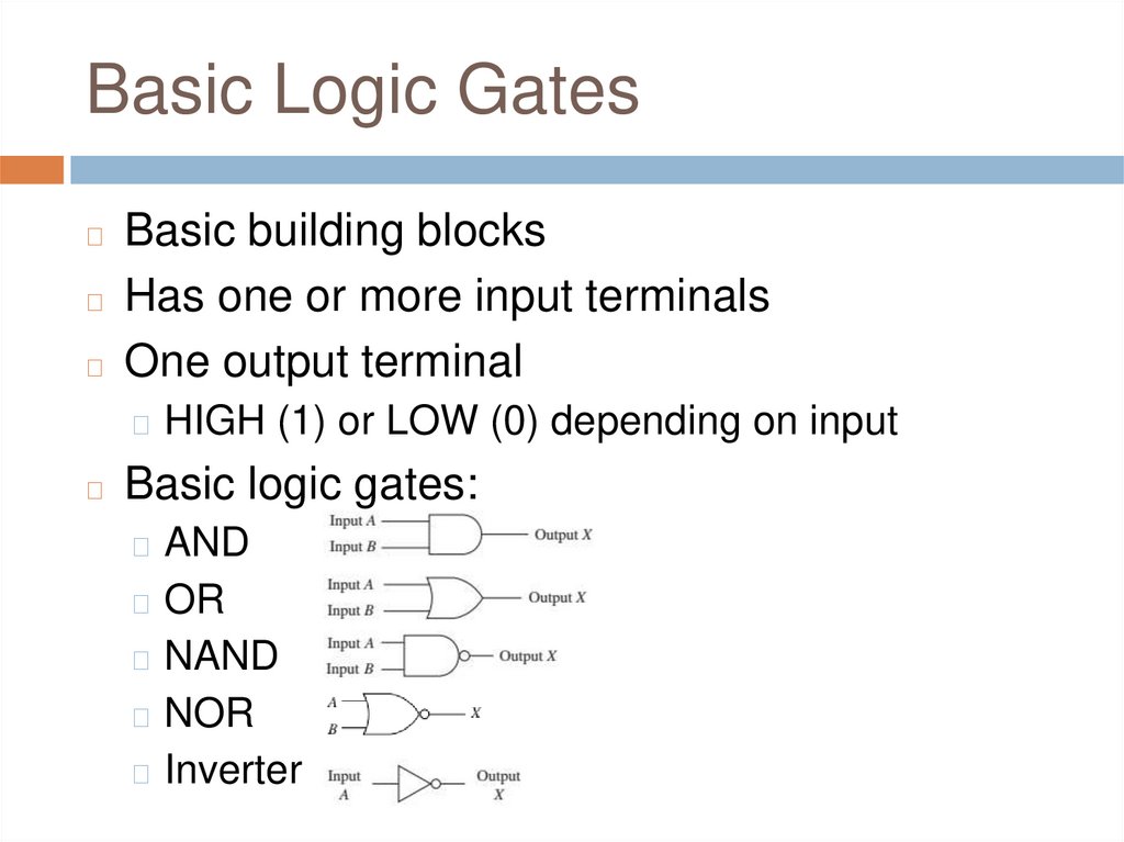
Basic Logic GatesBasic building blocks
◻ Has one or more input terminals
◻ One output terminal
◻
◻ HIGH (1) or LOW (0) depending on input
◻
Basic logic gates:
◻ AND
◻ OR
◻ NAND
◻ NOR
◻ Inverter
5.
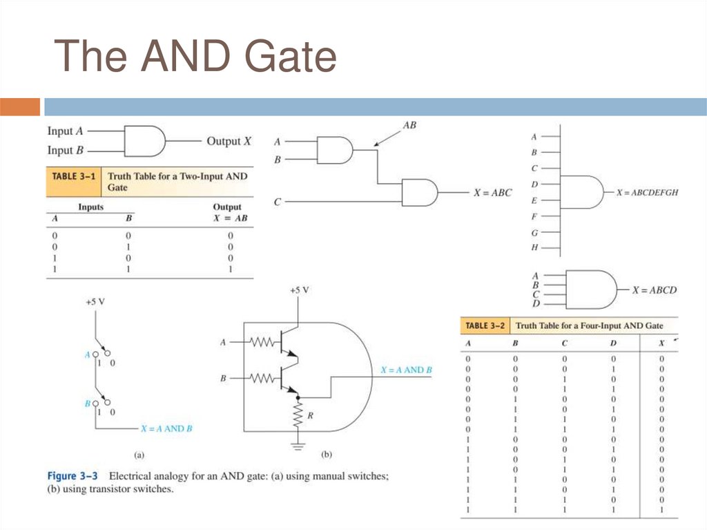
The AND Gate6.
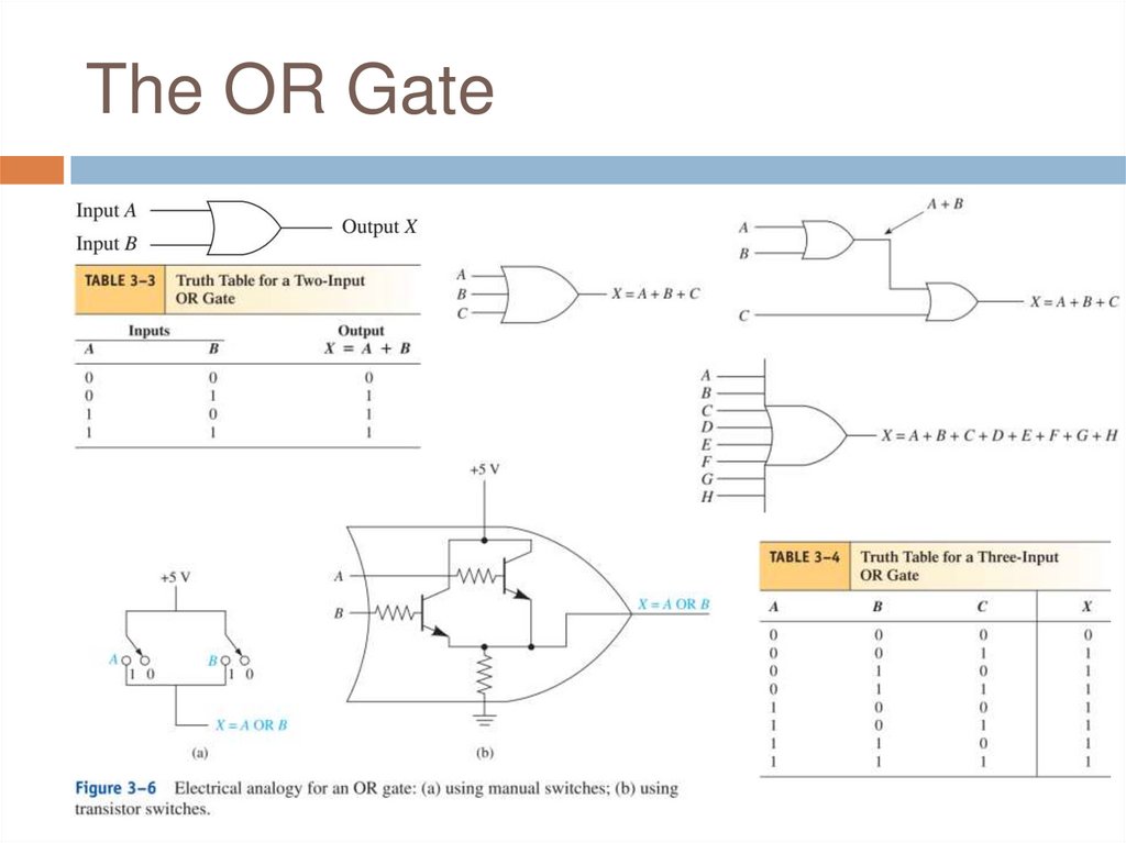
The OR Gate7.
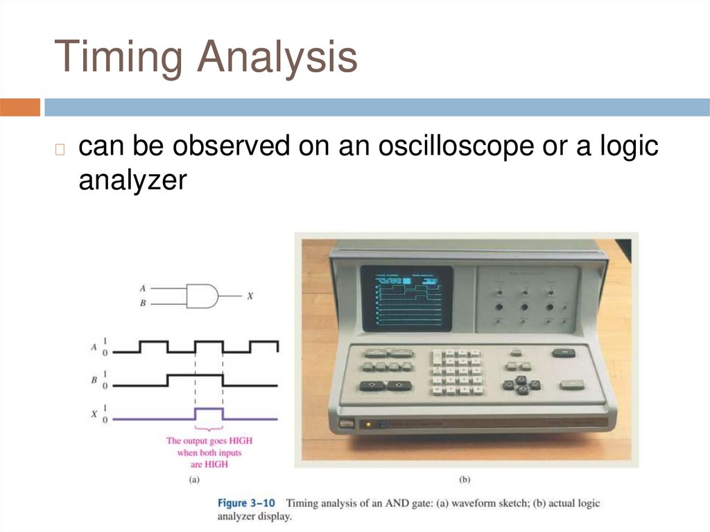
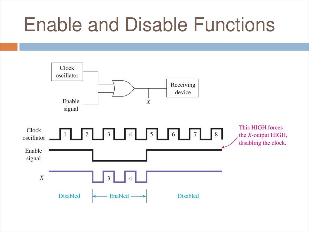
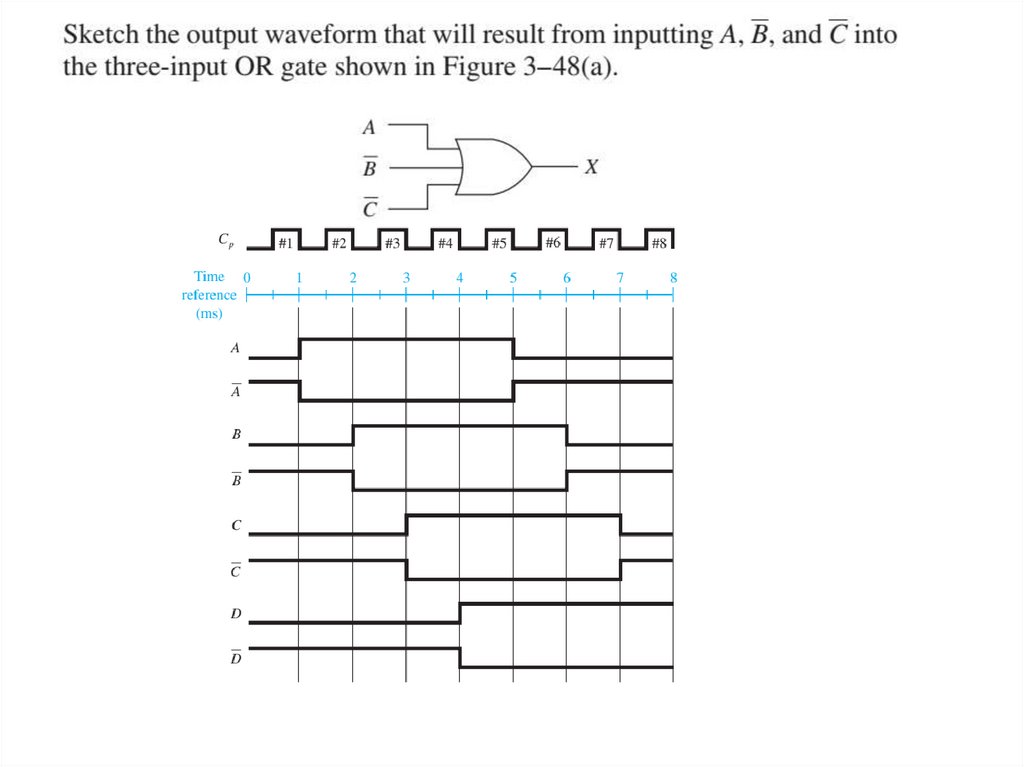
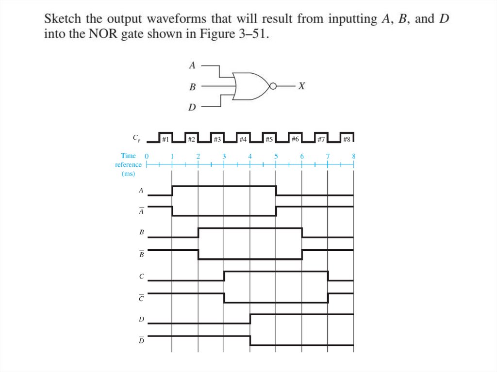
Timing Analysis◻
can be observed on an oscilloscope or a logic
analyzer
8.
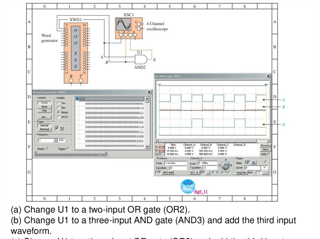
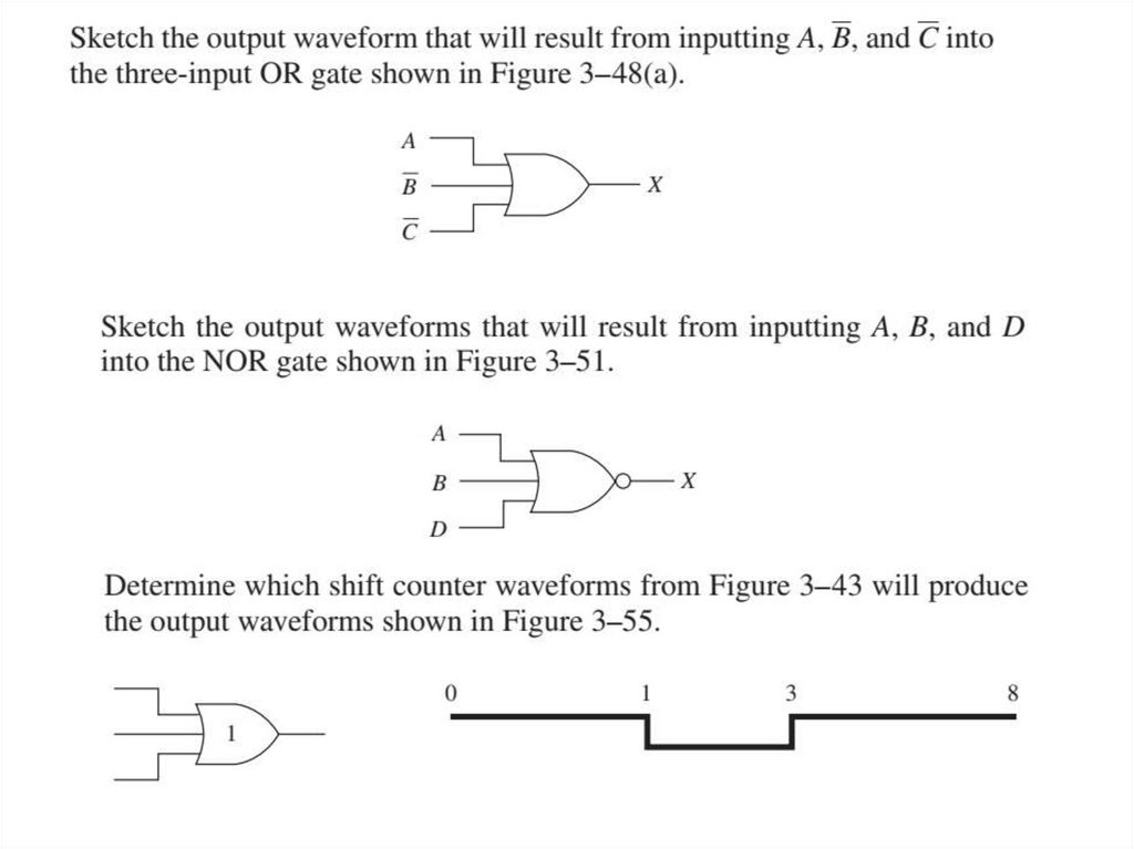
(a) Change U1 to a two-input OR gate (OR2).(b) Change U1 to a three-input AND gate (AND3) and add the third input
waveform.
9.
Enable and Disable Functions10.
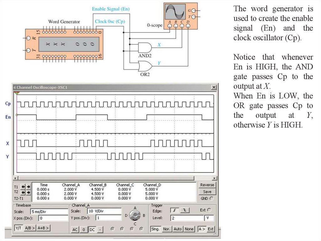
Enable and Disable Functions11.
The word generator isused to create the enable
signal (En) and the
clock oscillator (Cp).
Notice that whenever
En is HIGH, the AND
gate passes Cp to the
output at X.
When En is LOW, the
OR gate passes Cp to
the
output
at
Y,
otherwise Y is HIGH.
12.
Review Questions1.
2.
3.
What input conditions must be satisfied for
the output of an OR gate to be LOW?
A ___________ (HIGH/LOW) level is
required at the input to an AND gate to
enable the signal at the other input to pass to
the output.
What is the purpose of a truth table?
13.
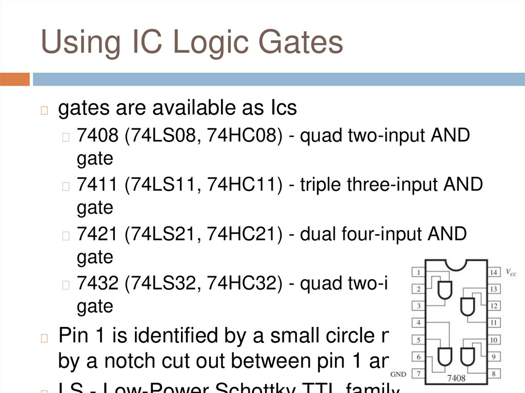
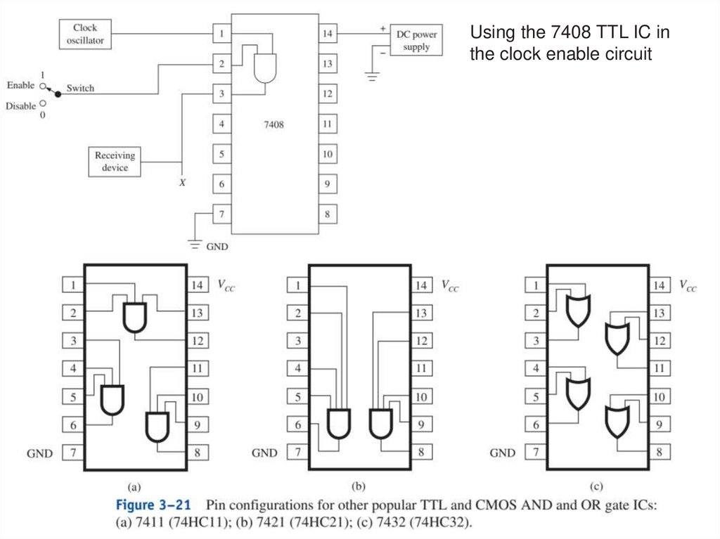
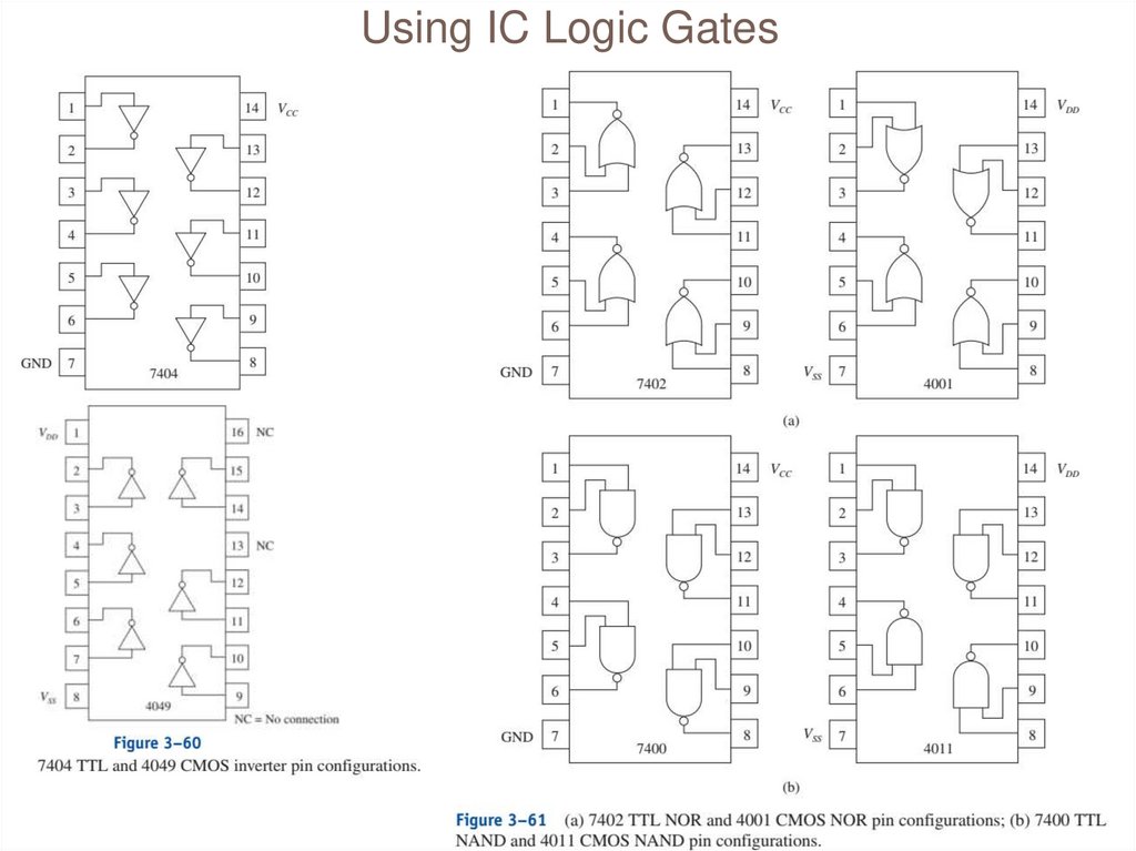
Using IC Logic Gates◻
gates are available as Ics
◻ 7408 (74LS08, 74HC08) - quad two-input AND
gate
◻ 7411 (74LS11, 74HC11) - triple three-input AND
gate
◻ 7421 (74LS21, 74HC21) - dual four-input AND
gate
◻ 7432 (74LS32, 74HC32) - quad two-input OR
gate
◻
Pin 1 is identified by a small circle next to it or
by a notch cut out between pin 1 and 14
14.
Using the 7408 TTL IC inthe clock enable circuit
15.
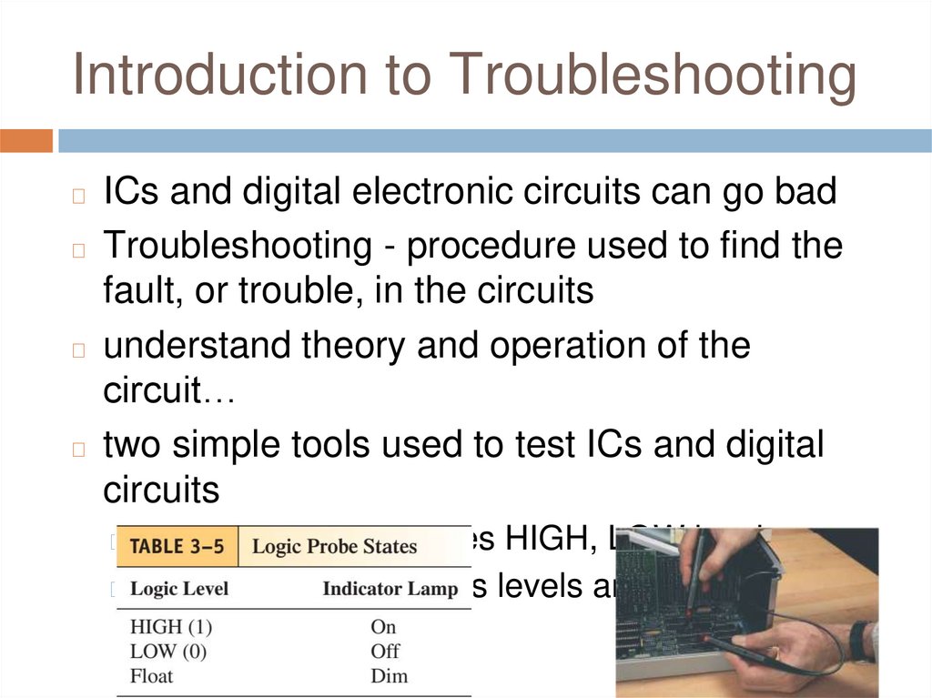
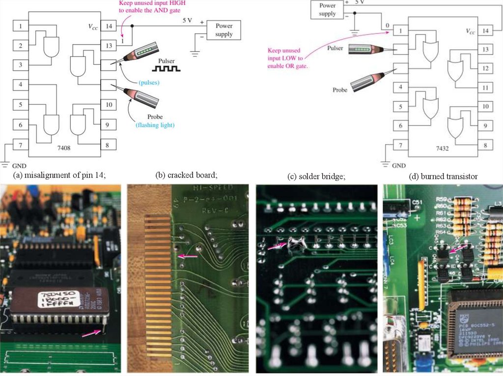
Introduction to TroubleshootingICs and digital electronic circuits can go bad
◻ Troubleshooting - procedure used to find the
fault, or trouble, in the circuits
◻ understand theory and operation of the
circuit…
◻ two simple tools used to test ICs and digital
circuits
◻
◻ logic pulser – generates HIGH, LOW levels
◻ logic probe – measures levels and indicates them
16.
(a) misalignment of pin 14;(b) cracked board;
(c) solder bridge;
(d) burned transistor
17.
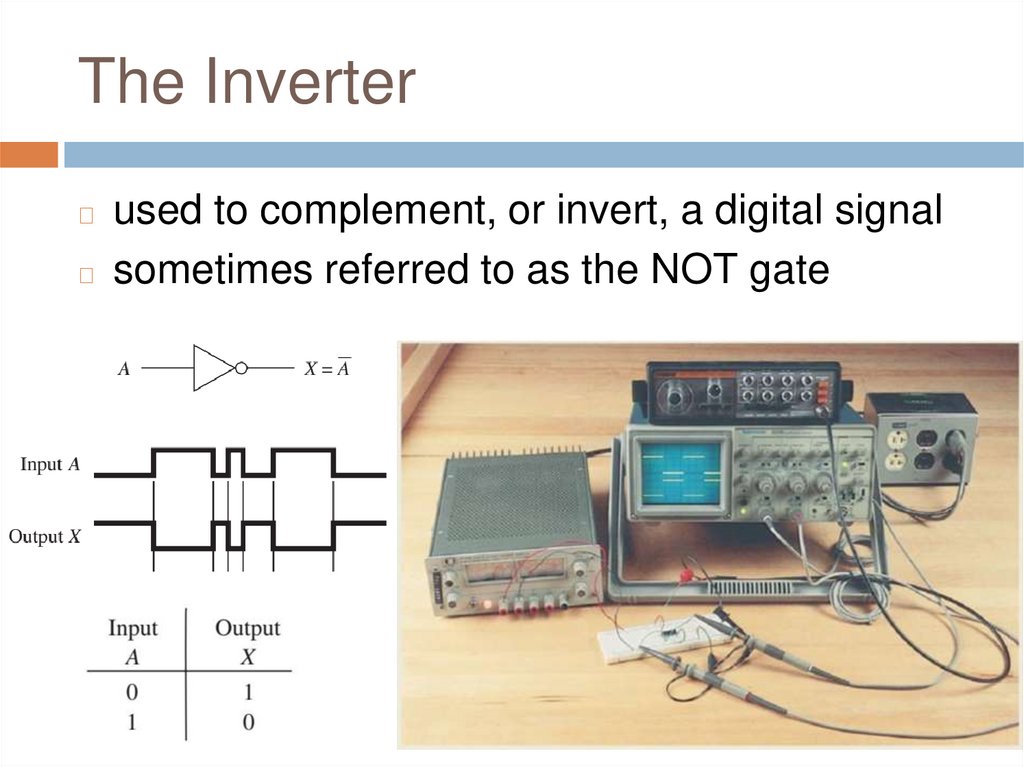
The Inverterused to complement, or invert, a digital signal
◻ sometimes referred to as the NOT gate
◻
18.
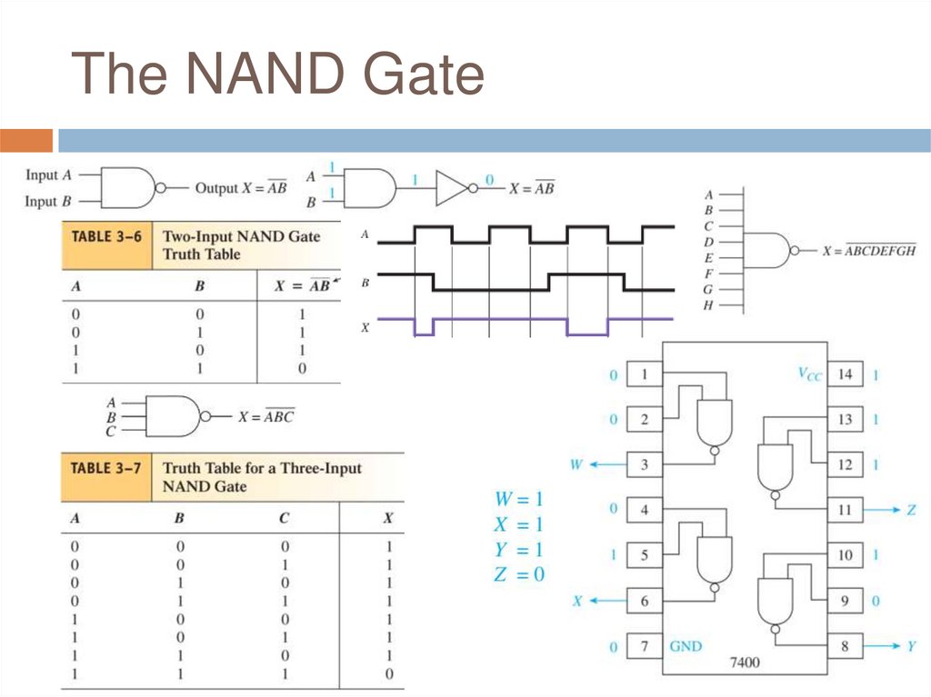
The NAND Gate19.
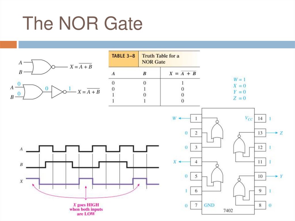
The NOR Gate20.
Review Questions1.
2.
3.
4.
Which pins on the 7408 AND IC are used for
power supply connections, and what voltage
levels are placed on those pins?
What is the purpose of an inverter in a digital
circuit?
The output of a NAND gate is always HIGH
unless all inputs are made ___________
(HIGH/LOW)?
The output of a two-input NOR gate is
___________ (HIGH/LOW) If A = 0, B = 1
21.
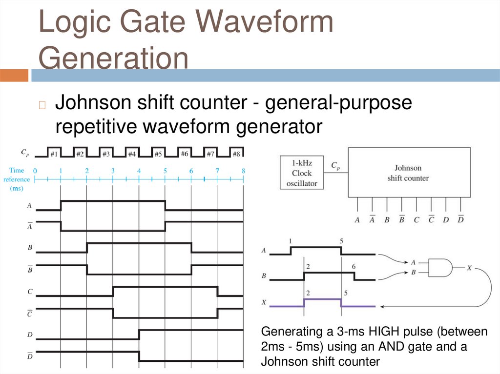
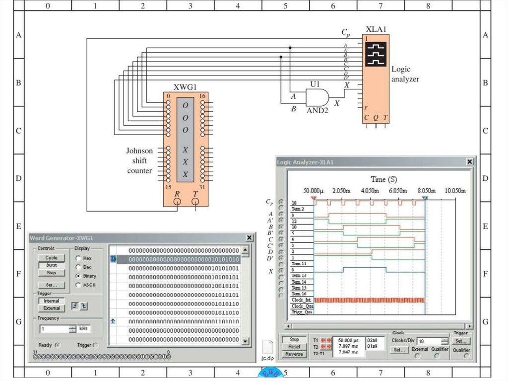
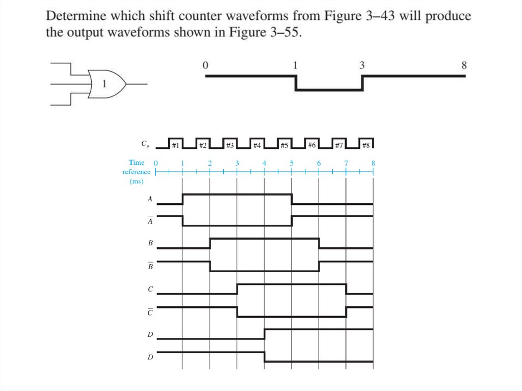
Logic Gate WaveformGeneration
◻
Johnson shift counter - general-purpose
repetitive waveform generator
Generating a 3-ms HIGH pulse (between
2ms - 5ms) using an AND gate and a
Johnson shift counter
22.
23.
24.
25.
26.
27.
Using IC Logic Gates28.
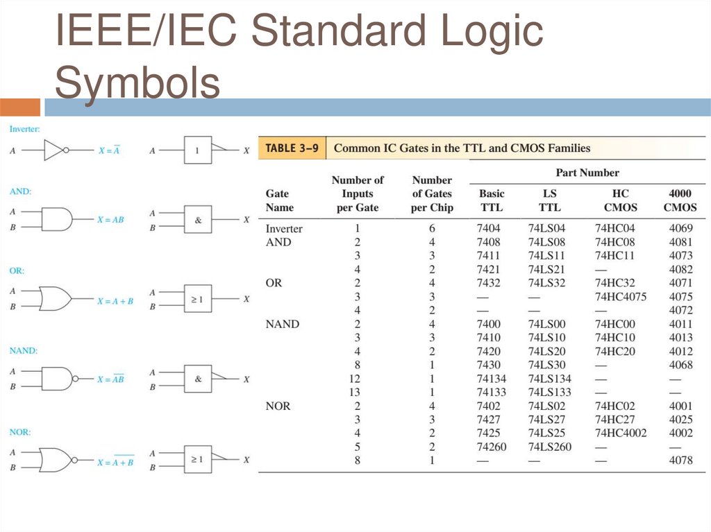
IEEE/IEC Standard LogicSymbols
29.
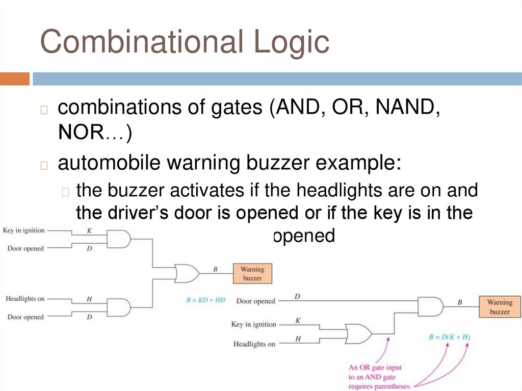
Combinational Logiccombinations of gates (AND, OR, NAND,
NOR…)
◻ automobile warning buzzer example:
◻
◻ the buzzer activates if the headlights are on and
the driver’s door is opened or if the key is in the
ignition and the door is opened
30.
Q&AAny Questions?