


 electronics
Similar presentations:

")


Digital system course. Logic gates
1.
Digital system courseIlyassov Baurzhan, PhD, associate professor,
department of intellectual system and cybersecurity.
2.
Announcement !!!Labs works will be offline at Friday every week.
- For IT-2003 and IT-2004 at 8:30 a.m. at C2-240K
- For IT-2001 and IT-2002 at 10:40 a.m. at C1-348K
Do not miss labs!!!
3.
Homework1. Reading – Chapter 3 of the course book: Digital Electronics:
Principles and Applications 8th Edition by Roger Tokheim, pages 4383
2. Answer to the Chapter Review Questions at the end of the chapter
3, page 83-86.
3. Review Labs 3
Next week it will be the test based on Lecture 3.
4.
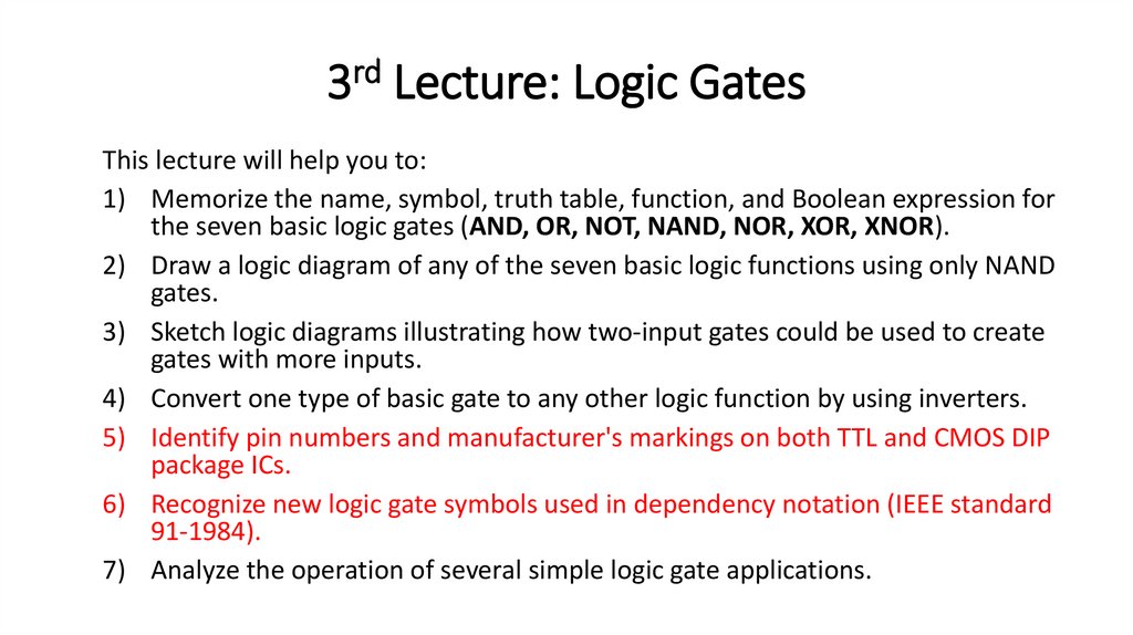
rd3
Lecture: Logic Gates
This lecture will help you to:
1) Memorize the name, symbol, truth table, function, and Boolean expression for
the seven basic logic gates (AND, OR, NOT, NAND, NOR, XOR, XNOR).
2) Draw a logic diagram of any of the seven basic logic functions using only NAND
gates.
3) Sketch logic diagrams illustrating how two-input gates could be used to create
gates with more inputs.
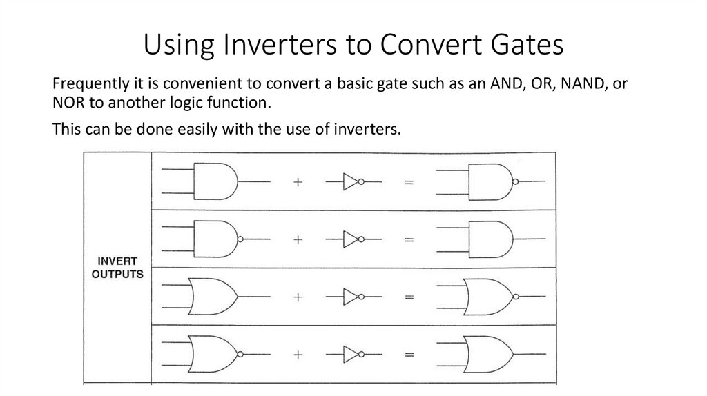
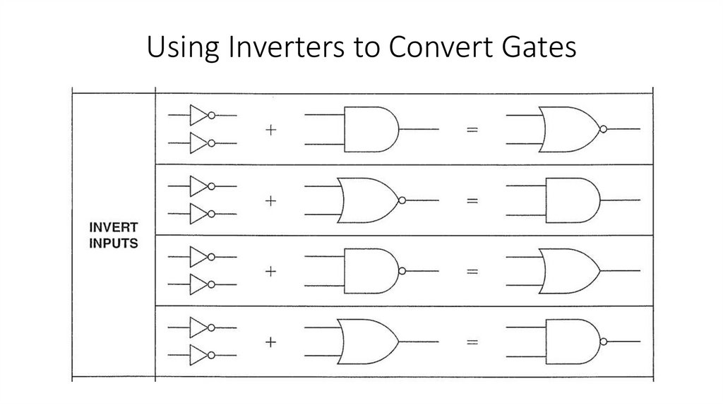
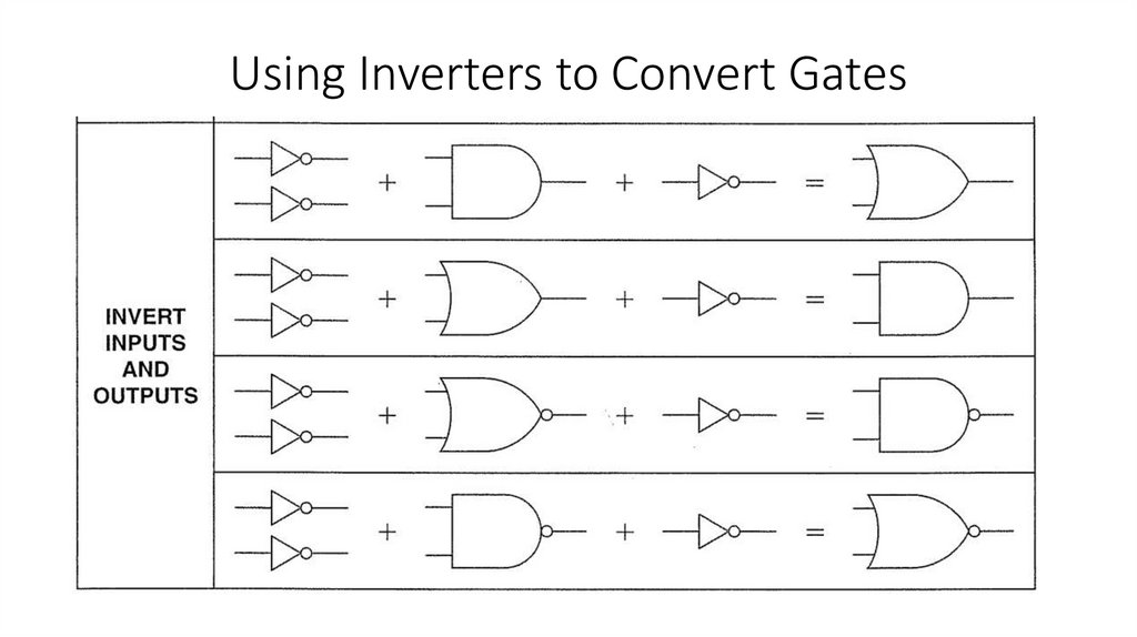
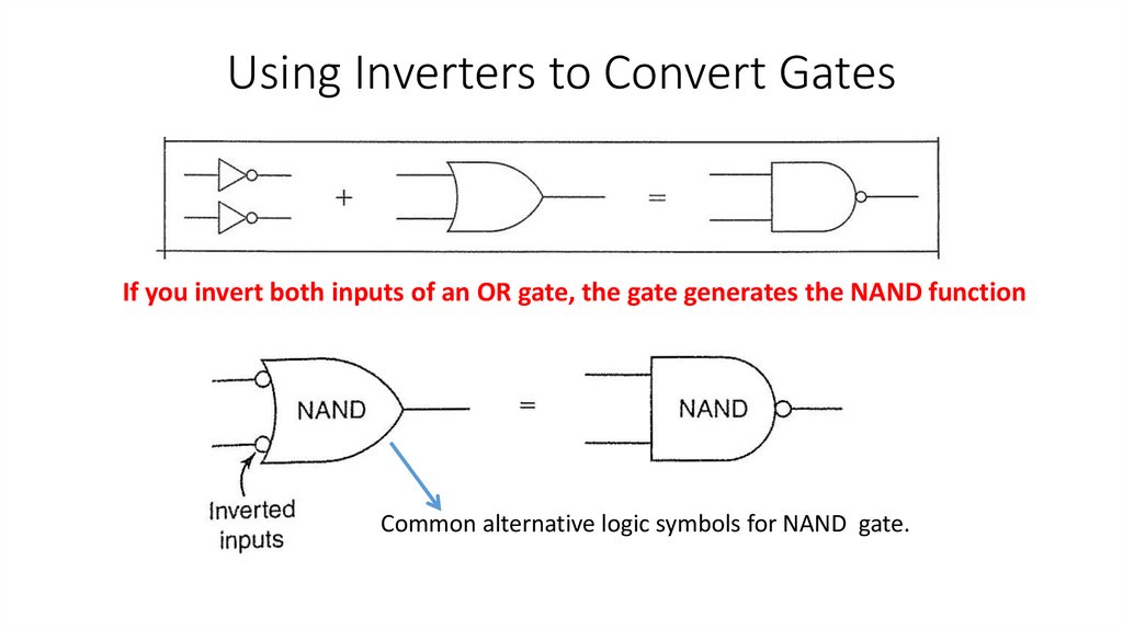
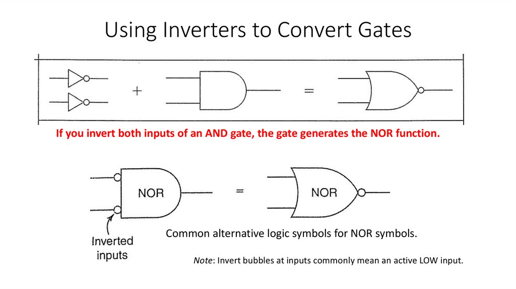
4) Convert one type of basic gate to any other logic function by using inverters.
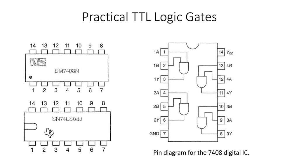
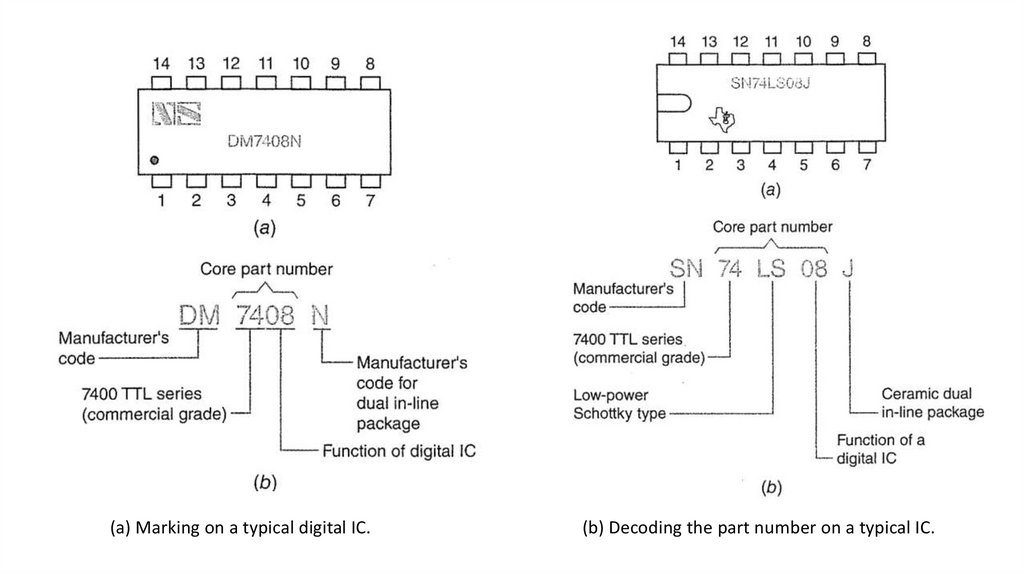
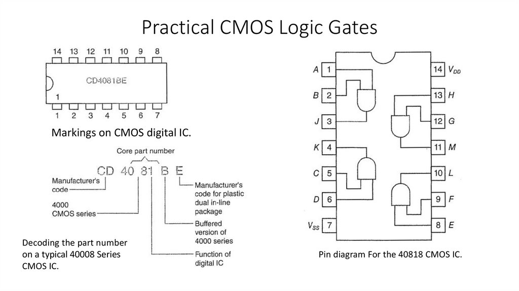
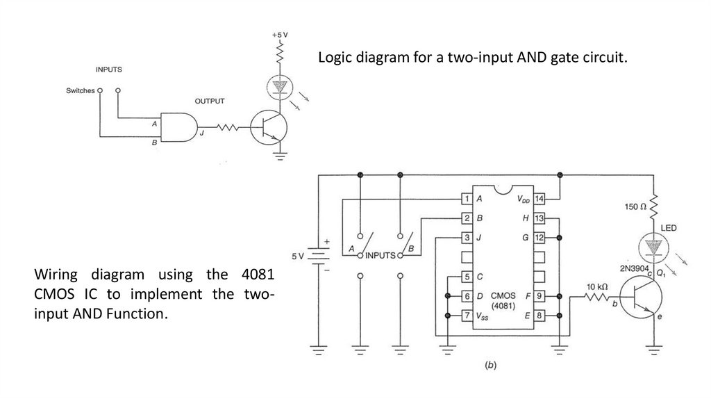
5) Identify pin numbers and manufacturer's markings on both TTL and CMOS DIP
package ICs.
6) Recognize new logic gate symbols used in dependency notation (IEEE standard
91-1984).
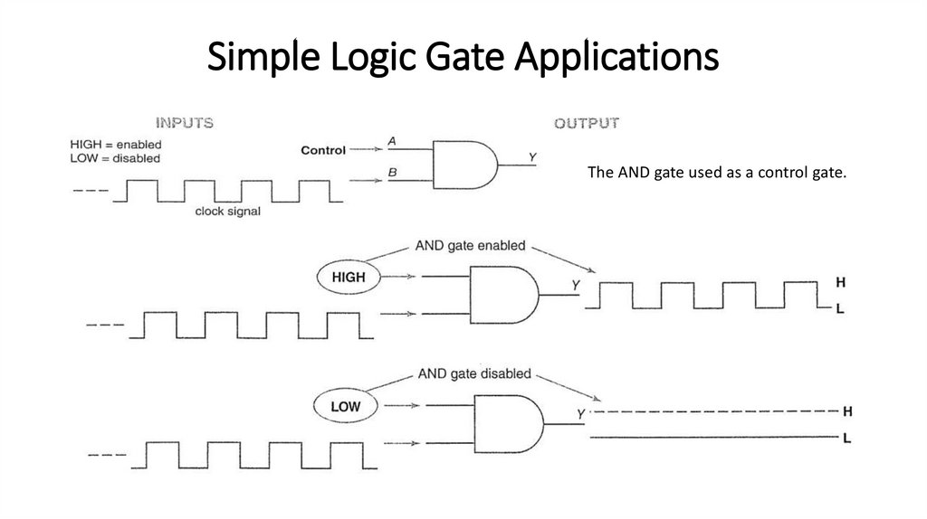
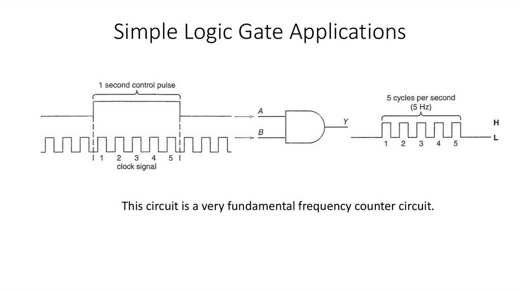
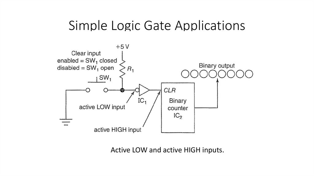
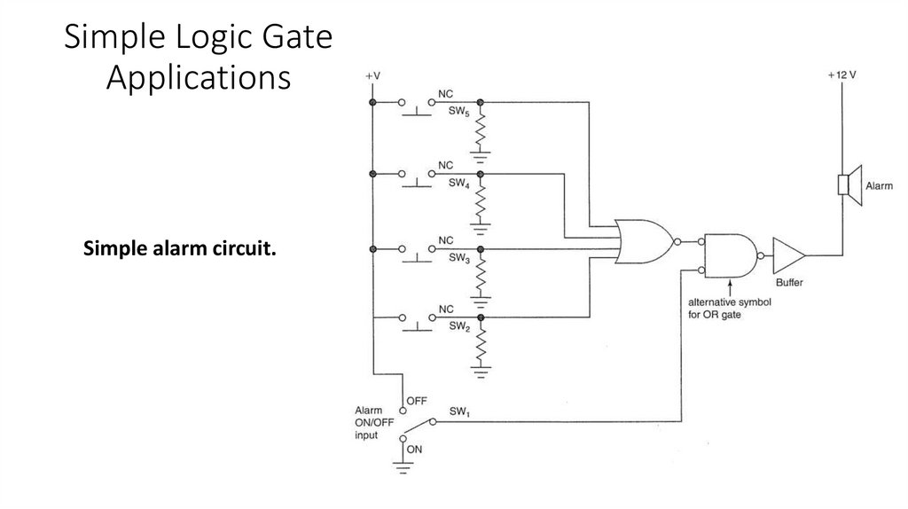
7) Analyze the operation of several simple logic gate applications.
5.
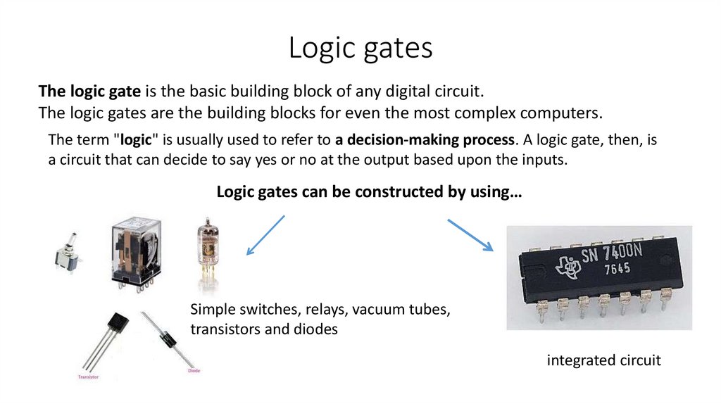
Logic gatesThe logic gate is the basic building block of any digital circuit.
The logic gates are the building blocks for even the most complex computers.
The term "logic" is usually used to refer to a decision-making process. A logic gate, then, is
a circuit that can decide to say yes or no at the output based upon the inputs.
Logic gates can be constructed by using…
Simple switches, relays, vacuum tubes,
transistors and diodes
integrated circuit
6.
Logic gatesThe task performed by a logic gate is called its logic function.
Logic functions can be implemented by
hardware (logic gates)
by programming devices such as
microcontrollers or computers.
7.
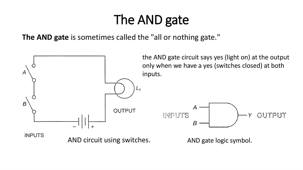
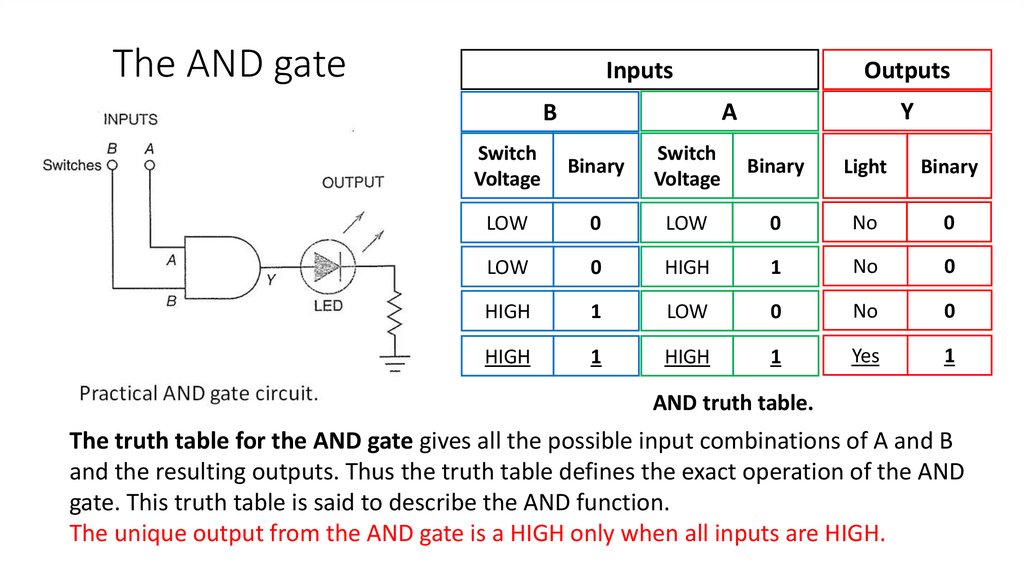
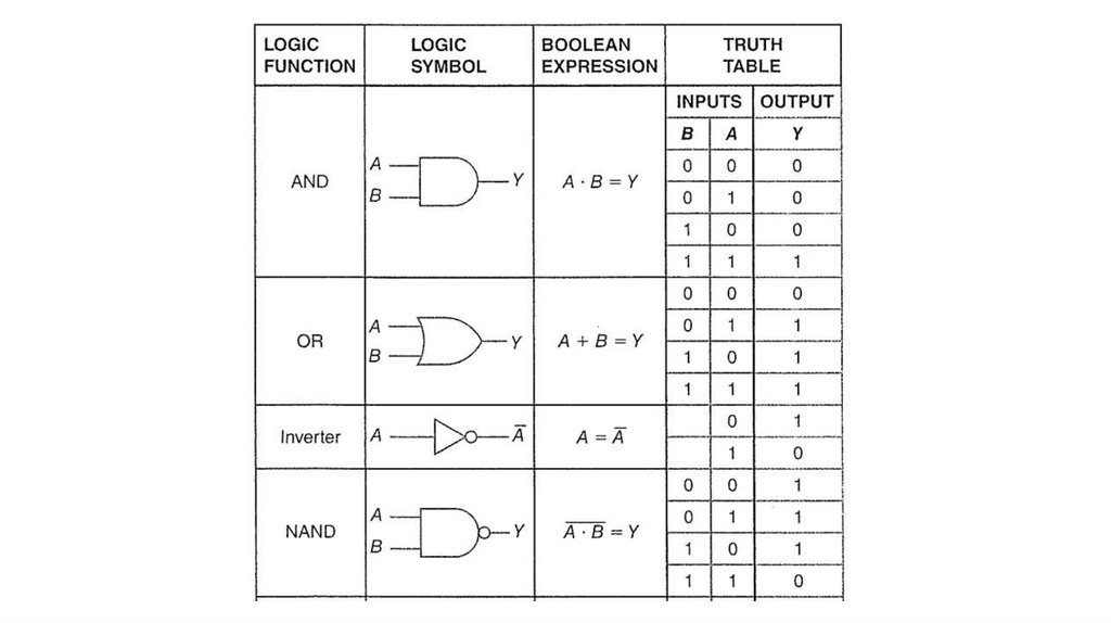
The AND gateThe AND gate is sometimes called the "all or nothing gate."
the AND gate circuit says yes (light on) at the output
only when we have a yes (switches closed) at both
inputs.
AND circuit using switches.
AND gate logic symbol.
8.
The AND gateInputs
Outputs
Y
A
B
Switch
Voltage
Binary
Switch
Voltage
Binary
Light
Binary
LOW
0
LOW
0
No
0
LOW
0
HIGH
1
No
0
HIGH
1
LOW
0
No
0
HIGH
1
HIGH
1
Yes
1
AND truth table.
The truth table for the AND gate gives all the possible input combinations of A and B
and the resulting outputs. Thus the truth table defines the exact operation of the AND
gate. This truth table is said to describe the AND function.
The unique output from the AND gate is a HIGH only when all inputs are HIGH.
9.
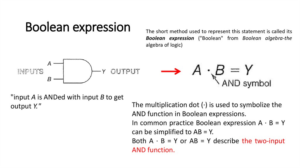
Boolean expression"input A is ANDed with input B to get
output Y."
The short method used to represent this statement is called its
Boolean expression ("Boolean" from Boolean algebra-the
algebra of logic)
The multiplication dot (∙) is used to symbolize the
AND function in Boolean expressions.
In common practice Boolean expression A ∙ B = Y
can be simplified to AB = Y.
Both A ∙ B = Y or AB = Y describe the two-input
AND function.
10.
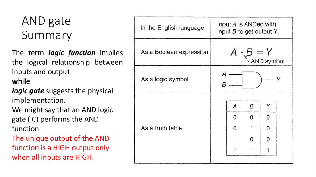
AND gateSummary
The term logic function implies
the logical relationship between
inputs and output
while
logic gate suggests the physical
implementation.
We might say that an AND logic
gate (IC) performs the AND
function.
The unique output of the AND
function is a HIGH output only
when all inputs are HIGH.
11.
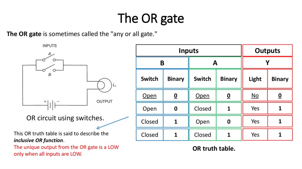
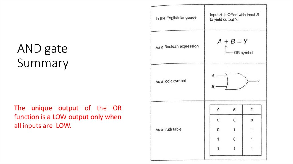
The OR gateThe OR gate is sometimes called the "any or all gate."
Inputs
This OR truth table is said to describe the
inclusive OR function.
The unique output from the OR gate is a LOW
only when all inputs are LOW.
Y
A
B
OR circuit using switches.
Outputs
Switch
Binary
Switch
Binary
Light
Binary
Open
0
Open
0
No
0
Open
0
Closed
1
Yes
1
Closed
1
Open
0
Yes
1
Closed
1
Closed
1
Yes
1
OR truth table.
12.
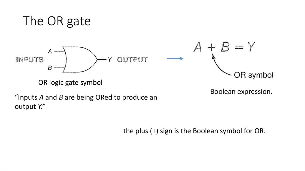
The OR gateOR logic gate symbol
“Inputs A and B are being ORed to produce an
output Y.”
Boolean expression.
the plus (+) sign is the Boolean symbol for OR.
13.
AND gateSummary
The unique output of the OR
function is a LOW output only when
all inputs are LOW.
14.
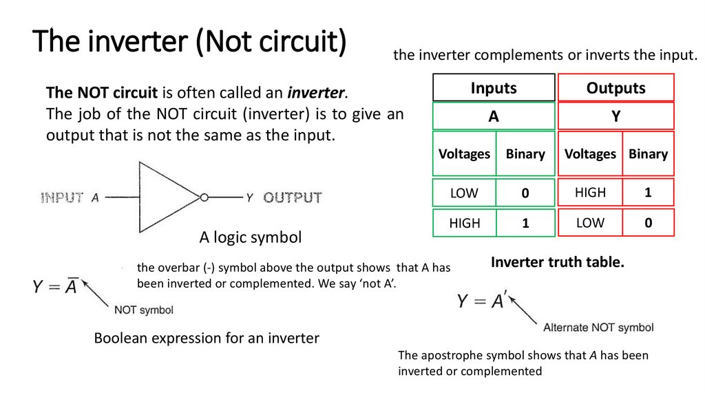
The inverter (Not circuit)the inverter complements or inverts the input.
The NOT circuit is often called an inverter.
The job of the NOT circuit (inverter) is to give an
output that is not the same as the input.
A logic symbol
Inputs
Outputs
A
Y
Voltages
Binary
LOW
0
HIGH
1
HIGH
1
LOW
0
the overbar (-) symbol above the output shows that A has
been inverted or complemented. We say ‘not A’.
Voltages Binary
Inverter truth table.
Boolean expression for an inverter
The apostrophe symbol shows that A has been
inverted or complemented
15.
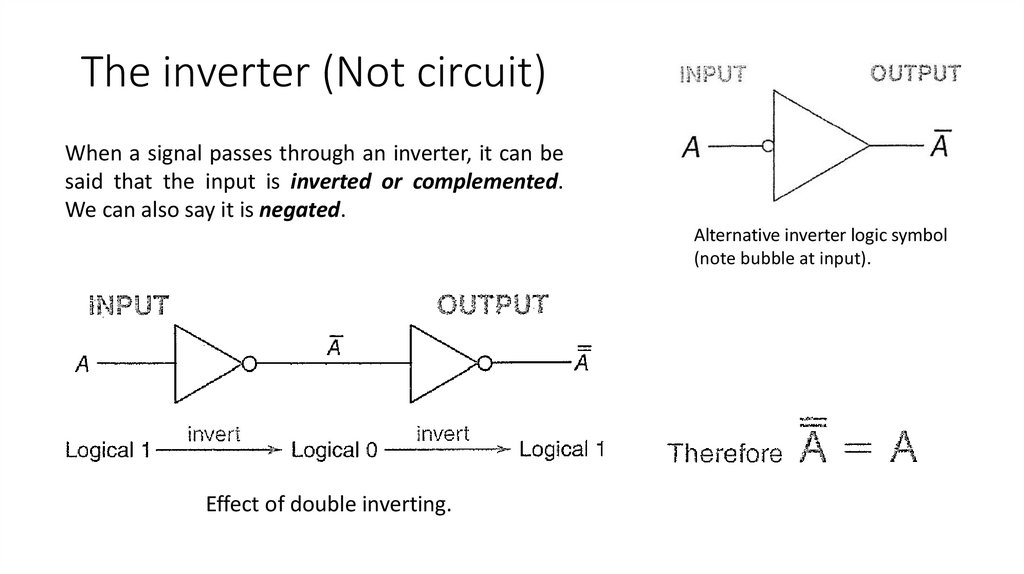
The inverter (Not circuit)When a signal passes through an inverter, it can be
said that the input is inverted or complemented.
We can also say it is negated.
Alternative inverter logic symbol
(note bubble at input).
Effect of double inverting.
16.
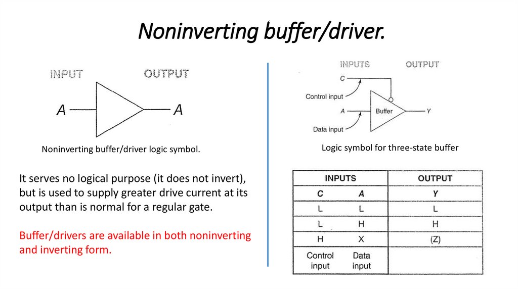
Noninverting buffer/driver.Noninverting buffer/driver logic symbol.
It serves no logical purpose (it does not invert),
but is used to supply greater drive current at its
output than is normal for a regular gate.
Buffer/drivers are available in both noninverting
and inverting form.
Logic symbol for three-state buffer
17.
The NAND GateThe AND, OR, and NOT gates are the three
basic circuits that make up all digital circuits.
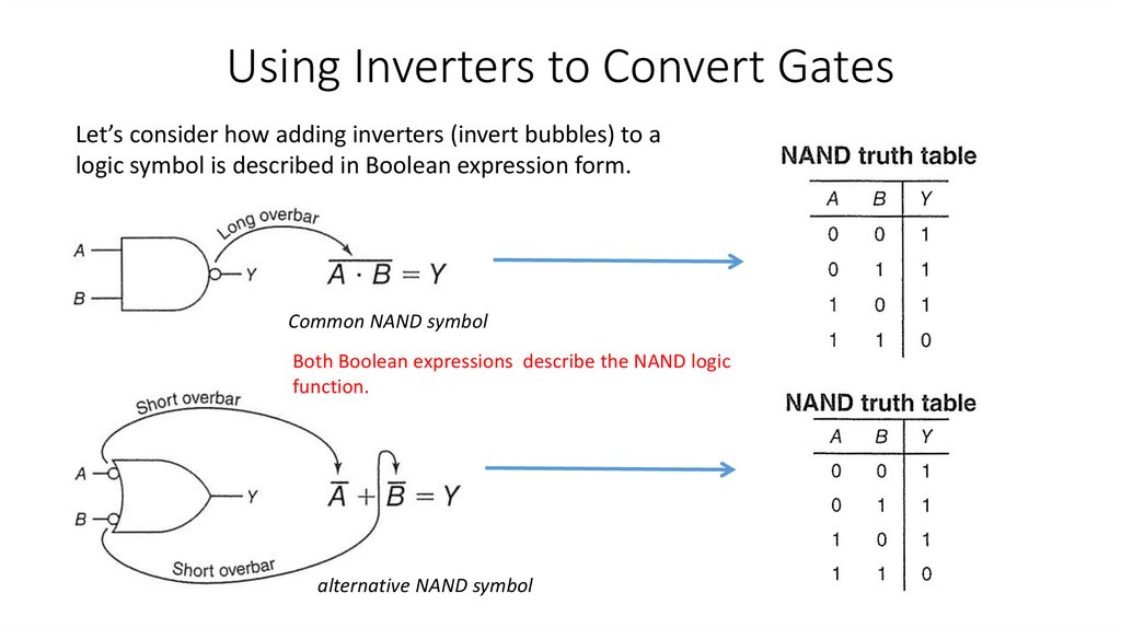
Invert bubble (small circle)
on the right end of the
symbol means to invert the
output of AND.
NAND gate logic symbol.
Truth table for AND and NAND
Output
Inputs
B
A
AND
NAND
0
0
0
1
0
1
0
1
1
0
0
1
1
1
1
0
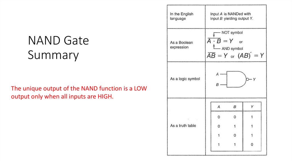
The NAND gate is a NOT AND, or an inverted
AND function.
18.
NAND GateSummary
The unique output of the NAND function is a LOW
output only when all inputs are HIGH.
19.
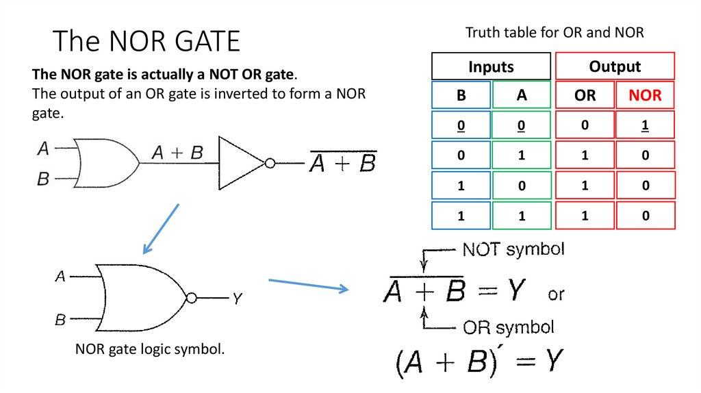
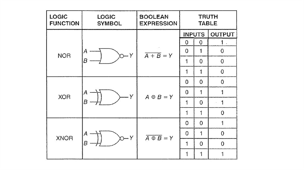
Truth table for OR and NORThe NOR GATE
The NOR gate is actually a NOT OR gate.
The output of an OR gate is inverted to form a NOR
gate.
NOR gate logic symbol.
Output
Inputs
B
A
OR
NOR
0
0
0
1
0
1
1
0
1
0
1
0
1
1
1
0
20.
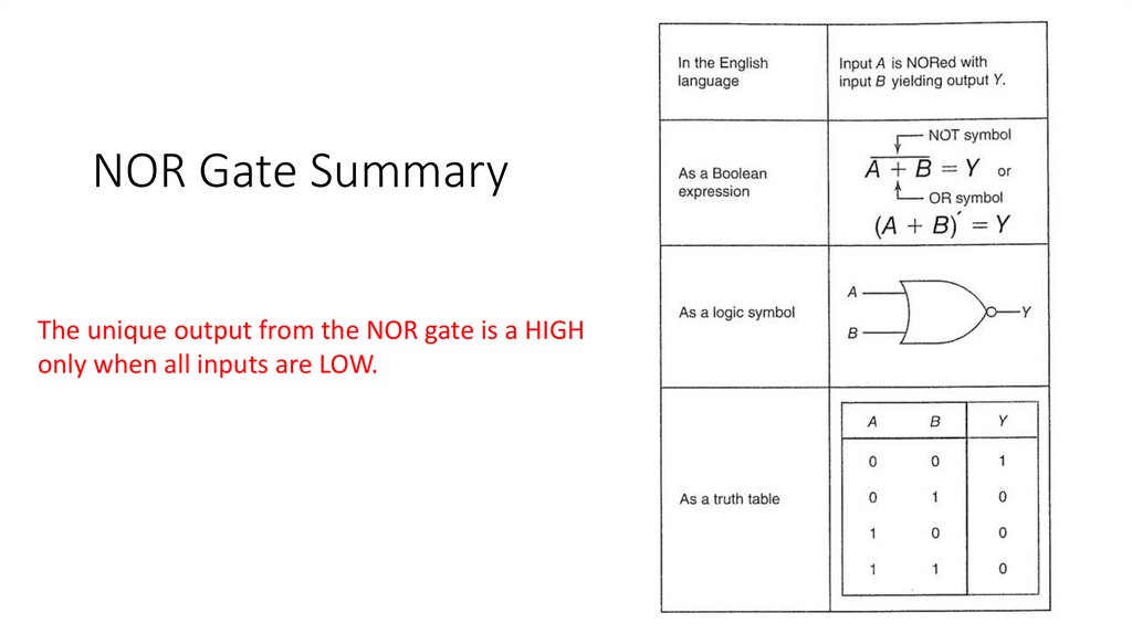
NOR Gate SummaryThe unique output from the NOR gate is a HIGH
only when all inputs are LOW.
21.
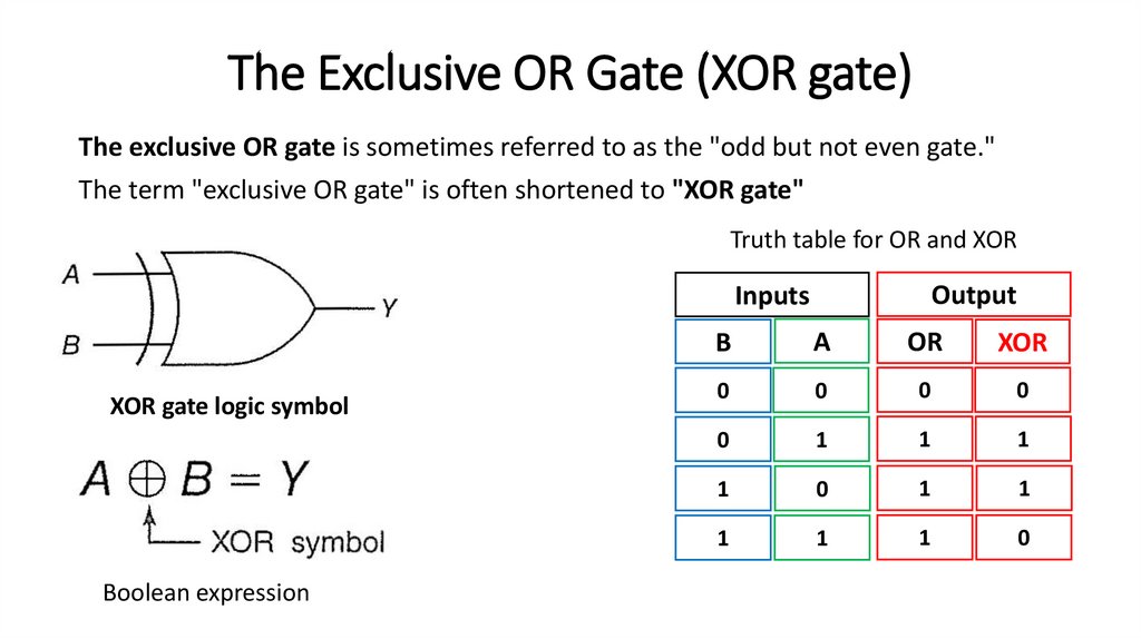
The Exclusive OR Gate (XOR gate)The exclusive OR gate is sometimes referred to as the "odd but not even gate."
The term "exclusive OR gate" is often shortened to "XOR gate"
Truth table for OR and XOR
Output
Inputs
XOR gate logic symbol
Boolean expression
B
A
OR
XOR
0
0
0
0
0
1
1
1
1
0
1
1
1
1
1
0
22.
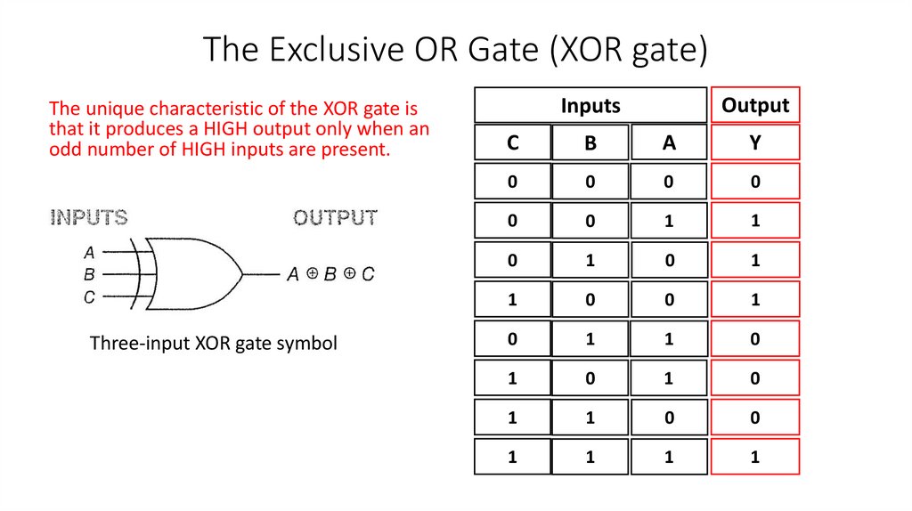
The Exclusive OR Gate (XOR gate)The unique characteristic of the XOR gate is
that it produces a HIGH output only when an
odd number of HIGH inputs are present.
Three-input XOR gate symbol
Output
Inputs
C
B
A
Y
0
0
0
0
0
0
1
1
0
1
0
1
1
0
0
1
0
1
1
0
1
0
1
0
1
1
0
0
1
1
1
1
23.
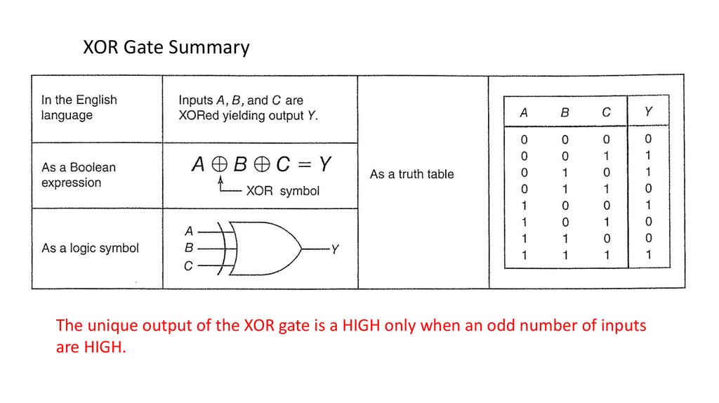
XOR Gate SummaryThe unique output of the XOR gate is a HIGH only when an odd number of inputs
are HIGH.
24.
The Exclusive NOR Gate (XNOR gate)The term "exclusive NOR gate" is often shortened to "XNOR gate."
Truth table for XOR and XNOR
Output
Inputs
XNOR gate logic symbol.
Boolean expression
B
A
XOR
XNOR
0
0
0
1
0
1
1
0
1
0
1
0
1
1
0
1
The unique output of the XNOR gate is a LOW only when an
odd number of inputs are HIGH which is the opposite from the
XOR gate.
25.
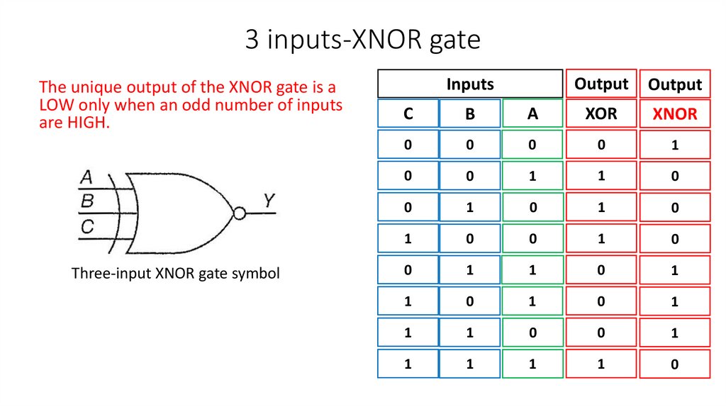
3 inputs-XNOR gateThe unique output of the XNOR gate is a
LOW only when an odd number of inputs
are HIGH.
Three-input XNOR gate symbol
Inputs
Output
Output
C
B
A
XOR
XNOR
0
0
0
0
1
0
0
1
1
0
0
1
0
1
0
1
0
0
1
0
0
1
1
0
1
1
0
1
0
1
1
1
0
0
1
1
1
1
1
0
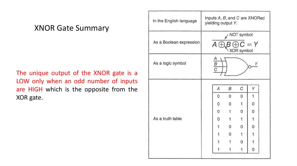
26.
XNOR Gate SummaryThe unique output of the XNOR gate is a
LOW only when an odd number of inputs
are HIGH which is the opposite from the
XOR gate.
27.
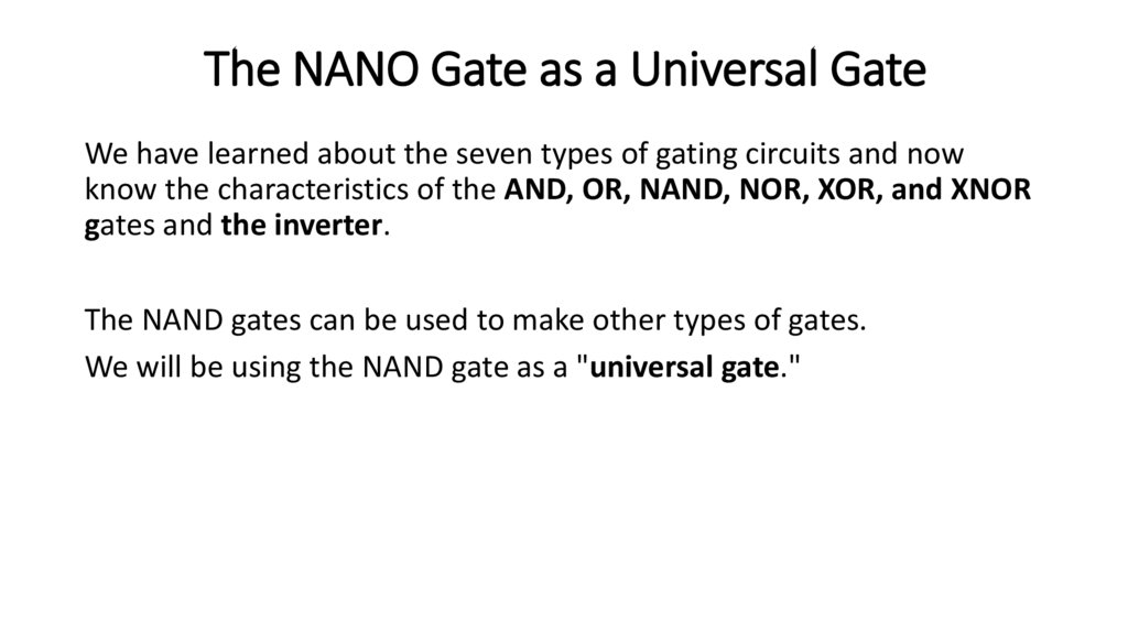
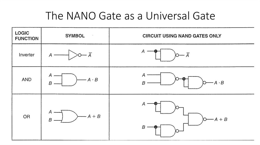
The NANO Gate as a Universal GateWe have learned about the seven types of gating circuits and now
know the characteristics of the AND, OR, NAND, NOR, XOR, and XNOR
gates and the inverter.
The NAND gates can be used to make other types of gates.
We will be using the NAND gate as a "universal gate."
28.
The NANO Gate as a Universal Gate29.
30.
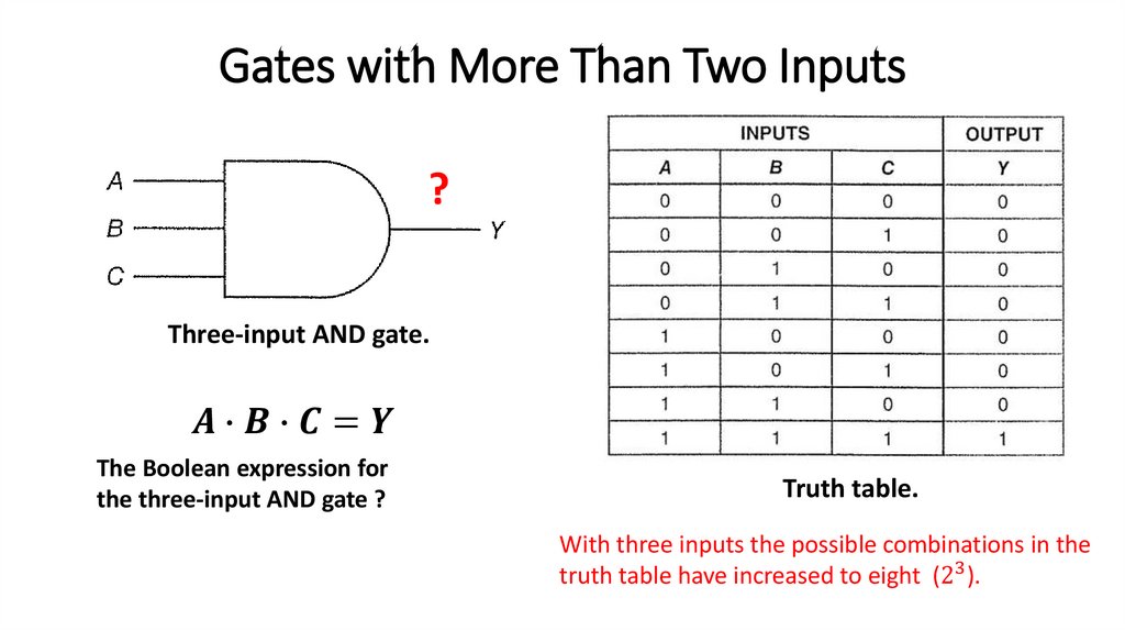
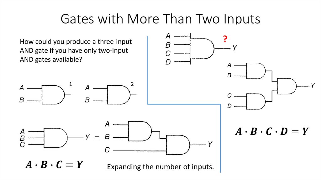
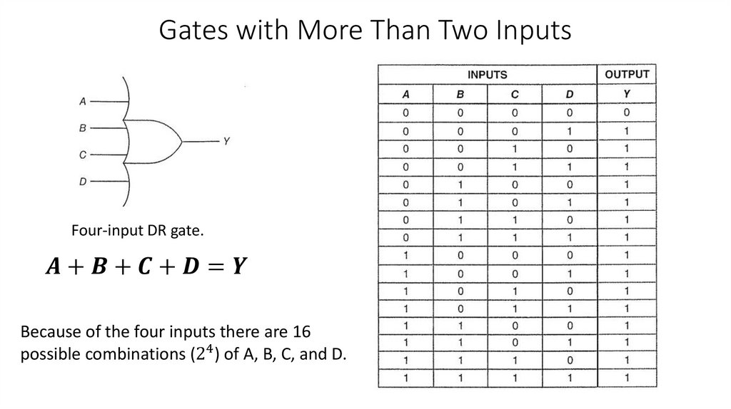
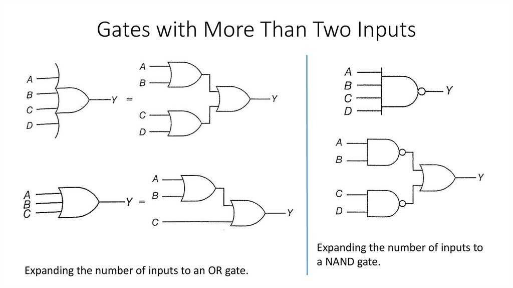
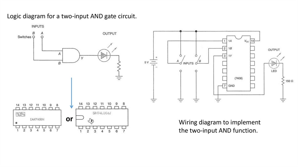
Gates with More Than Two Inputs?
Three-input AND gate.