


 physics
Similar presentations:


Carnelian Р416
1.
ai
l
e
n
r
a
C n
6
1
PDP Training Manual
2.
Agenda1. Introduction to PDP
2. Manufacturing & Structure of Panel
3. PDP Driving Characteristics
4. CARNELIAN Training
5. Trouble shooting
6. CIRCUIT DIAGRAM
3.
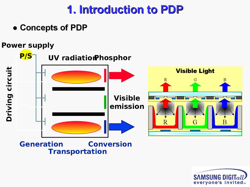
1. Introduction to PDP● Concepts of PDP
Power supply
Driving circuit
P/S
UV radiationPhosphor
Visible Light
R
G
B
R
G
B
Visible
emission
Generation
Conversion
Transportation
4.
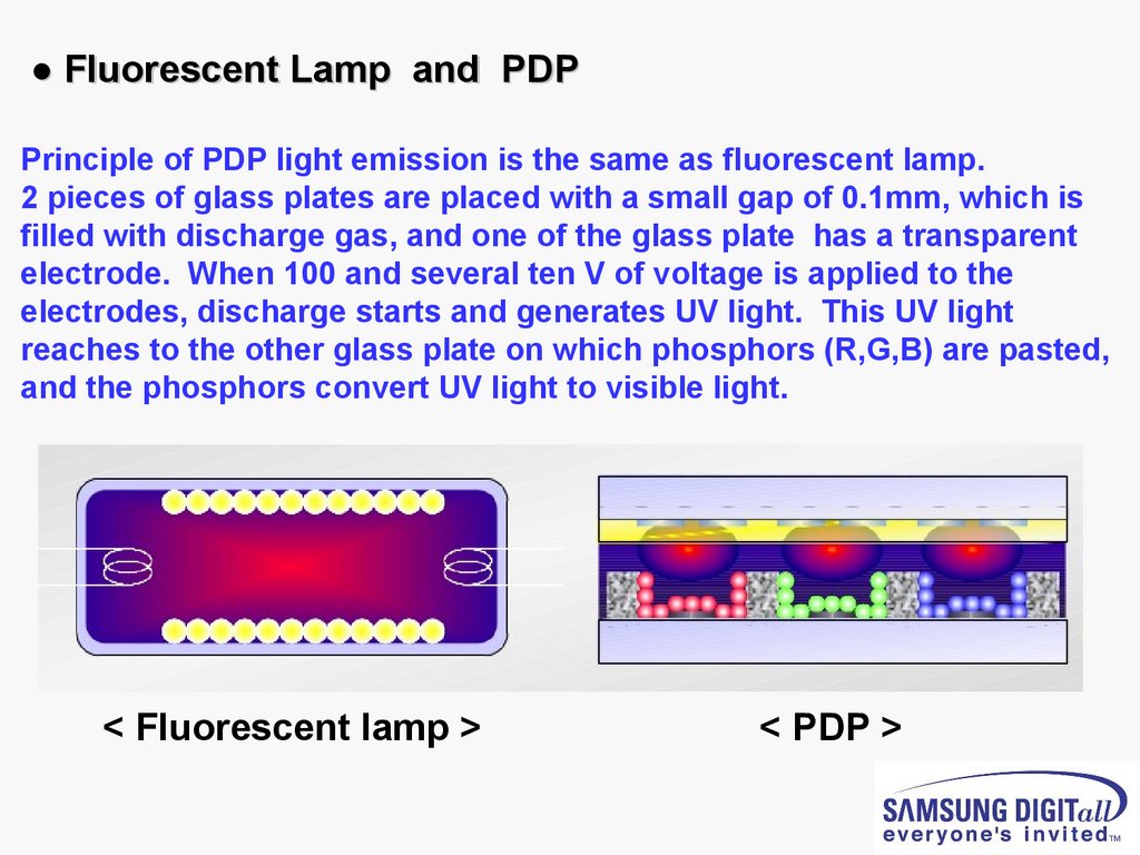
● Fluorescent Lamp and PDPPrinciple of PDP light emission is the same as fluorescent lamp.
2 pieces of glass plates are placed with a small gap of 0.1mm, which is
filled with discharge gas, and one of the glass plate has a transparent
electrode. When 100 and several ten V of voltage is applied to the
electrodes, discharge starts and generates UV light. This UV light
reaches to the other glass plate on which phosphors (R,G,B) are pasted,
and the phosphors convert UV light to visible light.
< Fluorescent lamp >
< PDP >
5.
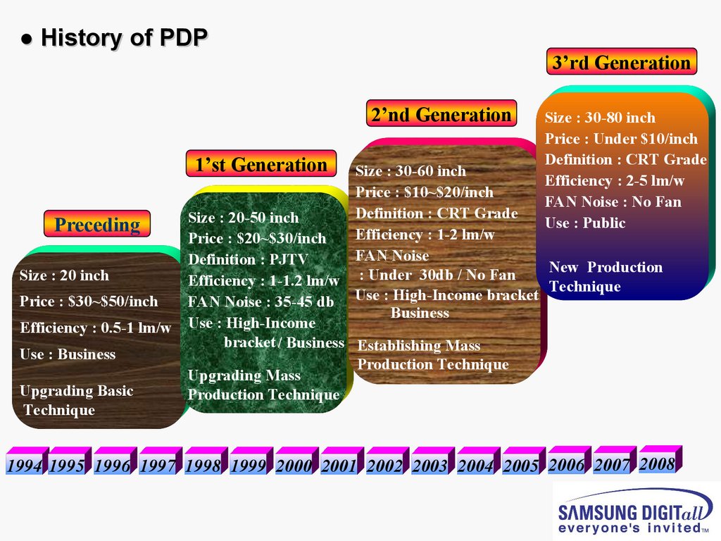
● History of PDP3’rd Generation
2’nd Generation
1’st Generation
Size : 30-80 inch
Price : Under $10/inch
Definition : CRT Grade
Efficiency : 2-5 lm/w
FAN Noise : No Fan
Use : Public
Size : 30-60 inch
Price : $10~$20/inch
Definition : CRT Grade
Size : 20-50 inch
Preceding
Efficiency : 1-2 lm/w
Price : $20~$30/inch
FAN Noise
Definition : PJTV
New Production
:
Under
30db
/
No
Fan
Size : 20 inch
Efficiency : 1-1.2 lm/w
Technique
Use
:
High-Income
bracket
Price : $30~$50/inch
FAN Noise : 35-45 db
Business
Use
:
High-Income
Efficiency : 0.5-1 lm/w
bracket / Business Establishing Mass
Use : Business
Production Technique
Upgrading Mass
Upgrading Basic
Production Technique
Technique
1994 1995 1996 1997 1998 1999 2000 2001 2002 2003 2004 2005 2006 2007 2008
6.
● Merits & Demerits of PDP< Merits
Merits >
>
<
<
< Demerits
Demerits >
>
ThinType
TypeTV
TV
--Thin
LargeScale
Scale::80”
80”possible
possible
--Large
--High
HighPower
PowerConsumption
Consumption
--Low
LowBrightness
Brightness
LightWeight
Weight(42”
(42”Scale)
Scale)
--Light
PDP30kg
30kg//CRT:
CRT:over
over100kg
100kg
::PDP
--High
HighCost
Cost
--Low
LowLighting
LightingEfficiency
Efficiency
LCD40”
40”32Kg
32Kg
::LCD
WideAngleview
Angleview
--Wide
--Image
ImageRetention
Retention
--Operation
OperationTemperature
Temperature
HighDefinition
Definition
--High
cellpitch
pitch0.1mm
0.1mm
::cell
--Acoustic
AcousticNoise
Noiseof
ofDriving
Driving
Not-Sensitiveto
toMagnetic
MagneticField
Field
--Not-Sensitive
Full-color
--Full-color
GoodNon
Nonlinerity
linerity
--Good
Noneed
needfor
forTFT
TFTlike
likeLCD
LCD
::No
7.
Manufacturing &Structure of Panel
8.
2. Manufacturing & Structure of Panel● Cell Structure of Panel
Bus electrode
Front panel
Dielectric
MgO layer
Barrier
Address
Electrode
ITO electrode
Phosphors
Back panel
9.
● Cell Structure of Panel10.
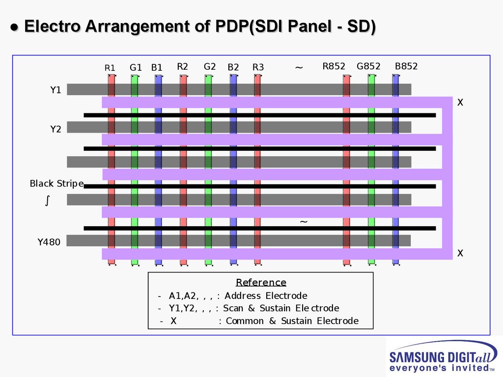
● Electro Arrangement of PDP(SDI Panel - SD)R1
G1 B1
R2
G2
B2
R3
∼
R852
G852
B852
Y1
X
Y2
Black Stripe
∫
∼
Y480
X
Reference
- A1,A2, , , : Address Electrode
- Y1,Y2, , , : Scan & Sustain Ele ctrode
- X
: Common & Sustain Electrode
11.
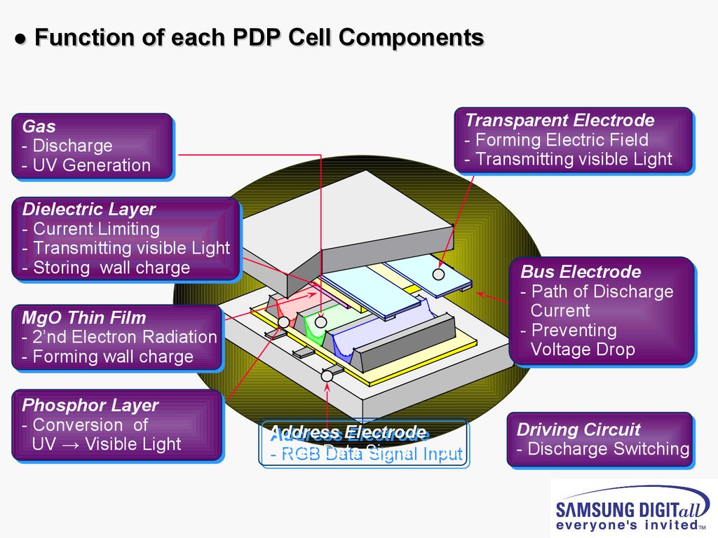
● Function of each PDP Cell ComponentsTransparent
Transparent Electrode
Electrode
-- Forming
Forming Electric
Electric Field
Field
-- Transmitting
Transmitting visible
visible Light
Light
Gas
Gas
-- Discharge
Discharge
-- UV
UV Generation
Generation
Dielectric
Dielectric Layer
Layer
-- Current
Current Limiting
Limiting
-- Transmitting
Transmitting visible
visible Light
Light
-- Storing
Storing wall
wall charge
charge
Bus
Bus Electrode
Electrode
-- Path
Path of
of Discharge
Discharge
Current
Current
-- Preventing
Preventing
Voltage
Voltage Drop
Drop
MgO
MgO Thin
Thin Film
Film
-- 2’nd
2’nd Electron
Electron Radiation
Radiation
-- Forming
Forming wall
wall charge
charge
Phosphor
Phosphor Layer
Layer
-- Conversion
Conversion of
of
UV
UV →
→ Visible
Visible Light
Light
Address
Address Electrode
Electrode
-- RGB
RGB Data
Data Signal
Signal Input
Input
Driving
Driving Circuit
Circuit
-- Discharge
Discharge Switching
Switching
12.
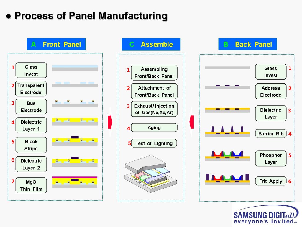
● Process of Panel ManufacturingA Front Panel
1
Glass
Invest
2 Transparent
Electrode
3
4
C Assemble
1
Assembling
Front/Back Panel
Glass
Invest
1
2
Attachment of
Front/Back Panel
Address
Electrode
2
Dielectric
Layer
3
Bus
Electrode
3 Exhaust/ Injection
of Gas(Ne,Xe,Ar)
Dielectric
Layer 1
4
5
Black
Stripe
6
Dielectric
Layer 2
7
MgO
Thin Film
B Back Panel
Aging
Barrier Rib 4
5 Test of Lighting
Phosphor
Layer
5
Frit Apply
6
13.
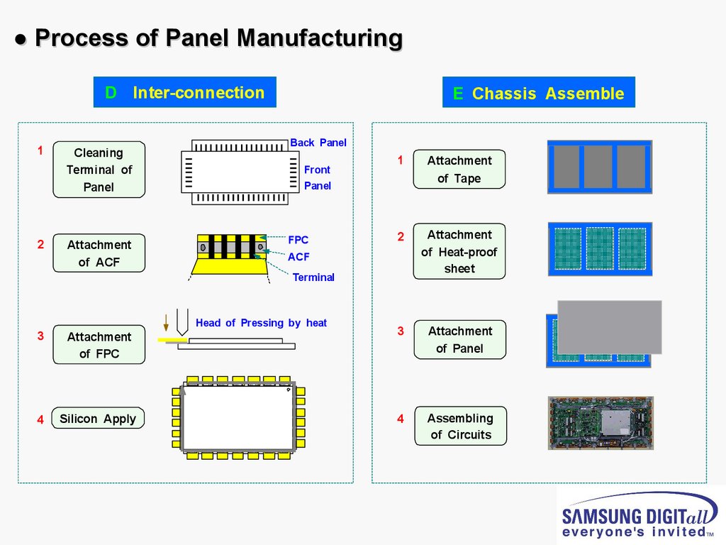
● Process of Panel ManufacturingD Inter-connection
1
2
Cleaning
Terminal of
Panel
Attachment
of ACF
E Chassis Assemble
Back Panel
Front
1
Attachment
of Tape
2
Attachment
of Heat-proof
sheet
Panel
FPC
ACF
Terminal
Head of Pressing by heat
3
Attachment
of FPC
3
Attachment
of Panel
4
Silicon Apply
4
Assembling
of Circuits
14.
PDP DrivingCharacteristics
15.
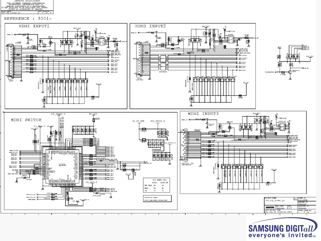
3. General PDP Driving Characteristics● Function Description by board - 1
■.SMPS(Switching Mode Power Supply)
: It is the supplier to provide voltage and current to work the drive voltage and panel in each board.
■.X-MAIN BOARD
: It makes the drive wave form by switching FETs to Timing Controlle coming from logic-board and
supplies X electrode of panel with the drive wave form via connector.
■.Y-MAIN BOARD
: It makes the drive wave form by switching FETs to Timing Controller coming from the logic-board
and provides Y electrode of panel with the drive wave form via Scan Driver IC on Y buffer board
in order.
■.LOGIC MAIN BOARD
: It process image signal and performs buffering of the logic-main board (to create XY drive signal
and output) and the address driver output signal.
Then it supplies the output signal to the address driver IC(COF Module).
16.
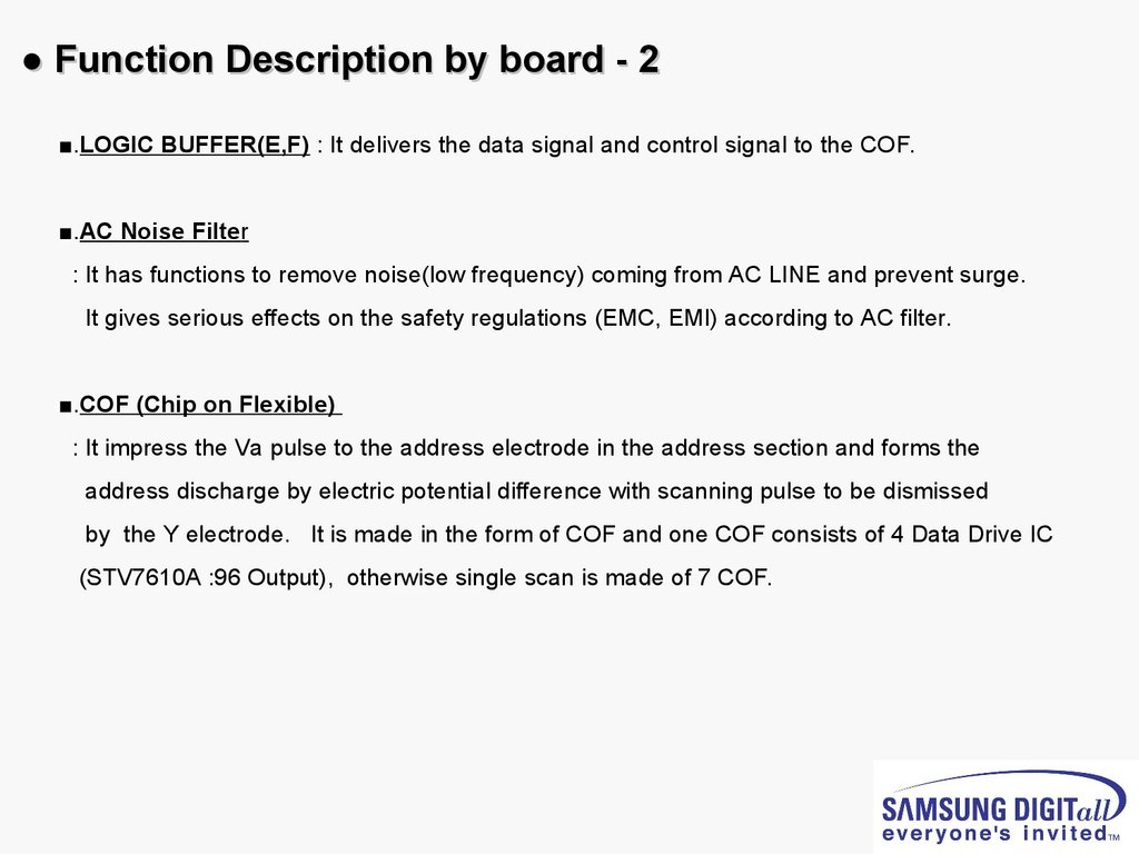
● Function Description by board - 2■.LOGIC BUFFER(E,F) : It delivers the data signal and control signal to the COF.
■.AC Noise Filter
: It has functions to remove noise(low frequency) coming from AC LINE and prevent surge.
It gives serious effects on the safety regulations (EMC, EMI) according to AC filter.
■.COF (Chip on Flexible)
: It impress the Va pulse to the address electrode in the address section and forms the
address discharge by electric potential difference with scanning pulse to be dismissed
by the Y electrode. It is made in the form of COF and one COF consists of 4 Data Drive IC
(STV7610A :96 Output), otherwise single scan is made of 7 COF.
17.
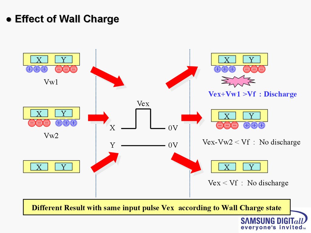
● Effect of Wall ChargeY
X
X
Y
Vw1
Vex+Vw1 >Vf : Discharge
Vex
Y
X
Vw2
X
Y
X
X
0V
Y
0V
Y
Vex-Vw2 < Vf : No discharge
X
Y
Vex < Vf : No discharge
Different Result with same input pulse Vex according to Wall Charge state
18.
● 1 Sub-Field Image Process(ADS – Address Data Separate)Reset
Function
Function
••Sustain
SustainErase
Erase
••Wall
WallCharge
ChargeSet
Set
Issue
Issue
••Operation
Operationmargin
margin
••Contrast
Contrast
••Short
ShortTime
Time
Address
Sustain
Function
Function
••Select
SelectOn
OnCell
Cell
Function
Function
••Discharge
DischargeOn
OnCell
Cell
Issue
Issue
••High
HighSpeed
Speed
••Low
LowVoltage
Voltage
••Low
LowFailure
Failure
Issue
Issue
••High
HighEfficiency
Efficiency
••Low
LowVoltage
Voltage
••ERC
ERCPerformance
Performance
19.
● Driving Waveform Specification (P3 Alexander)Reset
Address
Sustain
Y rising
Y sustain
Ramp
Pulse
Y falling
Ramp
Y scan
Pulse
X sustain
Pulse
Address
Pulse
A1,2.....
X
Y1,2....
Address(=Data) Electrode
Vs
85V
Ve
110V
Common & Sustain Electrode
Vset
95V
Va
79V
Scan & Sustain Electrode
Vscan
85V
20.
● Address OperationIn
Inorder
orderto
todisplay
displaypicture,
picture,
select
selectthe
thecells.
cells.
21.
● Sustain OperationDisplay
Displaycells
cellsthrough
throughstrong
strong
Sustain
Sustaindischarge.
discharge.
22.
● Combination of R,G,B Light1 - Pixel
Level of Luminance
RED 4096 Levels
Green 4096 Levels Blue 4096 Levels
68.7 Billion Colors
23.
● Luminance ControlNumber
of Pulses
1
2
4
2048
Lights
1
2
4
2048
24.
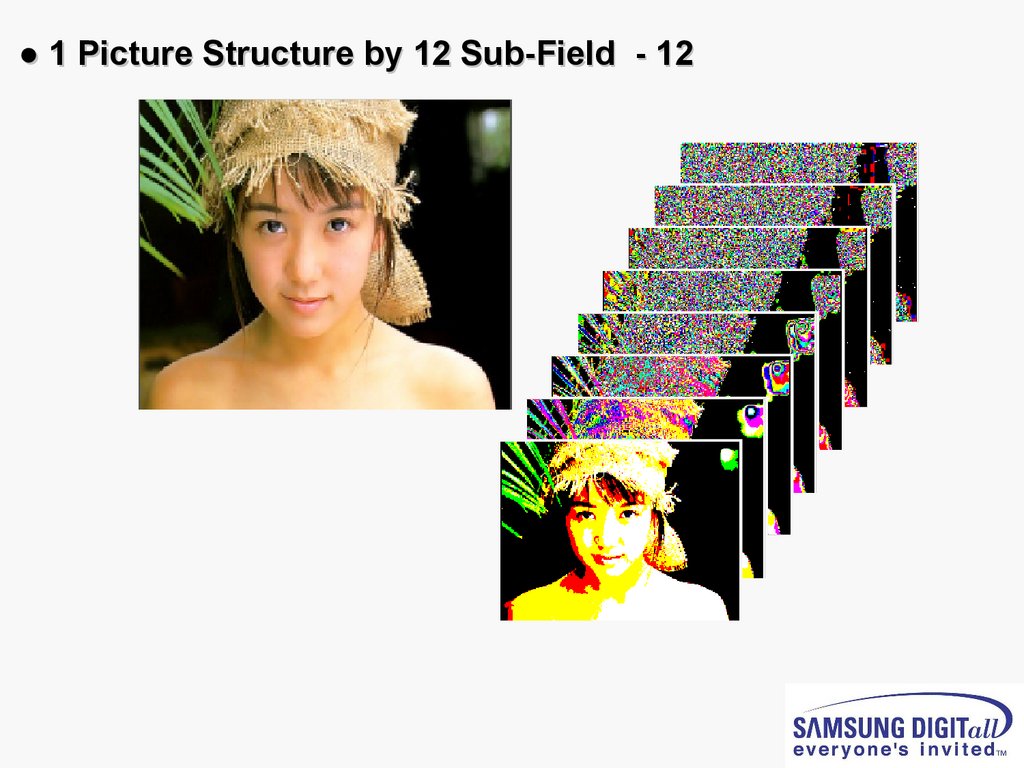
● 1 Picture Structure by 12 Sub-Field - 125.
● 1 Picture Structure by 12 Sub-Field - 226.
● 1 Picture Structure by 12 Sub-Field - 327.
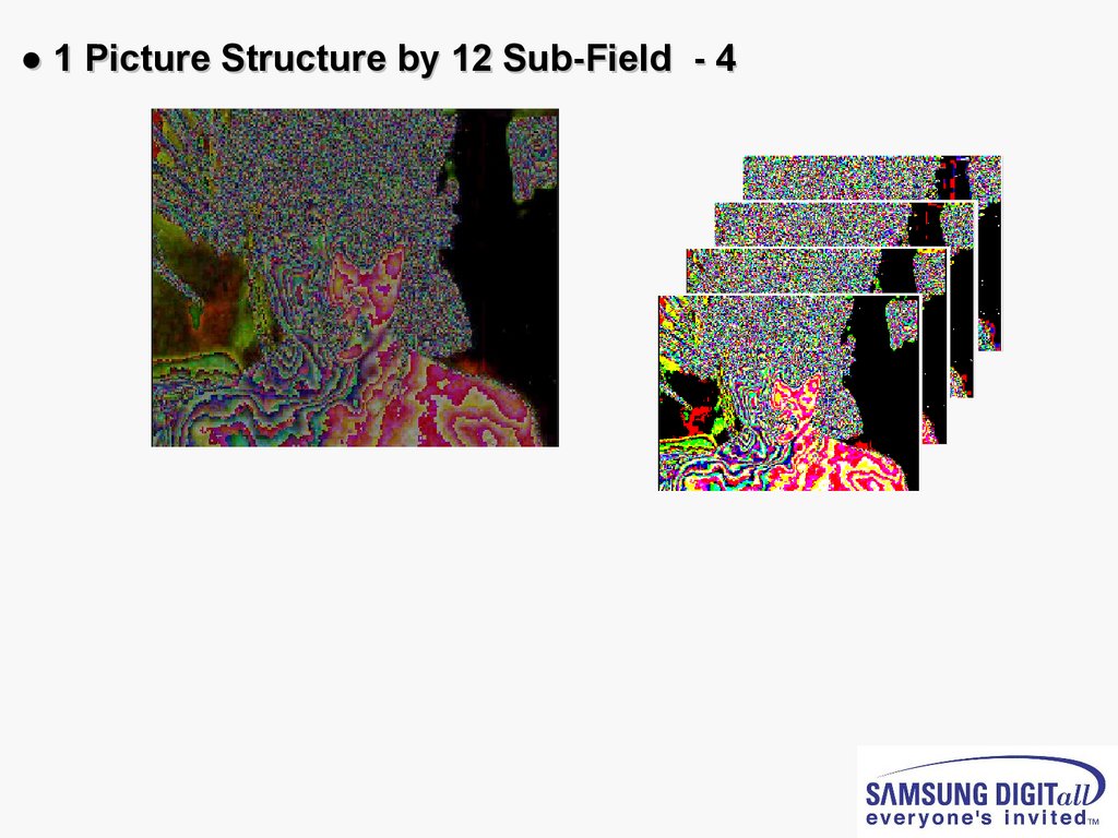
● 1 Picture Structure by 12 Sub-Field - 428.
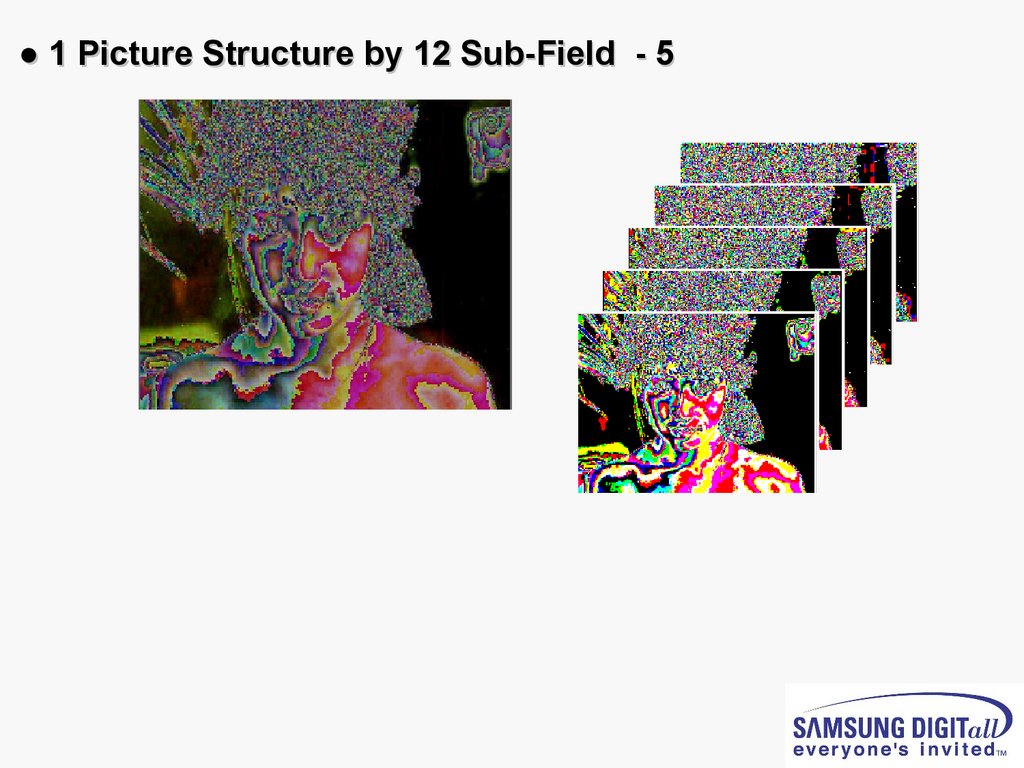
● 1 Picture Structure by 12 Sub-Field - 529.
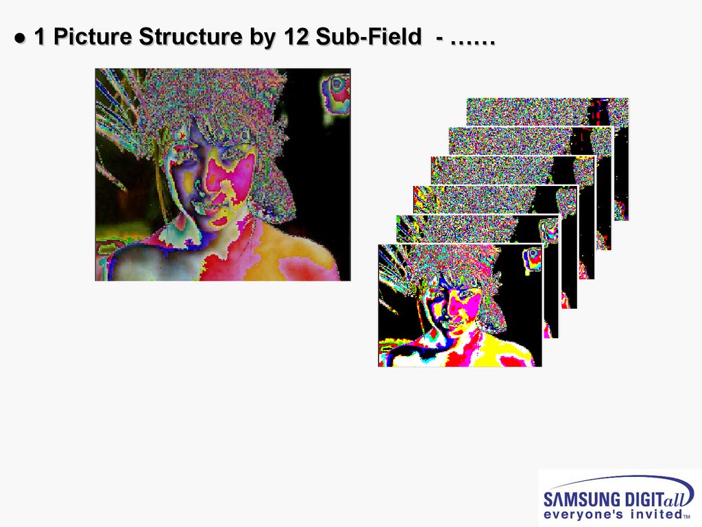
● 1 Picture Structure by 12 Sub-Field - ……30.
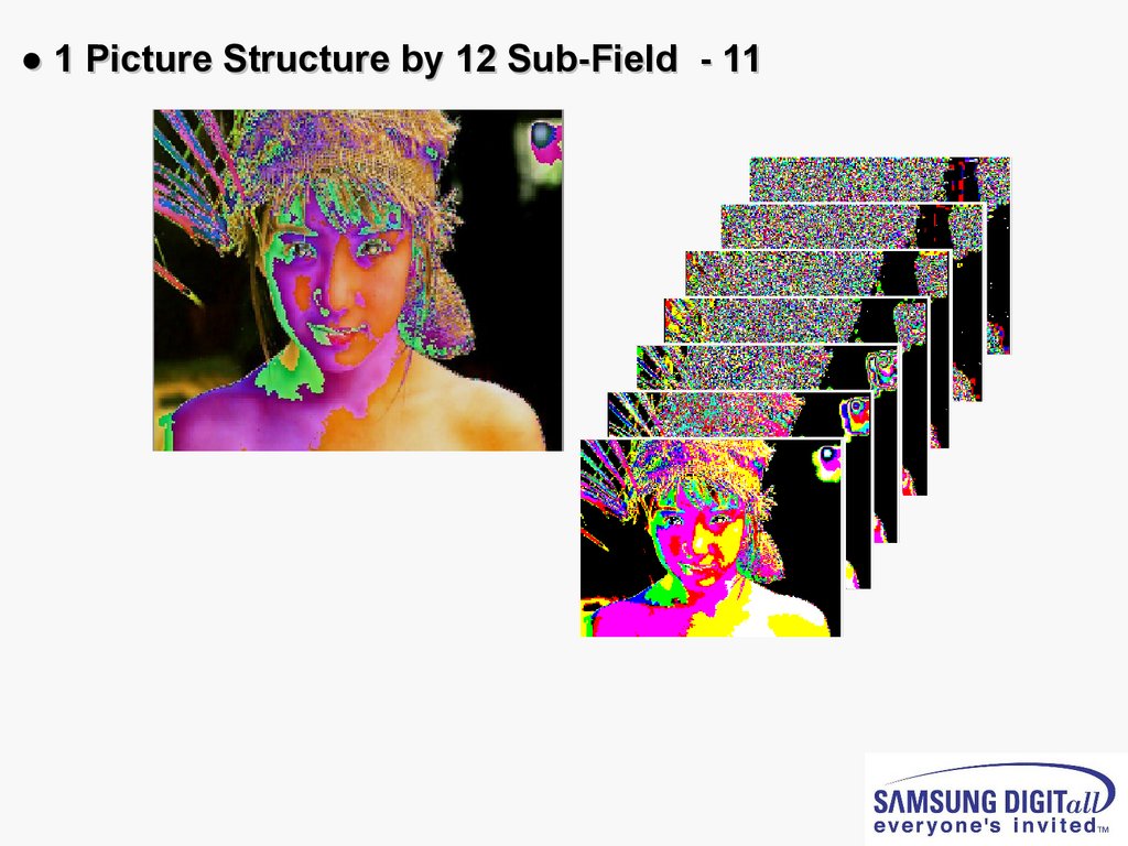
● 1 Picture Structure by 12 Sub-Field - 1131.
● 1 Picture Structure by 12 Sub-Field - 1232.
3. CARNELIAN Training33.
● Comparison with other ModelsProject
LILY2 (W2A)
CARNELIAN (W3)
Brightness
1500cd/m2
1500cd/m2
Contrast ratio
10000:1
15000:1
Tuner
1 Nim Tuner
1 Nim Tuner (Slim)
Audio out
10W x 2
10W x 2
Sound
SRS Tru Surround XT
SRS Tru Surround XT
Speaker
Included
Included
Video input
-
1Side
S-Video input
-
1Side
Component
Input
1Rear
1Rear
Side Input
-
CVBS,S-Video, Headphone
HDMI
1Rear
2Rear
Power
Consumption
42” : 350W
50” : 450W
42” : 380W
50” : 480W
Etc.
-
-
Design
34.
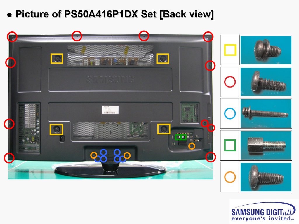
● Picture of PS50A416P1DX Set [Back view]35.
● Picture of CARNELIAN 50” W3 PDP Module [Back view]36.
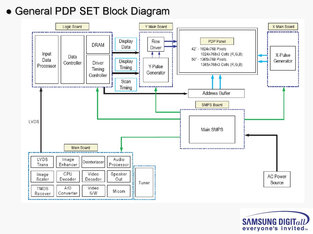
● General PDP SET Block Diagram37.
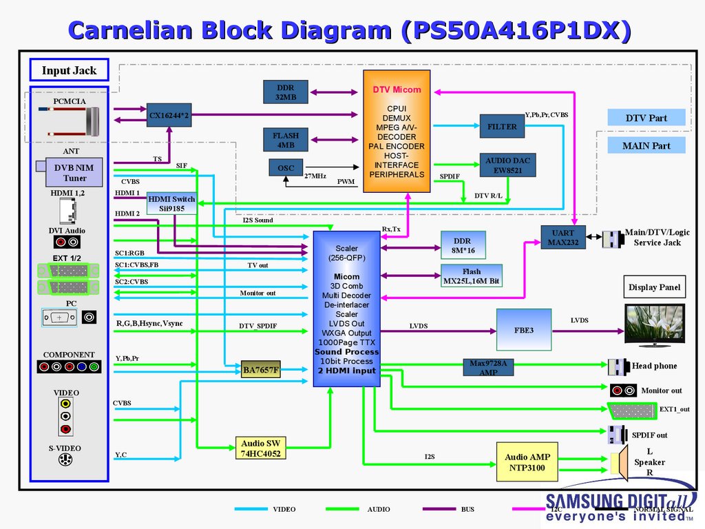
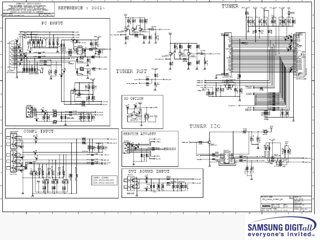
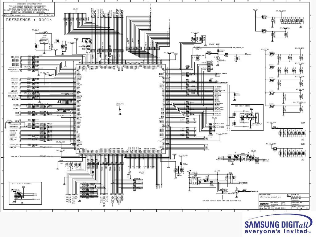
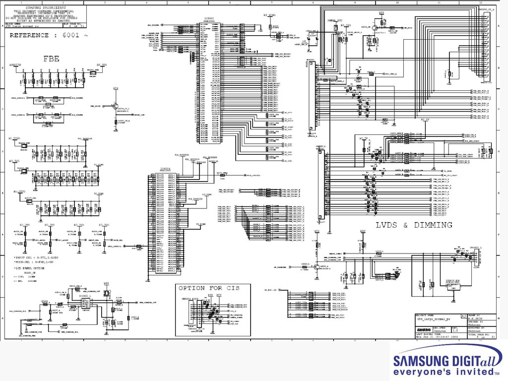
Carnelian Block Diagram (PS50A416P1DX)Input Jack
DDR
32MB
DTV Micom
FLASH
4MB
CPUI
DEMUX
MPEG A/VDECODER
PAL ENCODER
HOSTINTERFACE
PERIPHERALS
PCMCIA
CX16244*2
ANT
DVB NIM
Tuner
HDMI 1,2
TS
SIF
OSC
CVBS
HDMI 1
HDMI 2
27MHz
PWM
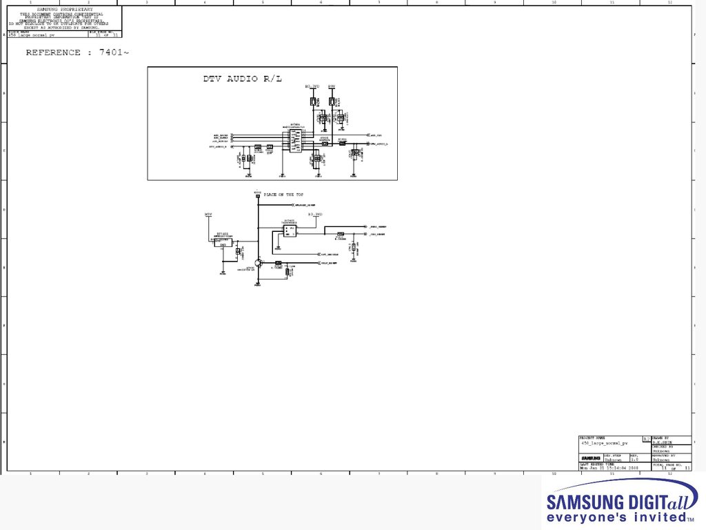
SPDIF
DTV R/L
I2S Sound
TV out
Monitor out
PC
R,G,B,Hsync,Vsync
DTV_SPDIF
Y,Pb,Pr
BA7657F
UART
MAX232
DDR
8M*16
Scaler
(256-QFP)
SC1:RGB
SC2:CVBS
COMPONENT
MAIN Part
AUDIO DAC
EW8521
Rx,Tx
SC1:CVBS,FB
Micom
3D Comb
Multi Decoder
De-interlacer
Scaler
LVDS Out
WXGA Output
1000Page TTX
Sound Process
10bit Process
2 HDMI input
Flash
MX25L,16M Bit
Main/DTV/Logic
Service Jack
Display Panel
LVDS
LVDS
FBE3
Max9728A
AMP
Head phone
Monitor out
VIDEO
CVBS
S-VIDEO
DTV Part
FILTER
HDMI Switch
Sii9185
DVI Audio
EXT 1/2
Y,Pb,Pr,CVBS
Y,C
EXT1_out
SPDIF out
Audio SW
74HC4052
VIDEO
AUDIO
L
Speaker
R
Audio AMP
NTP3100
I2S
BUS
I2C
37
NORMAL SIGNAL
38.
● Picture of PS50A416P1DX Chassis - TopLVDS
3.DTV
Micom
6.DRAM
2.FBE3
7.Sound AMP
5.DDR
1.Scaler
4.HDMI
switch
39.
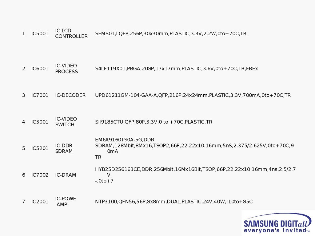
1IC5001
IC-LCD
CONTROLLER
SEMS01,LQFP,256P,30x30mm,PLASTIC,3.3V,2.2W,0to+70C,TR
2
IC6001
IC-VIDEO
PROCESS
S4LF119X01,PBGA,208P,17x17mm,PLASTIC,3.6V,0to+70C,TR,FBEx
3
IC7001
IC-DECODER
UPD61211GM-104-GAA-A,QFP,216P,24x24mm,PLASTIC,3.3V,700mA,0to+70C,TR
4
IC3001
IC-VIDEO
SWITCH
SiI9185CTU,QFP,80P,3.3V,0 to +70C,PLASTIC,TR
IC-DDR
SDRAM
EM6A9160TS0A-5G,DDR
SDRAM,128Mbit,8Mx16,TSOP2,66P,22.22x10.16mm,5nS,2.375/2.625V,0to+70C,9
0mA
TR
5
IC5201
6
IC7002
IC-DRAM
HYB25D256163CE,DDR,256Mbit,16Mx16Bit,TSOP,66P,22.22x10.16mm,4ns,2.5/2.7
V,
-,0to+7
7
IC2001
IC-POWE
AMP
NTP3100,QFN56,56P,8x8mm,DUAL,PLASTIC,24V,40W,-10to+85C
40.
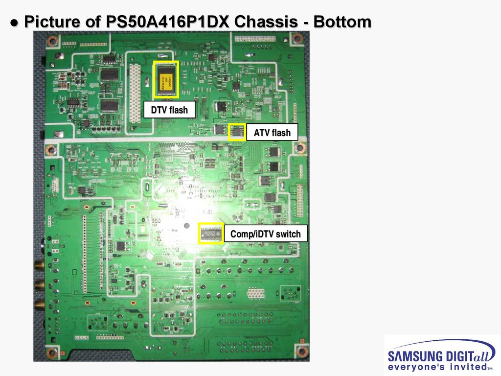
● Picture of PS50A416P1DX Chassis - BottomDTV flash
ATV flash
Comp/iDTV switch
41.
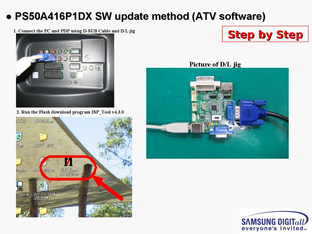
● PS50A416P1DX SW update method (ATV software)1. Connect the PC and PDP using D-SUB Cable and D/L jig
Step by Step
Picture of D/L jig
D-SUB Cable
2. Run the Flash download program ISP_Tool v4.3.0
42.
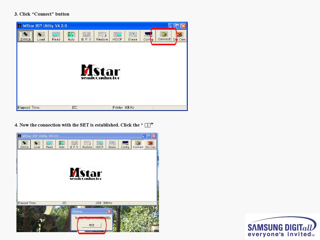
3. Click “Connect” button4. Now the connection with the SET is established. Click the “ 확인”
43.
5. Connect the Power cord and click “Read”①
②
6. Click the new “Read” button
44.
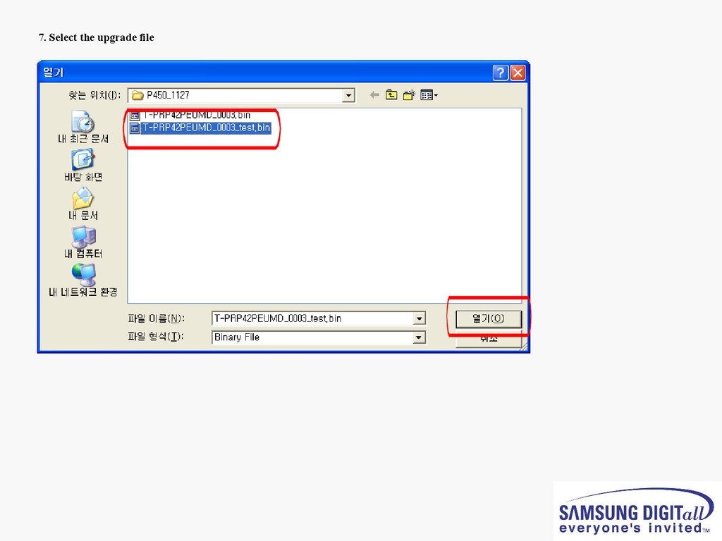
7. Select the upgrade file45.
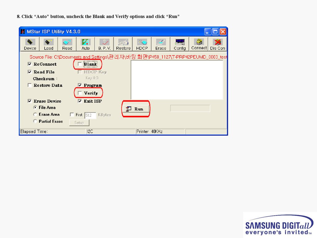
8. Click “Auto” button, uncheck the Blank and Verify options and click “Run”①
46.
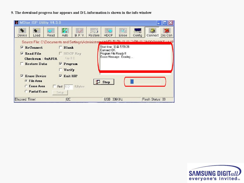
9. The download progress bar appears and D/L information is shown in the info window47.
PS50A416P1DX SW update method (DTV software)Step by Step
1. Connect the serial D/L cable to the SET and execute the D/L program
2. Click the “Browse…” button to select the upgrade file and click “Next
>”
3. Select the appropriate COM port and click “Next >”
4. After a short port scan the communication should be established
Click “Next >” to continue
5. Click “Next >” to continue
48.
PS50A416P1DX SW update method (DTV software)6. The upgrade file is transferring to the SET
You can check the transfer progress bar and the remaining time
8. Wait the upgrade process to finish
You can check the upgrade progress bar
7. After the file was transferred the upgrade process will start
automatically
9. After a successful upgrade the following window appears
Click “OK” to close the program
49.
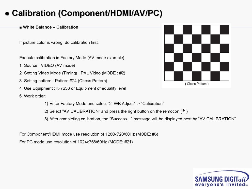
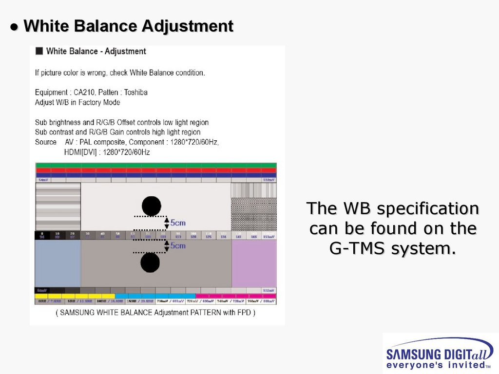
● Calibration (Component/HDMI/AV/PC)■ White Balance – Calibration
If picture color is wrong, do calibration first.
Execute calibration in Factory Mode (AV mode example):
1. Source : VIDEO (AV mode)
2. Setting Video Mode (Timing) : PAL Video (MODE : #2)
3. Setting pattern : Pattern #24 (Chess Pattern)
4. Use Equipment : K-7256 or Equipment of equality level
5. Work order:
1) Enter Factory Mode and select “2. WB Adjust“ -> “Calibration”
2) Select "AV CALIBRATION" and press the right button on the remocon (
)
3) After completing calibration, the “Success…” message will be displayed next by “AV CALIBRATION”
For Component/HDMI mode use resolution of 1280x720/60Hz (MODE: #6)
For PC mode use resolution of 1024x768/60Hz (MODE: #21)
50.
● White Balance AdjustmentThe WB specification
can be found on the
G-TMS system.
51.
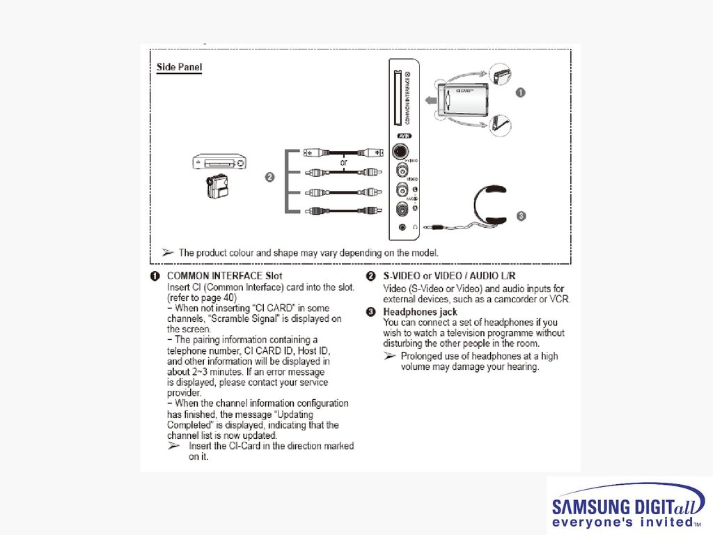
● Picture condition in Factory mode / during WB adjust● Factory mode OSD
52.
53.
54.
55.
56.
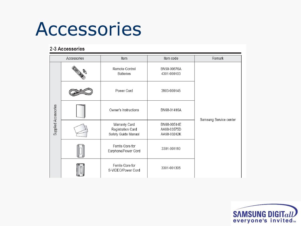
Accessories57.
5. Trouble shooting58.
● Check List in advance■. Each cable connection condition check
- Cable is connected correctly ?
■.Check Voltage
- SMPS Video main Board, SMPS X,Y Drive board, SMPS Logic board
■. The chart below shows abnormal condition
59.
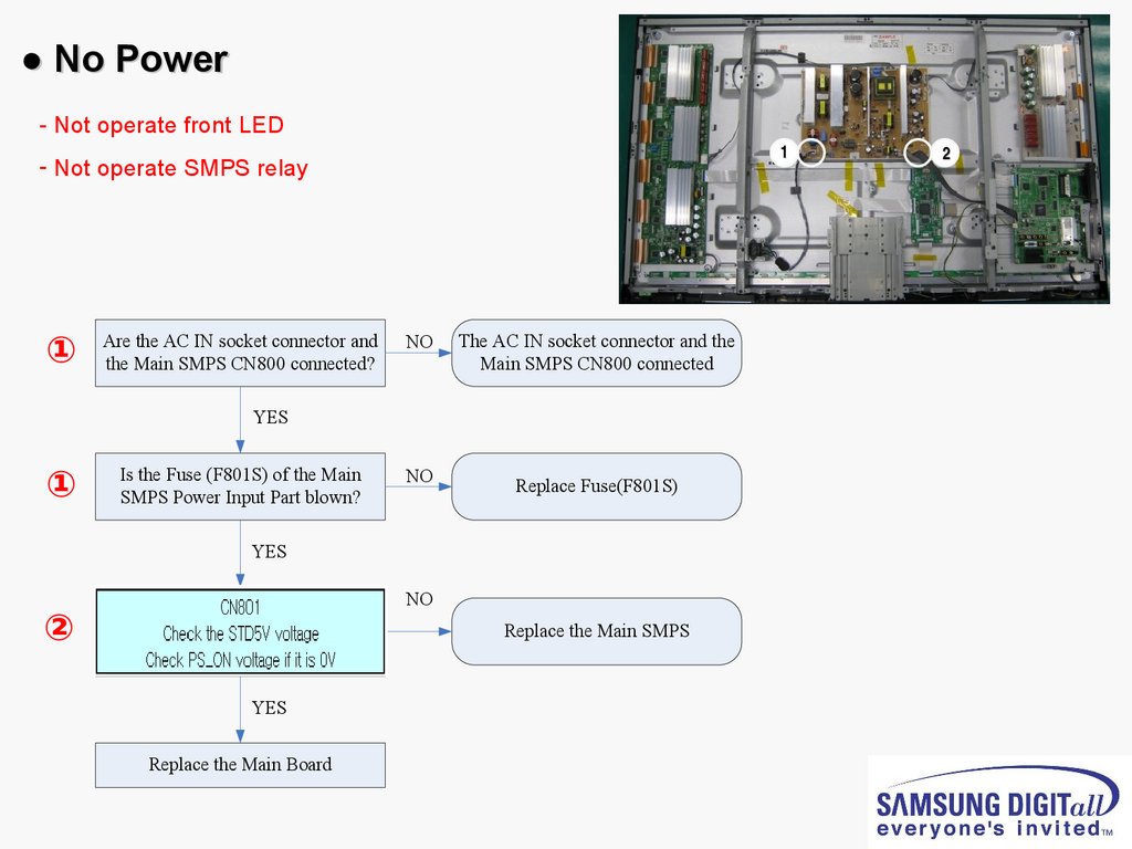
● No Power- Not operate front LED
1
- Not operate SMPS relay
①
Are the AC IN socket connector and
the Main SMPS CN800 connected?
NO
The AC IN socket connector and the
Main SMPS CN800 connected
YES
①
Is the Fuse (F801S) of the Main
SMPS Power Input Part blown?
NO
Replace Fuse(F801S)
YES
②
Main SMPS CN804-1
Pin 3:STB 5V
Pin 8 PS-ON: Check to see If
it is 0V
YES
Replace the Main Board
NO
Replace the Main SMPS
2
60.
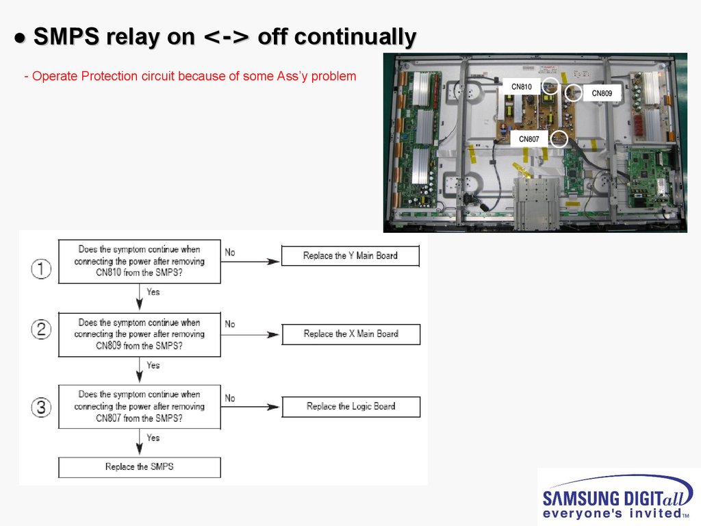
● SMPS relay on <-> off continually- Operate Protection circuit because of some Ass’y problem
CN810
CN807
CN809
61.
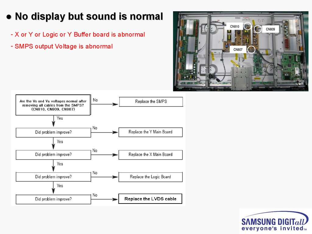
● No display but sound is normalCN810
- X or Y or Logic or Y Buffer board is abnormal
- SMPS output Voltage is abnormal
CN807
CN809
62.
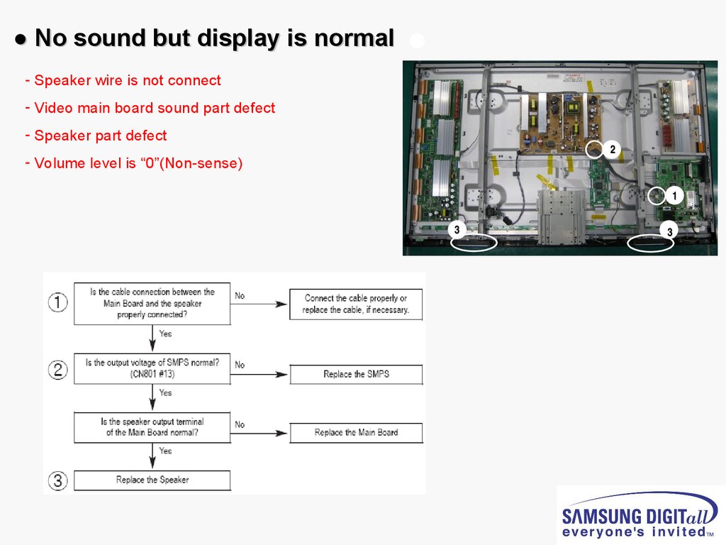
● No sound but display is normal- Speaker wire is not connect
- Video main board sound part defect
- Speaker part defect
2
- Volume level is “0”(Non-sense)
1
3
3
63.
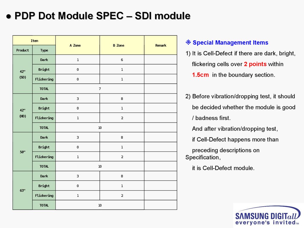
● PDP Dot Module SPEC – SDI moduleItem
A Zone
Product
42"
(SD)
Type
(HD)
Remark
※ Special Management Items
1) It is Cell-Defect if there are dark, bright,
Dark
1
6
Bright
0
1
Flickering
0
1
TOTAL
42"
B Zone
flickering cells over 2 points within
1.5cm in the boundary section.
7
Dark
3
8
2) Before vibration/dropping test, it should
Bright
0
1
be decided whether the module is good
Flickering
1
2
/ badness first.
TOTAL
And after vibration/dropping test,
10
Dark
3
8
Bright
0
1
Flickering
1
2
50"
TOTAL
10
3
8
Bright
0
1
Flickering
1
2
63"
10
preceding descriptions on
Specification,
it is Cell-Defect module.
Dark
TOTAL
if Cell-Defect happens more than
64.
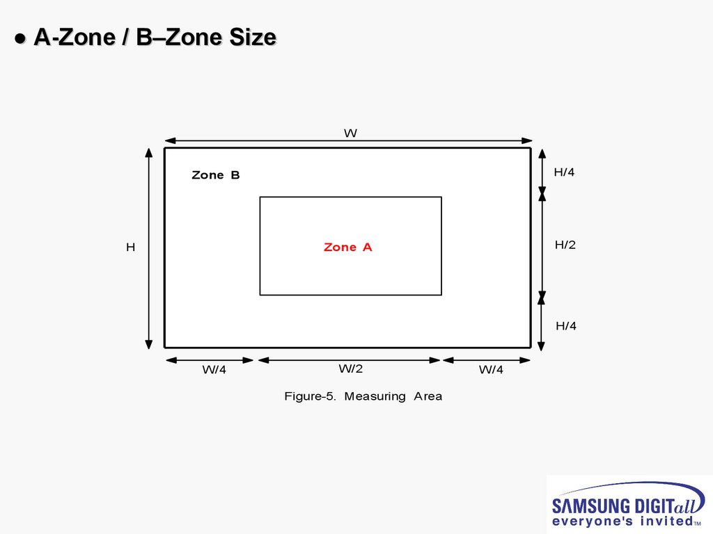
● A-Zone / B–Zone SizeW
H/4
Zone B
H
H/2
Zone A
H/4
W/4
W/2
Figure-5. Measuring Area
W/4