


-(4х2) surface")
-(42) with adsorbed Cs in S4 and S5")
 mathematics
Similar presentations:


")

")

")

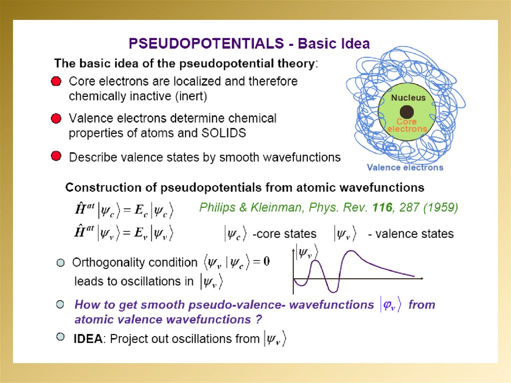
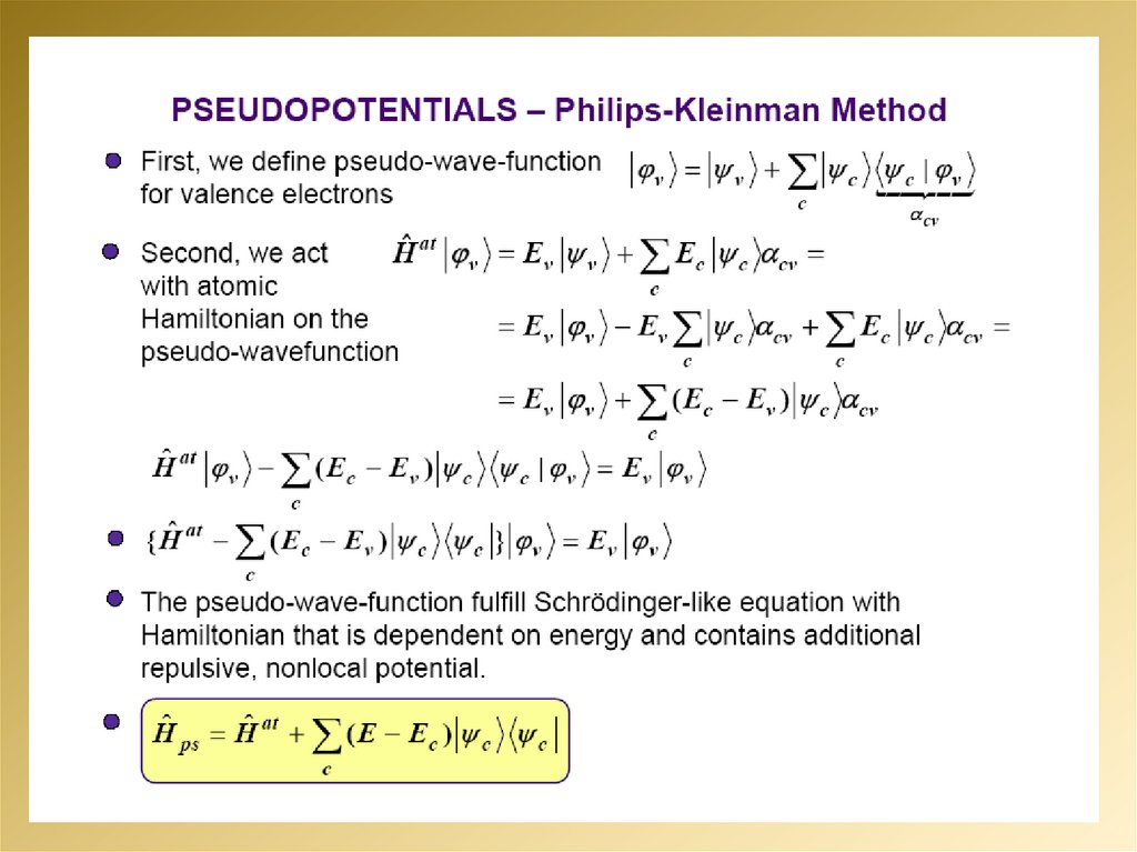
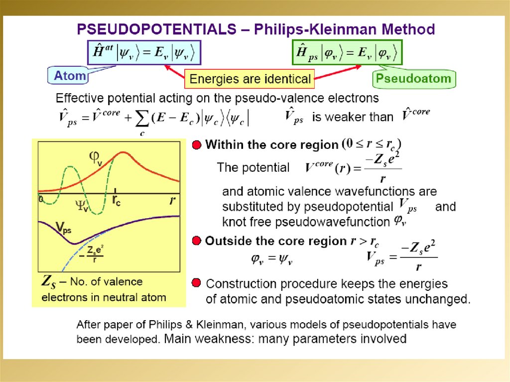
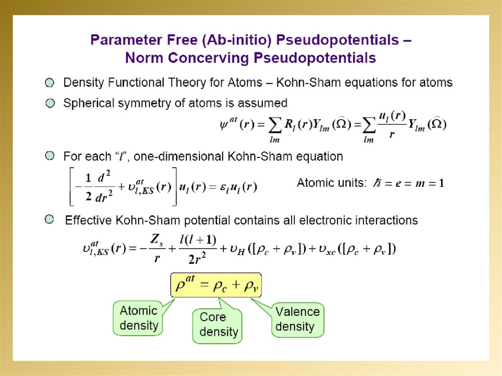
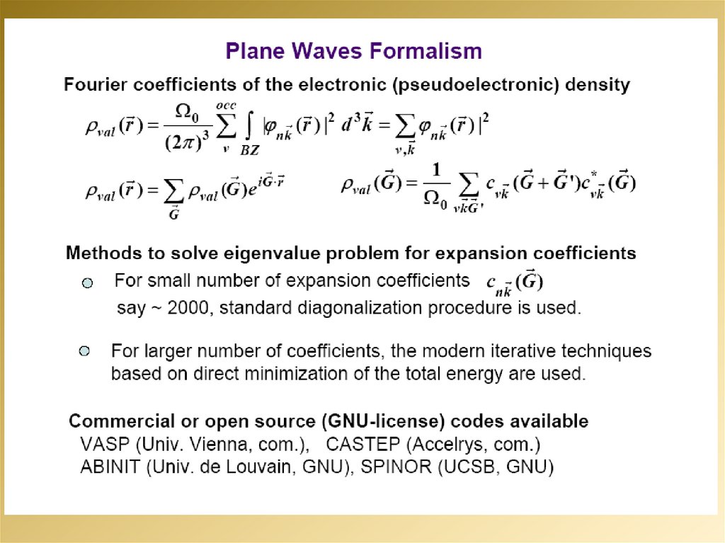
Practical application of the method of Kona-Shema. Pseudopotentials method
1. Лекция 12
Практическое применениеметода Кона-Шема
Метод псевдопотенциалов
2.
3.
4.
5.
6.
7.
Выводы8.
9.
10.
11.
12.
13.
14.
15.
16.
17.
18.
19.
20.
21.
22.
23.
24.
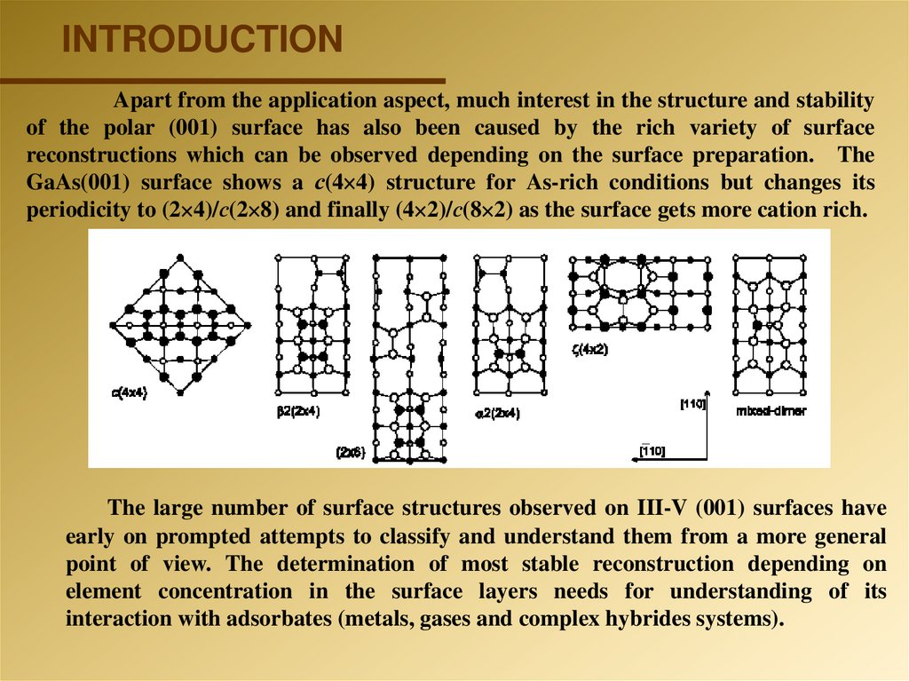
INTRODUCTIONApart from the application aspect, much interest in the structure and stability
of the polar (001) surface has also been caused by the rich variety of surface
reconstructions which can be observed depending on the surface preparation. The
GaAs(001) surface shows a с(4 4) structure for As-rich conditions but changes its
periodicity to (2 4)/с(2 8) and finally (4 2)/с(8 2) as the surface gets more cation rich.
The large number of surface structures observed on III-V (001) surfaces have
early on prompted attempts to classify and understand them from a more general
point of view. The determination of most stable reconstruction depending on
element concentration in the surface layers needs for understanding of its
interaction with adsorbates (metals, gases and complex hybrides systems).
25.
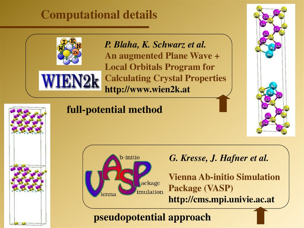
Computational detailsP. Blaha, K. Schwarz et al.
An augmented Plane Wave +
Local Orbitals Program for
Calculating Crystal Properties
http://www.wien2k.at
full-potential method
G. Kresse, J. Hafner et al.
Vienna Ab-initio Simulation
Package (VASP)
http://cms.mpi.univie.ac.at
pseudopotential approach
26.
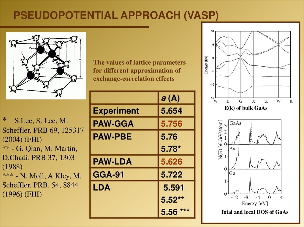
PSEUDOPOTENTIAL APPROACH (VASP)10
The values of lattice parameters
for different approximation of
exchange-correlation effects
Energy [Ev]
5
0
-5
-10
* - S.Lee, S. Lee, M.
Scheffler. PRB 69, 125317
(2004) (FHI)
** - G. Qian, M. Martin,
D.Chadi. PRB 37, 1303
(1988)
*** - N. Moll, A.Kley, M.
Scheffler. PRB. 54, 8844
(1996) (FHI)
Experiment
5.654
PAW-GGA
5.756
PAW-PBE
5.76
5.78*
PAW-LDA
5.626
GGA-91
5.722
LDA
5.591
5.52**
5.56 ***
-15
W
L
G
X
Z
W
E(k) of bulk GaAs
N(E) [el./eV/atom]
a (A)
3 GaAs
2
1
0
As
1
0
Ga
1
0
-12
-8 -4
0
Energy [eV]
4
Total and local DOS of GaAs
K
27. Models of Ga-terminated GaAs(001)-(4х2) surface
GaAs(001) (4x2)GaAs(001) 2(4x2)
GaAs(001) (4x2)
GaAs(001) (4x2)
28.
ELECTRONIC STRUCTURE-
2
a)
b)
Ga-terminated
c)
2
As-terminated
d)
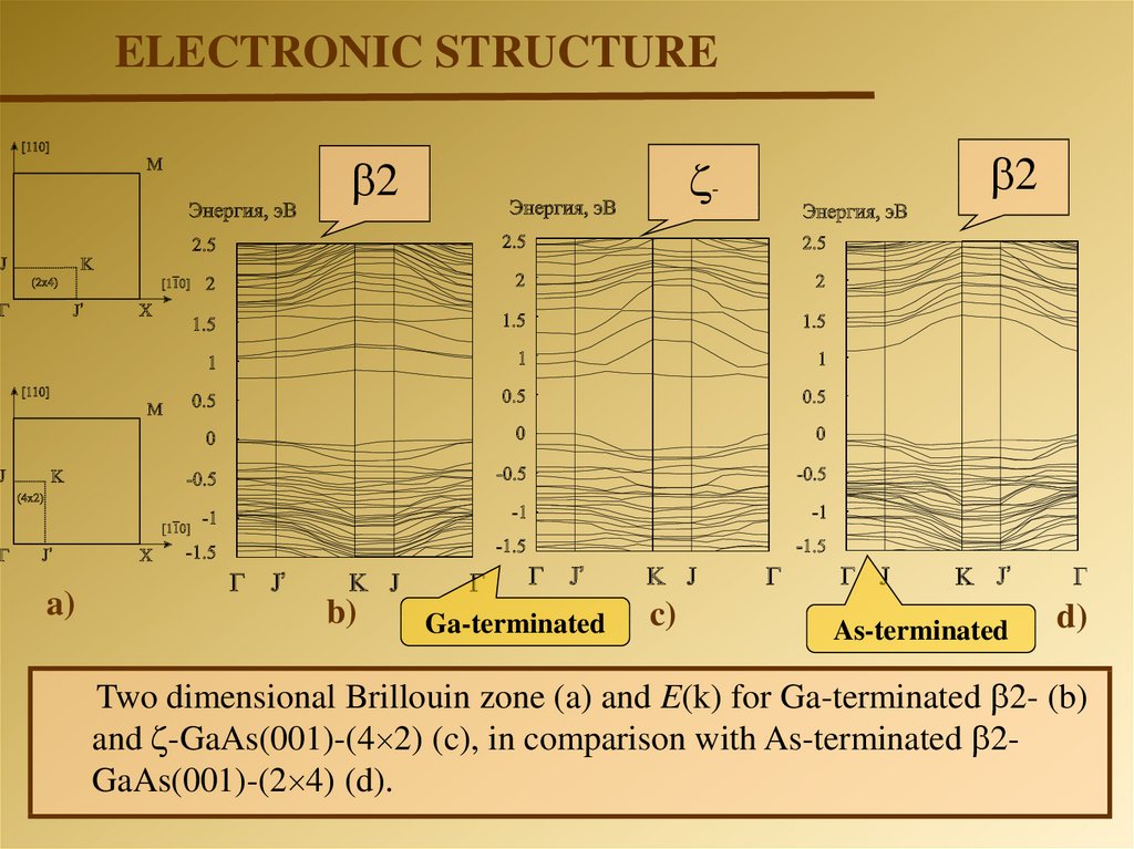
Two dimensional Brillouin zone (a) and E(k) for Ga-terminated 2- (b)
and -GaAs(001)-(4 2) (c), in comparison with As-terminated 2GaAs(001)-(2 4) (d).
29.
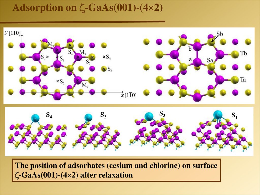
Adsorption on -GaAs(001)-(4 2)-GaAs(001)-(4 2)
S4
S2
S3
The position of adsorbates (cesium and chlorine) on surface
-GaAs(001)-(4 2) after relaxation
S1
30.
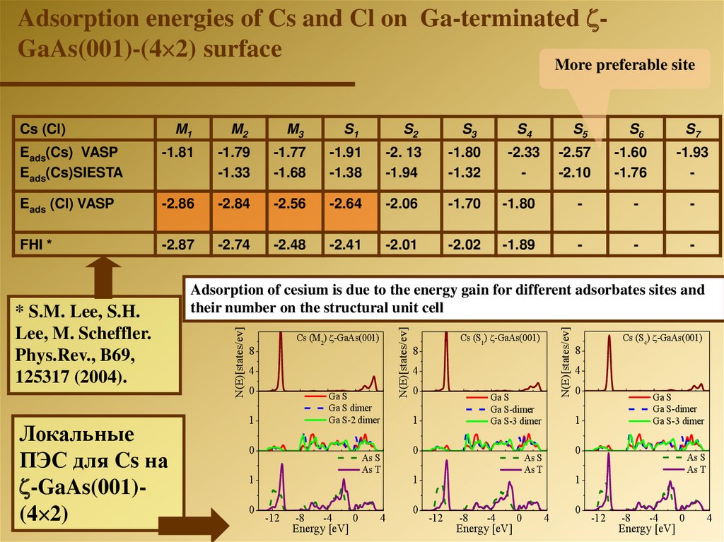
Adsorption energies of Cs and Cl on Ga-terminated GaAs(001)-(4 2) surfaceMore preferable site
M1
M2
M3
S1
S2
Eads(Cs) VASP
Eads(Cs)SIESTA
-1.81
-1.79
-1.33
-1.77
-1.68
-1.91
-1.38
-2. 13
-1.94
-1.80
-1.32
Eads (Cl) VASP
-2.86
-2.84
-2.56
-2.64
-2.06
-1.70
-1.80
-
-
-
FHI *
-2.87
-2.74
-2.48
-2.41
-2.01
-2.02
-1.89
-
-
-
Локальные
ПЭС для Cs на
-GaAs(001)(4 2)
S4
-2.33
-
S5
S6
-2.57
-2.10
-1.60
-1.76
Cs (M2) -GaAs(001)
8
4
0
Ga S
Ga S dimer
Ga S-2 dimer
1
0
1
0
-12
-8
-4
Energy [eV]
0
Cs (S1) -GaAs(001)
8
4
0
Ga S
Ga S-dimer
Ga S-3 dimer
1
As S
As T
4
N(E)[states/ev]
N(E)[states/ev]
* S.M. Lee, S.H.
Lee, M. Scheffler.
Phys.Rev., B69,
125317 (2004).
S3
S7
-1.93
-
Adsorption of cesium is due to the energy gain for different adsorbates sites and
their number on the structural unit cell
N(E)[states/ev]
Cs (Cl)
0
0
-12
-8
-4
Energy [eV]
0
8
4
0
Ga S
Ga S-dimer
Ga S-3 dimer
1
0
As S
As T
1
Cs (S4) -GaAs(001)
As S
As T
1
4
0
-12
-8
-4
Energy [eV]
0
4
31.
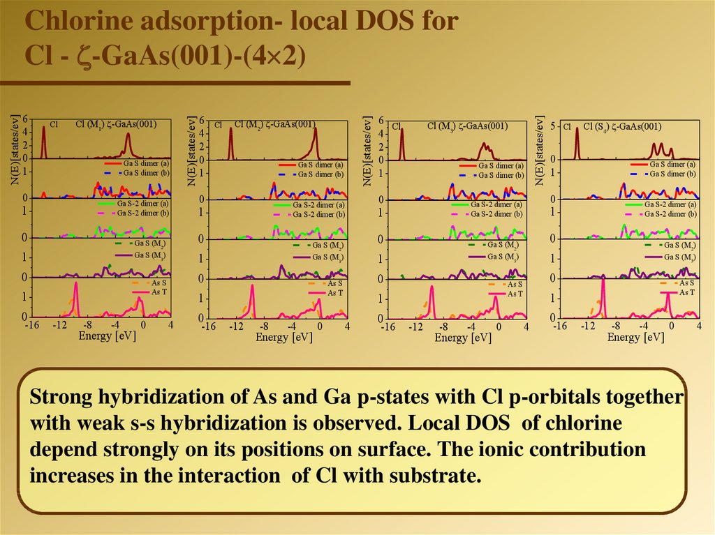
Cl (М1) -GaAs(001)Ga S dimer (a)
Ga S dimer (b)
0
Ga S-2 dimer (a)
Ga S-2 dimer (b)
1
0
0
0
-16
-12
-8
-4
Energy [eV]
0
Cl (M2) -GaAs(001)
Ga S dimer (a)
Ga S dimer (b)
0
Ga S-2 dimer (a)
Ga S-2 dimer (b)
1
0
4
0
-16
-12
-8
-4
Energy [eV]
0
Cl (M3) -GaAs(001)
Ga S dimer (a)
Ga S dimer (b)
0
4
0
-16
-12
-8
-4
Energy [eV]
0
Cl (S4) -GaAs(001)
0
1
Ga S dimer (a)
Ga S dimer (b)
Ga S-2 dimer (a)
Ga S-2 dimer (b)
0
Ga S (M2)
Ga S (M3)
1
0
As S
As T
1
Cl
1
Ga S (M2)
Ga S (M3)
0
5
0
Ga S-2 dimer (a)
Ga S-2 dimer (b)
1
1
As S
As T
1
6 Cl
4
2
0
1
0
Ga S (M2)
Ga S (M3)
1
As S
As T
1
Cl
0
Ga S (M2)
Ga S (M3)
1
6
4
2
0
1
N(E)[states/ev]
Cl
N(E)[states/ev]
6
4
2
0
1
N(E)[states/ev]
N(E)[states/ev]
Chlorine adsorption- local DOS for
Cl - -GaAs(001)-(4 2)
As S
As T
1
4
0
-16
-12
-8
-4
Energy [eV]
0
Strong hybridization of As and Ga p-states with Cl p-orbitals together
with weak s-s hybridization is observed. Local DOS of chlorine
depend strongly on its positions on surface. The ionic contribution
increases in the interaction of Cl with substrate.
4
32.
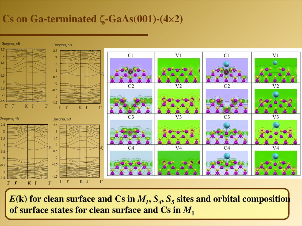
Cs on Ga-terminated -GaAs(001)-(4 2)E(k) for clean surface and Cs in М1, S4, S5 sites and orbital composition
of surface states for clean surface and Cs in М1
33.
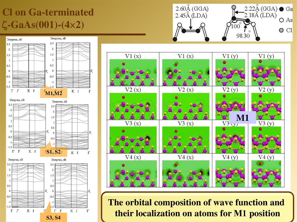
Cl on Ga-terminated-GaAs(001)-(4 2)
М1,М2
M1
S1, S2
S3, S4
The orbital composition of wave function and
their localization on atoms for М1 position
34.
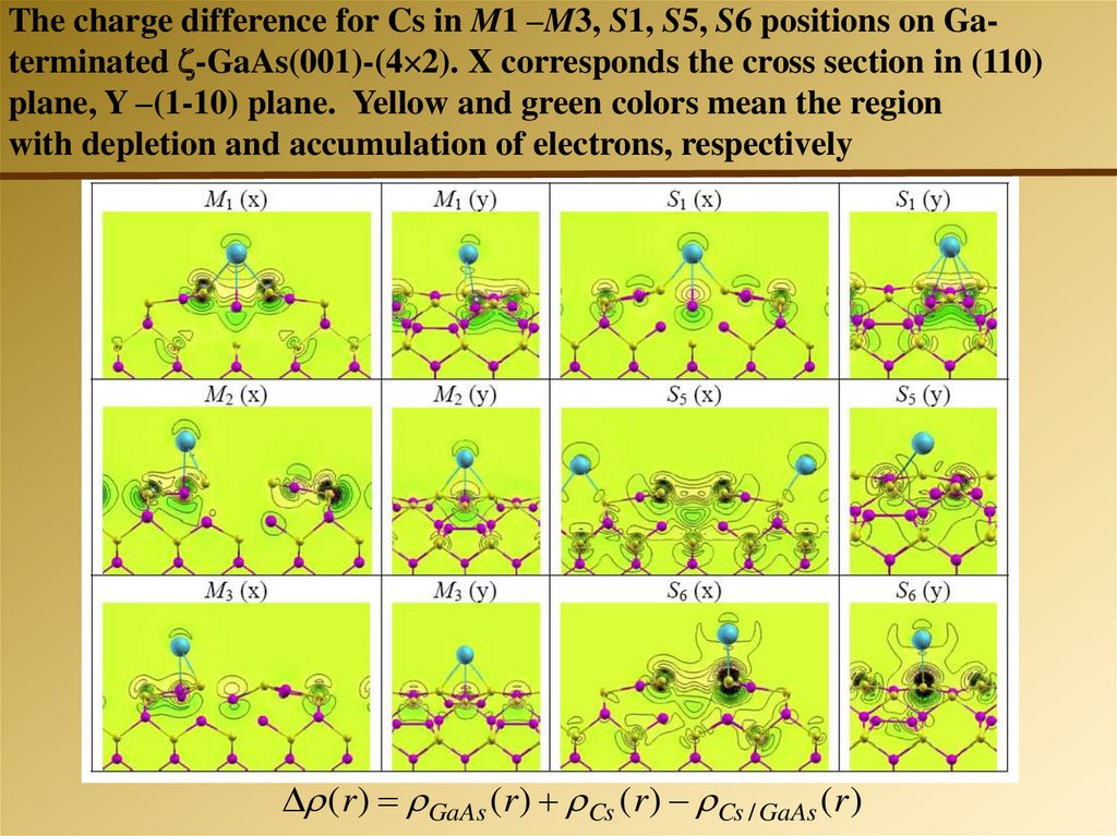
The charge difference for Cs in M1 –M3, S1, S5, S6 positions on Gaterminated -GaAs(001)-(4 2). X corresponds the cross section in (110)plane, Y –(1-10) plane. Yellow and green colors mean the region
with depletion and accumulation of electrons, respectively
( r ) GaAs ( r ) Cs ( r ) Cs / GaAs ( r )
35.
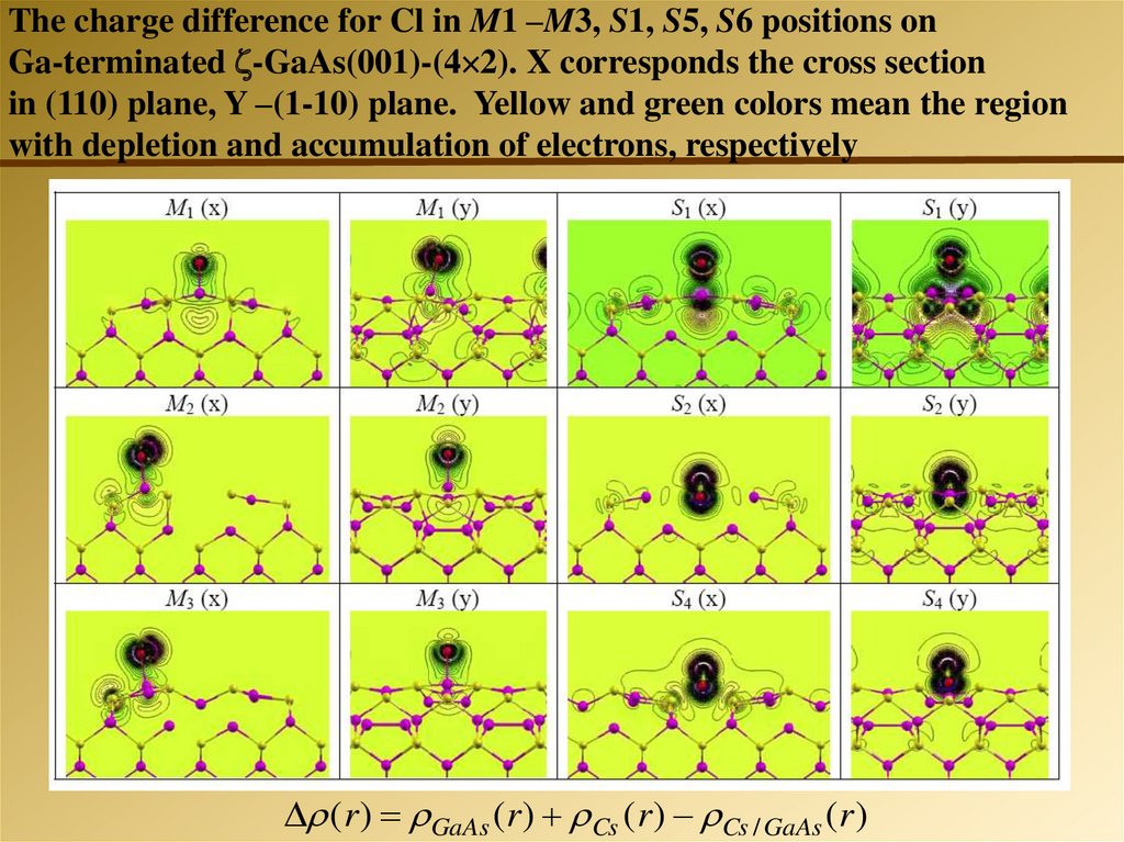
The charge difference for Cl in M1 –M3, S1, S5, S6 positions onGa-terminated -GaAs(001)-(4 2). X corresponds the cross section
in (110) plane, Y –(1-10) plane. Yellow and green colors mean the region
with depletion and accumulation of electrons, respectively
( r ) GaAs ( r ) Cs ( r ) Cs / GaAs ( r )
36.
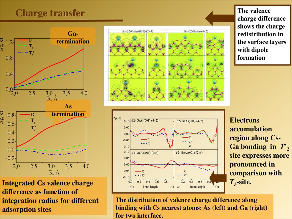
The valencecharge difference
shows the charge
redistribution in
the surface layers
with dipole
formation
, el.
Charge transfer
1,2
0,8
D
T4
T 2'
Gatermination
0,4
, el.
0,0
2,0
0,8
0,6
0,4
0,2
0,0
-0,2
2,0
2,5
D
T3
T2'
3,0 o 3,5
R, A
4,0
As
termination
, el.
0,10 2- GaAs(001)-(4 2)
2- GaAs(001)-(4 2)
0,05
0,00
T4
T2'
D
T4
T2'
-0,05
-0,10
0,10 2- GaAs(001)-(2 4)
2- GaAs(001)-(2 )
0,05
2,5
3,0
3,5
R, A
4,0
Integrated Cs valence charge
difference as function of
integration radius for different
adsorption sites
0,00
-0,05
-0,10
0,0
Cs
T3
T2'
T3
T2'
0,2
0,4
0,6
bond length
0,8
0,2
As Cs
0,4
0,6
bond length
0,8
1,0
Ga
Electrons
accumulation
region along CsGa bonding in Т’2
site expresses more
pronounced in
comparison with
T3-site.
The distribution of valence charge difference along
binding with Cs nearest atoms: As (left) and Ga (right)
for two interface.
37. The adsorption energies of Cs for S1 and S2 sites on -GaAs(001)-(42) with adsorbed Cs in S4 and S5
Cs adsorption on -GaAs(001)-(4 2) (coverage increase)The adsorption energies of Cs for S1 and S2 sites on GaAs(001)-(4 2) with adsorbed Cs in S4 and S5
Cs (S1-S5) -GaAs(001)
12
8
4
0
Ga S
Ga S-dimer
Ga S-2 dimer
0
1
-8
-4
Energy [eV]
0
Ga S
Ga S-dimer
Ga S-2 dimer
0
4
0
S1-S4
S2
S4
S2-S5
As-S
As-Т
1
-12
S2-S4
-1.93
S2
-2.13
S4
-2.33
Cs (S2-S4) -GaAs(001)
1
As-S
As-Т
S1-S4
-1.66
S1
-1.91
S4
-2.33
S1-S5
12
8
4
0
S1
S5
1
0
S2-S5
-1.96
S2
-2.13
S5
-2.57
N(E)[states/ev]
N(E)[states/ev]
S1-S5
-1.71
S1
-1.97
S5
-2.57
-12
-8
-4
0
4
S2-S4
38.
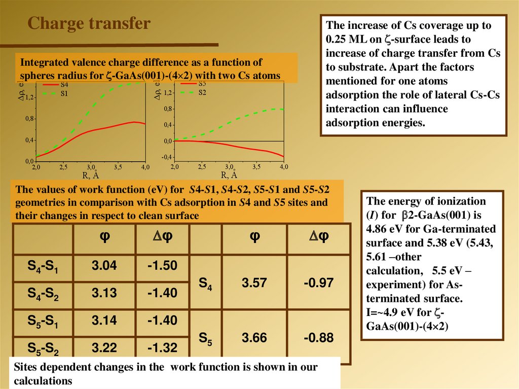
Charge transferThe increase of Cs coverage up to
0.25 ML on -surface leads to
increase of charge transfer from Cs
to substrate. Apart the factors
mentioned for one atoms
adsorption the role of lateral Cs-Cs
interaction can influence
adsorption energies.
1,2
, el.
, el.
Integrated valence charge difference as a function of
spheres radius for -GaAs(001)-(4 2) with two Cs atoms
S4
S1
1,2
S5
S2
0,8
0,8
0,4
0,4
0,0
2,0
0,0
2,5
3,0o
3,5
R, A
4,0
-0,4
2,0
2,5
3,0o
R, A
3,5
4,0
The values of work function (eV) for S4-S1, S4-S2, S5-S1 and S5-S2
geometries in comparison with Cs adsorption in S4 and S5 sites and
their changes in respect to clean surface
φ
φ
S4-S1
3.04
-1.50
S4-S2
3.13
-1.40
S5-S1
3.14
-1.40
S5-S2
3.22
-1.32
φ
φ
S4
3.57
-0.97
S5
3.66
-0.88
Sites dependent changes in the work function is shown in our
calculations
The energy of ionization
(I) for 2-GaAs(001) is
4.86 eV for Ga-terminated
surface and 5.38 eV (5.43,
5.61 –other
calculation, 5.5 eV –
experiment) for Asterminated surface.
I=~4.9 eV for GaAs(001)-(4 2)
39.
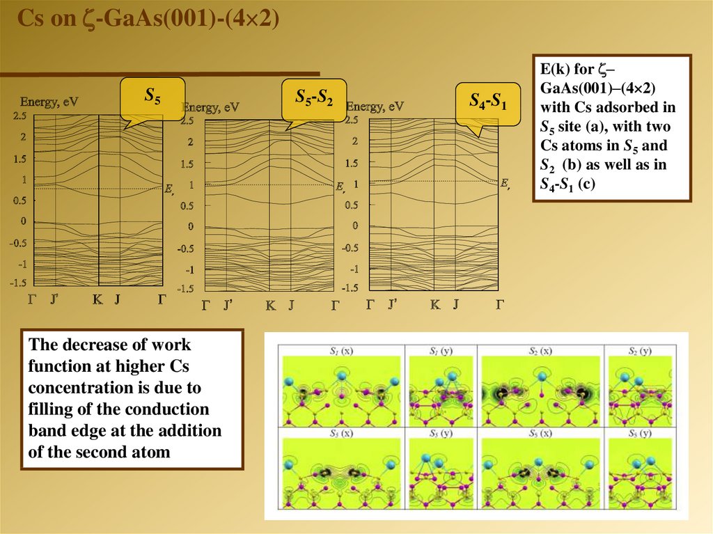
Cs on -GaAs(001)-(4 2)S5
The decrease of work
function at higher Cs
concentration is due to
filling of the conduction
band edge at the addition
of the second atom
S5-S2
S4-S1
E(k) for –
GaAs(001)–(4 2)
with Cs adsorbed in
S5 site (a), with two
Cs atoms in S5 and
S2 (b) as well as in
S4-S1 (c)
40.
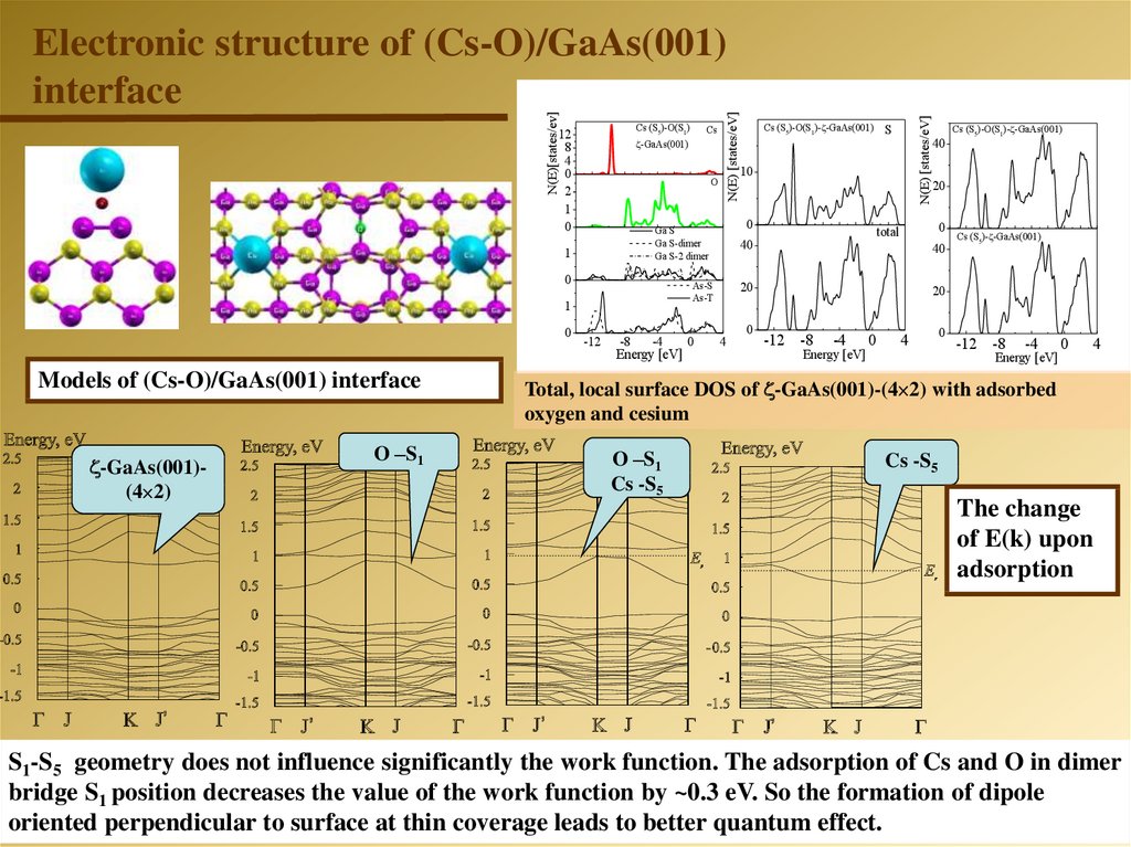
O0
Models of (Cs-O)/GaAs(001) interface
-GaAs(001)(4 2)
O –S1
-12
-8
-4
Energy [eV]
0
S
10
0
Cs (S5)-O(S1)- -GaAs(001)
20
0
40
20
4
40
total
40
As-S
As-Т
1
Cs (S5)-O(S1)- -GaAs(001)
0
Ga S
Ga S-dimer
Ga S-2 dimer
1
0
Cs
-GaAs(001)
N(E) [states/eV]
Cs (S5)-O(S1)
12
8
4
0
2
1
0
N(E) [states/eV]
N(E)[states/ev]
Electronic structure of (Cs-O)/GaAs(001)
interface
Cs (S5)- -GaAs(001)
20
-12 -8
-4
Energy [eV]
0
4
0
-12 -8
-4
Energy [eV]
0
4
Total, local surface DOS of -GaAs(001)-(4 2) with adsorbed
oxygen and cesium
O –S1
Cs -S5
Cs -S5
The change
of E(k) upon
adsorption
S1-S5 geometry does not influence significantly the work function. The adsorption of Cs and O in dimer
bridge S1 position decreases the value of the work function by ~0.3 eV. So the formation of dipole
oriented perpendicular to surface at thin coverage leads to better quantum effect.
41.
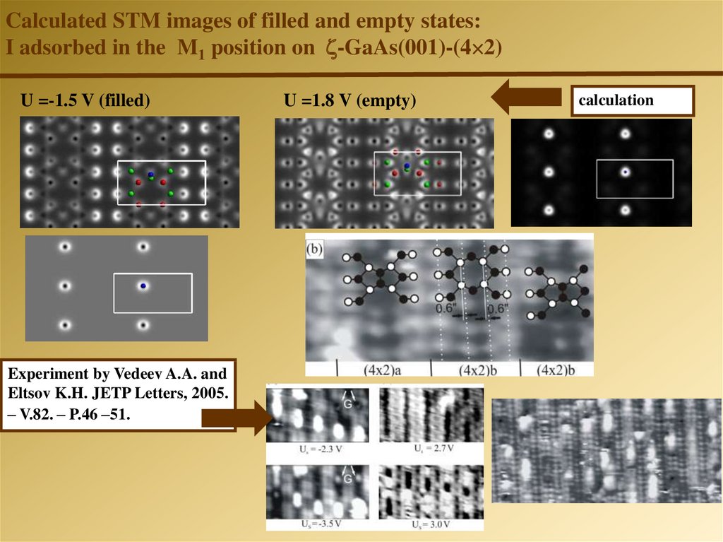
Calculated STM images of filled and empty states:I adsorbed in the M1 position on -GaAs(001)-(4 2)
U =-1.5 V (filled)
Experiment by Vedeev A.A. and
Eltsov K.H. JETP Letters, 2005.
– V.82. – P.46 –51.
U =1.8 V (empty)
calculation
42.
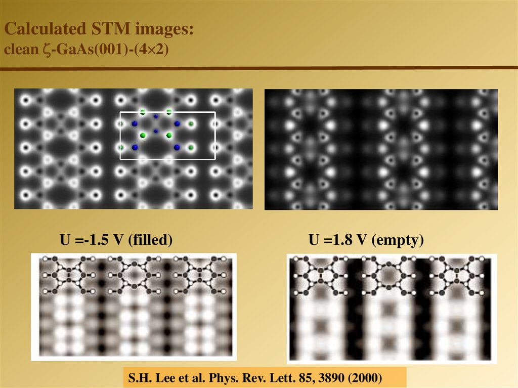
Calculated STM images:clean -GaAs(001)-(4 2)
U =-1.5 V (filled)
U =1.8 V (empty)
S.H. Lee et al. Phys. Rev. Lett. 85, 3890 (2000)
43.
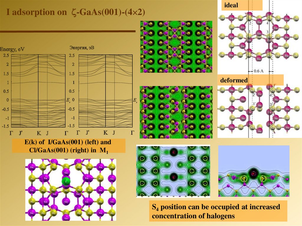
I adsorption on -GaAs(001)-(4 2)ideal
deformed
E(k) of I/GaAs(001) (left) and
Cl/GaAs(001) (right) in M1
S4 position can be occupied at increased
concentration of halogens