Similar presentations:
Cache memory. Lecture №7
1.
Lecture № 7CACHE MEMORY
Continuation
2.
3.
4.
5.
Cache DesignMapping Function (direct, associative, set
associative)
Replacement Algorithm (LRU, FIFO, LFU,
Random)
Write Policy (Information integrity)(Write
through, Write back)
Block Size (no definitive optimum value has
been found)
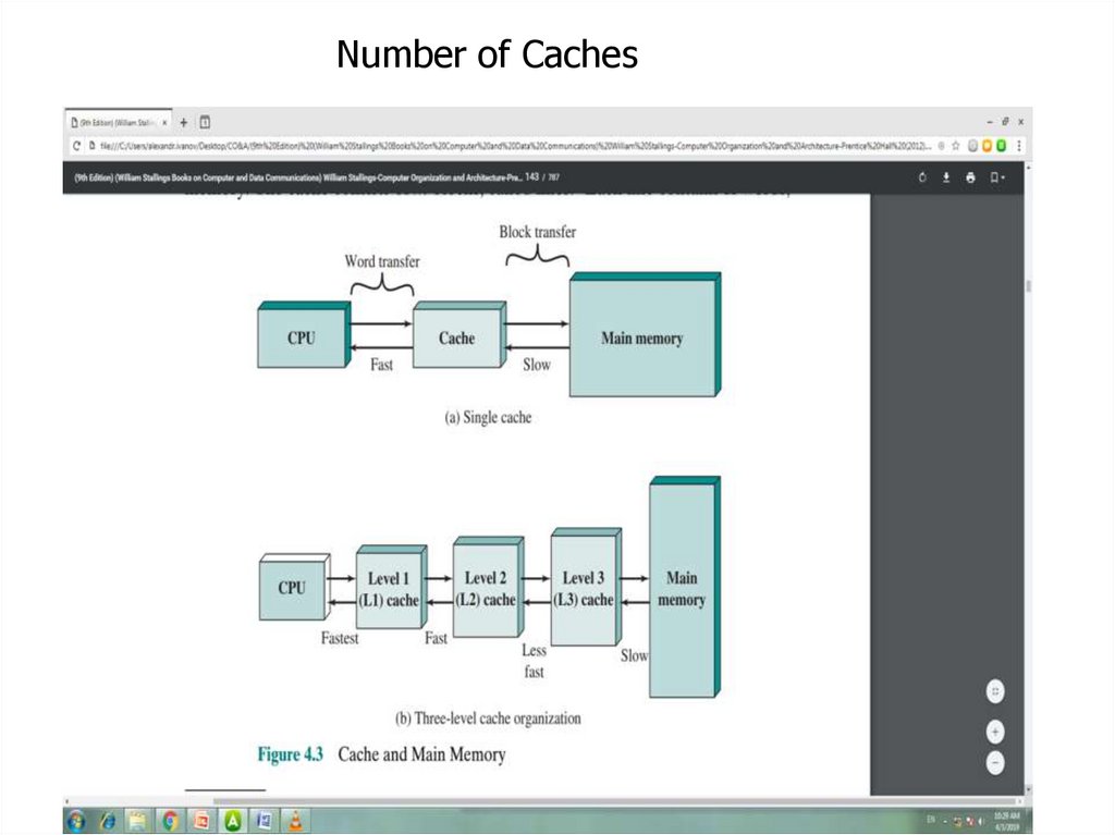
Number of Caches (Single- or two-level,
Unified or Split)
Size (more optimal size: between 1K and 512K)
6.
What’s for are used Cache replacement algorithms?Cache replacement algorithms are used to optimize the time taken by processor
to process the information by storing the information needed by processor at
that time and possibly in future so that if processor needs that information, it can
be provided immediately.
What algorithms are used for cache content replacement?
Traditional cache replacement algorithms include LRU, LFU, Random and some of
their variants. Least Recently Used (LRU) expels the object from the cache that was
asked for the least number of times, of late. Least Frequently Used (LFU) expels the
object that was retrieved least frequently from the cache.
The most efficient caching algorithm would be to always discard the information that will not be needed for the longest time in the future.
This optimal result is referred to as Bélády's optimal algorithm/simply optimal replacement policy or the clairvoyant algorithm.
Самый эффективный алгоритм кэширования - всегда отбрасывать информацию, которая не понадобится в течение долгого времени в будущем. Этот
оптимальный результат называется оптимальным алгоритмом Белади / просто оптимальной политикой замены или алгоритмом ясновидения.
7.
On what property is based effectiveness of cache mechanism?The effectiveness of the cache mechanism is based on a property of
computer programs called locality of reference. Analysis of
programs shows that most of their execution time is spent on
routines in which many instructions are executed repeatedly. These
instructions may constitute a simple loop, nested loops, or a few
procedures that repeatedly call each other.
8.
9.
What’s meant by Cache’s write policy?A cache's write policy is the behavior of a cache while performing a write
operation. A cache's write policy plays a central part in all the variety of
different characteristics exposed by the cache.
What is write-back and write-through caches?
Write-back (or Write-behind): Writing is done only from the cache the
back-end storage. A modified cache block is written back to the store, just
before it is replaced. Write-through: When data is updated, it is written to
both the cache and the back-end storage.
10.
What size is optimal for a cache line?For high performance microprocessor designs, line sizes in the
range 16-64 bytes seem best; shorter line sizes yield high delays due
to memory latency, although they reduce memory traffic somewhat.
How does the cache size affect the hit rates?
The larger the cache, the better the chances are that least recently
accessed information remains in the cache and has not been
automatically removed. The smaller the cache, the more likely that least
recently accessed information will be removed from the cache.
11.
What does unified cache mean?A unified cache is a cache that contains both code (instructions) and data.
The L2 Cache is a unified code/data cache that services requests forwarded to
it from both the L1 Data Cache and the L1 Code Cache.
What does split cache mean?
A split cache is a cache that consists of two physically separate parts, where
one part, called the instruction cache, is dedicated for holding instructions and the
other, called the data cache, is dedicated for holding data (i.e., instruction memory
operands).
12.
Number of Caches13.
14.
15.
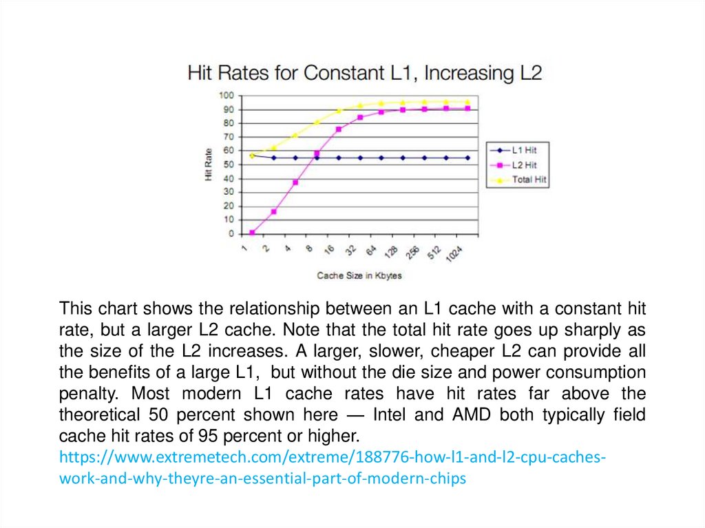
This chart shows the relationship between an L1 cache with a constant hitrate, but a larger L2 cache. Note that the total hit rate goes up sharply as
the size of the L2 increases. A larger, slower, cheaper L2 can provide all
the benefits of a large L1, but without the die size and power consumption
penalty. Most modern L1 cache rates have hit rates far above the
theoretical 50 percent shown here — Intel and AMD both typically field
cache hit rates of 95 percent or higher.
https://www.extremetech.com/extreme/188776-how-l1-and-l2-cpu-cacheswork-and-why-theyre-an-essential-part-of-modern-chips
16.
17.
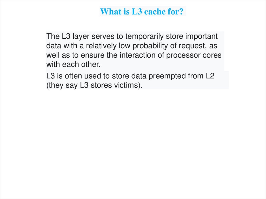
What is L3 cache for?The L3 layer serves to temporarily store important
data with a relatively low probability of request, as
well as to ensure the interaction of processor cores
with each other.
L3 is often used to store data preempted from L2
(they say L3 stores victims).
18.
19.
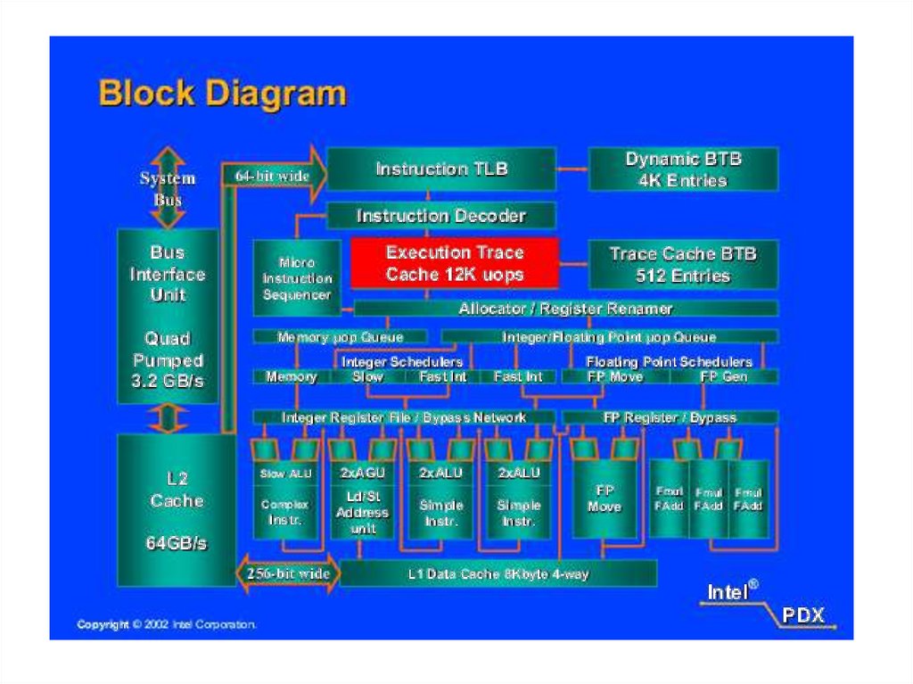
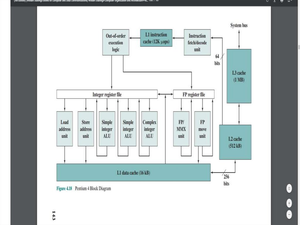
Unlike the organization used in all previous Pentium models, and in most otherprocessors, the Pentium 4 instruction cache sits between the instruction decode logic
and the execution core. The reasoning behind this design decision is as follows: the
Pentium process decodes, or translates, Pentium machine instructions into simple
RISC-like instructions called micro-operations. The use of simple, fixed-length
micro-operations enables the use of superscalar pipelining and scheduling
techniques that enhance performance. However, the Pentium machine instructions
are cumbersome to decode; they have a variable number of bytes and many
different options. It turns out that performance is enhanced if this decoding is done
independently of the scheduling and pipelining logic.
The data cache employs a write-back policy: Data are written to main memory only
when they are removed from the cache and there has been an update. The Pentium 4
processor can be dynamically configured to support write-through caching.
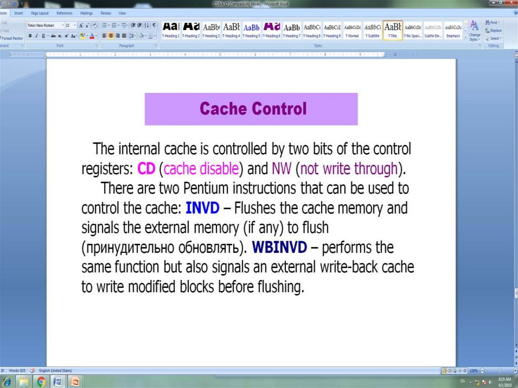
The L1 data cache is controlled by two bits in one of the control registers, labeled
the CD (cache disable) and NW (not write-through) bits. There are also two
Pentium 4 instructions that can be used to control the data cache: INVD invalidates
(flushes) the internal cache memory and signals the external cache (if any) to
invalidate. WBINVD writes back and invalidates internal cache and then writes
back and invalidates external cache. Both the L2 and L3 caches are eight-way setassociative with a line size of 128 bytes.
20.
21.
What do you mean by out of order execution?Out-of-order execution (OoOE) is an approach to processing that
allows instructions for high-performance microprocessors to
begin execution as soon as their operands are ready. Although
instructions are issued in-order, they can proceed out-of- order with
respect to each other.
Managing speculative execution
• Common implementation:
Fetch/Decode instructions from the predicted execution path
Instructions can execute as soon as their operands become ready
• Instructions can graduate and commit to memory only once it is
certain they should have been executed
An instruction commits only when all previous (in-order)
instructions have committed ⇒ instructions commit in-order
Instructions on a mis-predicted execution path are flushed
22.
23.
What is the victim cache ?The victim cache is a hardware cache designed to reduce collision misses
and reduce hit latency for direct-mapped caches. It is used in the way of
replenishing the level 1 cache, so that any cache-line that is removed
from the cache is cached in the victim's cache. Thus, the victim's cache is
only filled when the data is flushed from the level 1 cache. In the event of
a Level 1 miss, the missing entry is looked up in the victim's cache. If the
access is a hit, the contents of the level 1 cache line and the
corresponding cache line of the victim are swapped.
24.
Thus, the presence of a cache memory allows us tosolve two more problems (in addition to
accelerating the processor's access to the main
memory):
- out of order execution;
- organize access to different part of memory for
every core in multicore processors.
25.
Cache Structure The z196 incorporates a four-level cache structure, which IBM states isthe industry’s first four-level cache. We look at each level in turn (Figure 18.14). Each
core has a dedicated 192-kB level 1 cache, divided into a 128-kB data cache and a 64-kB
instruction cache. The L1 cache is designed as a store-through cache to L2, that is,
altered data are also stored to the next level of memory. These caches are 8-way set
associative. Each core also has a dedicated 1.5-MB level 2 cache, which is also a
storethrough to L3. The L2 cache is 12-way set associative. Each 4-core processor unit
chip includes a 24-MB level 3 cache shared by all four processors. Because L1 and L2
caches are store-through, the L3 cache must process every store generated by the four
cores on its chip. This feature maintains data availability during a core failure. The L3
cache is 12-way set associative. The z196 implements embedded DRAM (eDRAM) as L3
cache memory on the chip.
26.
Intel Core i7 The Intel Core i7, introduced in November of 2008, implements four x86 SMTprocessors, each with a dedicated L2 cache, and with a shared L3 cache (Figure 18.8d). The
general structure of the Intel Core i7 is shown in Figure 18.10. Each core has its own
dedicated L2 cache and the four cores share an 8-MB L3 cache. One mechanism Intel uses
to make its caches more effective is prefetching, in which
The Core i7 chip supports two forms of external communications to other chips. The DDR3
memory controller brings the memory controller for the DDR main memory2 onto the chip. The
interface supports three channels that are 8 bytes wide for a total bus width of 192 bits, for an
aggregate data rate of up to 32 GB/s. With the memory controller on the chip, the Front Side
Bus is eliminated. The QuickPath Interconnect (QPI) is a cache-coherent, point-to-point link
based electrical interconnect specification for Intel processors and chipsets. It enables highspeed communications among connected processor chips. The QPI link operates at 6.4 GT/s
(transfers per second). At 16 bits per transfer, that adds up to 12.8 GB/s, and since QPI links
involve dedicated bidirectional pairs, the total bandwidth is 25.6 GB/s















 informatics


