


 electronics
Similar presentations:


")
")


Microprocessor devices. Lecture 3
1.
Technical University of SofiaFaculty of Computer Systems and Control
Department of Computer Systems
MICROPROCESSOR DEVICES
Static RAM (SRAM)
Lecture 3
for Mechatronic Systems
Faculty of Mechanical Engineering
Assoc. Prof. Cyril Mechkov, PhD
2015
1
2.
Contents of the lectureDefinitions
Elementary SRAM Cell
SRAM organization
SRAM operation
2
3.
What does RAM mean?This term has two different meanings:
Random Accessed Memories (RAM) that can be accessed
without touching the preceding bytes. Thus any one of its
address locations can be accessed without having to sequence
through other locations
Read-Write Memories (RWM) that can be read and written
with equal ease. The term "RWM“, however, is seldom used,
although it is more accurate than the term “RAM”
Present convention has established RAM to mean RWM; so
RAM will signify a memory device that can be easily read from
or written into.
3
4.
Static RAM (SRAM)SRAM is a type of semiconductor memory that uses bistable
latches to store each bit. The term static differentiates it from
dynamic RAM (DRAM) which must be periodically refreshed.
SRAMs are volatile since when electrical power is removed
from the chip, they lose all its stored information.
4
5.
The elementary SRAM memory cellIf the output of a non-inverting amplifier (left) is connected to
its output (right), the self-reinforcing positive feedback
keeps it at one of the two output states - Vcc (HIGH, “1”) and
ground (LOW, “0”). Thus the analog amplifier acts as the
simplest binary SRAM memory cell (latch).
5
6.
Building the elementary SRAM memory cellAmplifying transistor stages are inverting; so, to build a noninverting amplifier, two inverting stages are connected in
succession (cascaded). This configuration can be drawn in a few
different ways although they represent the same circuit...
6
7.
Drawing the elementary memory cellWhen this circuit represents a latch, it is more sutable to draw
it as a cross-coupled pair (left); when it represents an SRAM
memory cell – as two stages connected back to back (right).
7
8.
Controlling the elementary memory cellIn an SRAM, access to the memory cell is enabled by the word
line WL through two access switches S1 and S2 which control
whether the cell should be connected to the differential pair of
two bit lines BL and NBL…
8
9.
Operation modes of the memory cell…The SRAM cell has three different states (modes of operation).
So it can be in:
standby (the circuit is idle)
writing (updating the contents)
reading (the data has been requested)
Let’s consider them.
9
10.
Standby mode…If the word line is not active, the access switches disconnect the
cell from the bit lines. The two looped inverters continue to
reinforce each other as long as they are connected to the
supply. The cell stays at one of the two states – “1” or “0”.
10
11.
Writing “1” to the memory cellTo write a “1” into the memory cell, the bit lines are set so that
BL = 1 (+5V) and NBL = 0 (0V), and access switches are closed.
This causes the cell to change accordingly its state as shown…
11
12.
Keeping the “1” in the memory cell……The word line becomes not active and the access
switches disconnect the cell from the bit lines. The cell remains
at (memorizes) the last state – “1”.
12
13.
Writing “0” to the memory cellTo write a “0” into the memory cell, the bit lines are now set so
BL = 0 (0V) and NBL = 1 (+5V), and access switches are closed.
This causes the cell to change accordingly its state as shown…
13
14.
Keeping the “0” in the memory cell……The word line becomes not active and the access
switches disconnect the cell from the bit lines. The cell remains
at (memorizes) the last state – “0”.
14
15.
Reading data from the memory cellTo read data from the SRAM cell, a sense amplifier with positive
feedback is connected to the bit lines, and the access switches
are closed. The sense amplifier is implemented in a similar way
like the memory cell (two stages connected back to back).
15
16.
Implementation: 4-transistor memory cell…The core of the memory cell can be implemented by two
cascaded RMOS inverters (M1-R1 and M2-R2), and the access
switches – by two pass transistors (M3 and M4). The total
number of transistors (4) gives the name of this memory cell.
16
17.
6-transistor memory cellThe RMOS inverters continuously dissipate power. The better
solution is to replace them with CMOS inverters (M1-M2 and
M3-M4). The total number of transistors becomes 6 and this
allows higher density of the cells on the chip.
17
18.
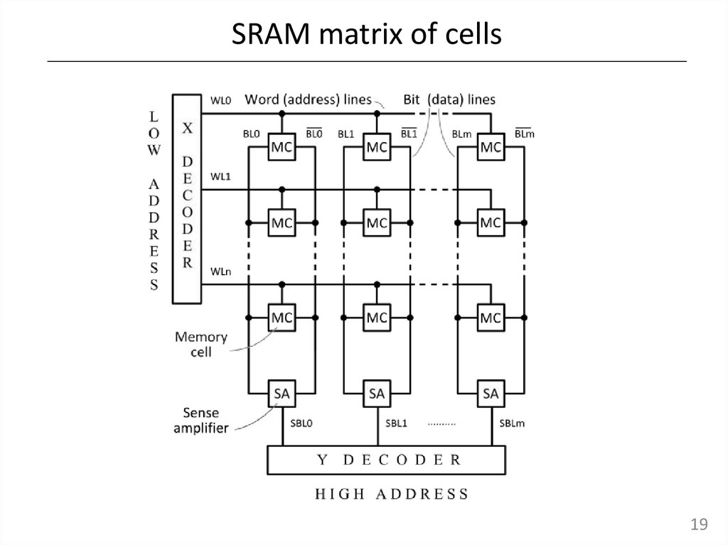
SRAM organizationSRAM memory cells are organized in a form of a matrix where
they are located in the intersection points of the horizontal
word lines WL and vertical bit lines BL. The word lines are
single-ended while the bit-lines are differential (implemented
as pairs of two complementary signals BL and NOT BL).
To access the memory cells, the full address (a combination of
the address lines) is divided into two parts – low X and high Y.
These combinations are converted into single active lines (row
and column) by X and Y address decoders.
18
19.
SRAM matrix of cells19
20.
SRAM operationSRAMs require a few control signals:
CS (chip select) – controls the access to the memory chip
(usually when CS=0 the access is enabled)
R/W (read/write) – configures the memory for read (R/W=1)
or write (R/W=0) operation
ОЕ (output enable) – enables/disables the memory output
buffers
20
21.
READ operation21
22.
WRITE operation22