Similar presentations:
Placement and routing guidelines for Power Electronics Devices
1. Placement and routing guidelines for Power Electronics Devices
Printed Circuit Board Design forPower Electronics: A Practical Guide
Dr. Oleksandr Velihorskyi, PhD
1
2. Lecture plan
Planning the layout.Single-board PCB layout.
Placement of Layers for PE devices.
Current loops in Power Electronics Devices.
Grounding in the PE devices.
Land Patterns for SMD components in PE devices.
Control scheme layout consideration.
2
3. Current position: 1/7
Planning the layout.Single-board PCB layout.
Placement of Layers for PE devices.
Current loops in Power Electronics Devices.
Grounding in the PE devices.
Land Patterns for SMD components in PE devices.
Control scheme layout consideration.
3
4. PCB design for PE devices. Why is it so important?
Improper PCB design leads to:"unstable" switching waveforms and jittering,
audible noise from the magnetic components,
ringing, crosstalk, ground bounce,
PCB design can lead good scheme to fail.
but even best PCB design can’t improve bad
schematic solution.
4
5. Planning the layout.
Each PE device contains power part and controlscheme.
Power part - DC/DC, DC/AC, AC/AC.
Control - measure parameters and generate signals.
Type of signals in the PE devices:
analog – measured values (control) - victims,
digital – control signals, interface with the
environment (PC, memory, etc.) – aggressors/victims,
power – DC or AC, sine, pulse - aggressors.
5
6. Planning the layout.
Do we need to separate power and control on totwo different PCB’s?
device characteristics?
EMC?
accuracy?
maintainability?
cost?
reliability?
6
7. Planning the layout.
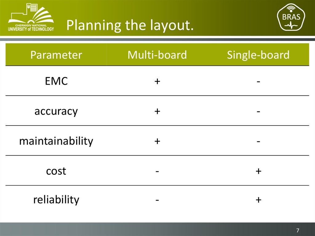
ParameterMulti-board
Single-board
EMC
+
-
accuracy
+
-
maintainability
+
-
cost
-
+
reliability
-
+
7
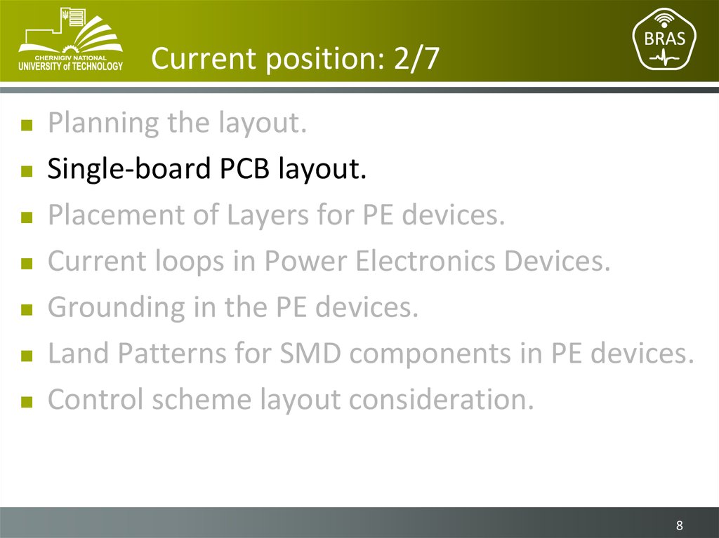
8. Current position: 2/7
Planning the layout.Single-board PCB layout.
Placement of Layers for PE devices.
Current loops in Power Electronics Devices.
Grounding in the PE devices.
Land Patterns for SMD components in PE devices.
Control scheme layout consideration.
8
9. Single-board PCB layout.
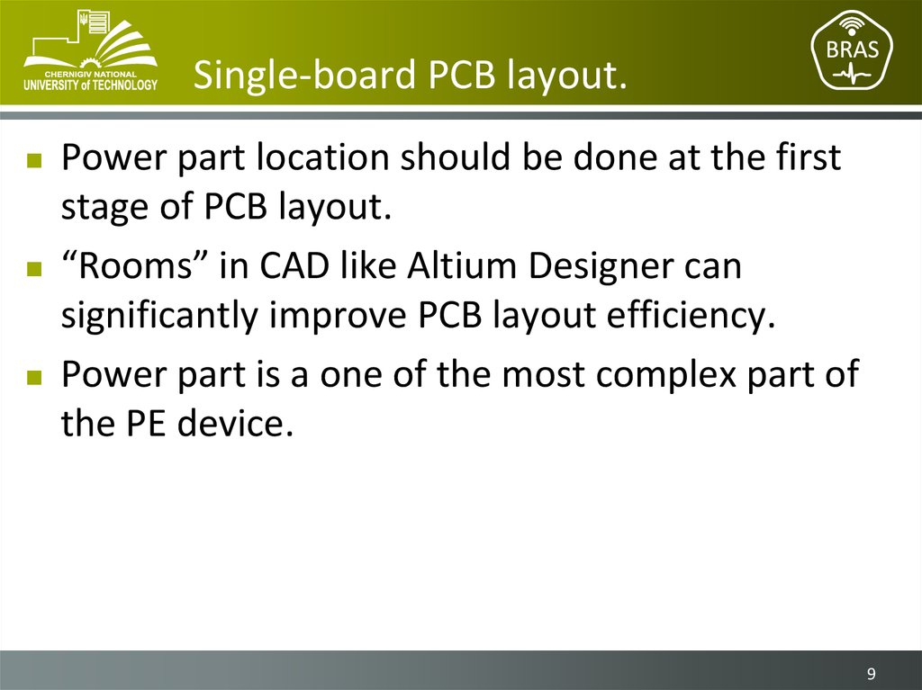
Power part location should be done at the firststage of PCB layout.
“Rooms” in CAD like Altium Designer can
significantly improve PCB layout efficiency.
Power part is a one of the most complex part of
the PE device.
9
10. Single-board PCB layout.
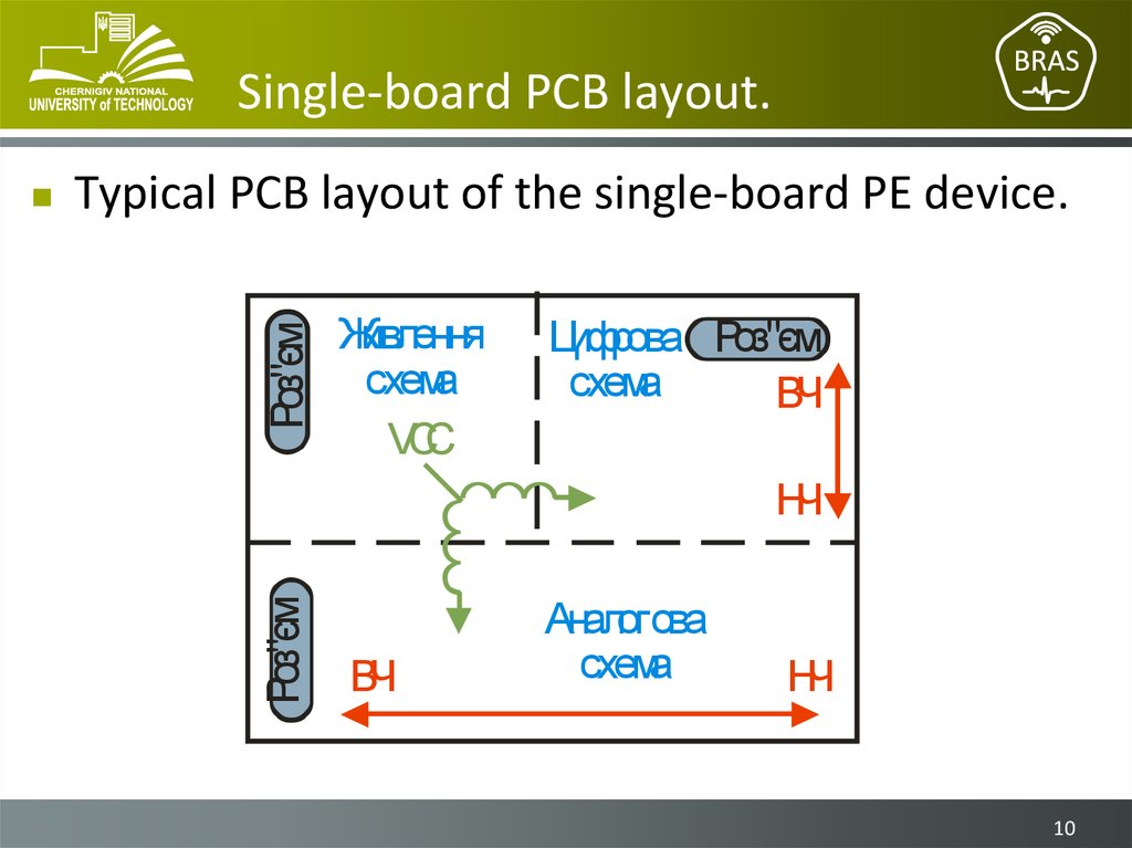
Роз"ємTypical PCB layout of the single-board PE device.
Живлення
схема
VCC
Цифрова Роз"єм
схема
ВЧ
НЧ
Роз"єм
ВЧ
Аналогова
схема
НЧ
10
11. Single-board PCB layout.
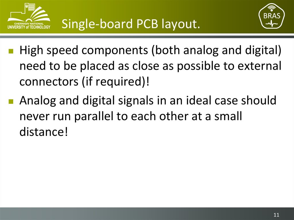
High speed components (both analog and digital)need to be placed as close as possible to external
connectors (if required)!
Analog and digital signals in an ideal case should
never run parallel to each other at a small
distance!
11
12. Current position: 3/7
Planning the layout.Single-board PCB layout.
Placement of Layers for PE devices.
Current loops in Power Electronics Devices.
Grounding in the PE devices.
Land Patterns for SMD components in PE devices.
Control scheme layout consideration.
12
13. Stack of layers – 1, 2 or more?
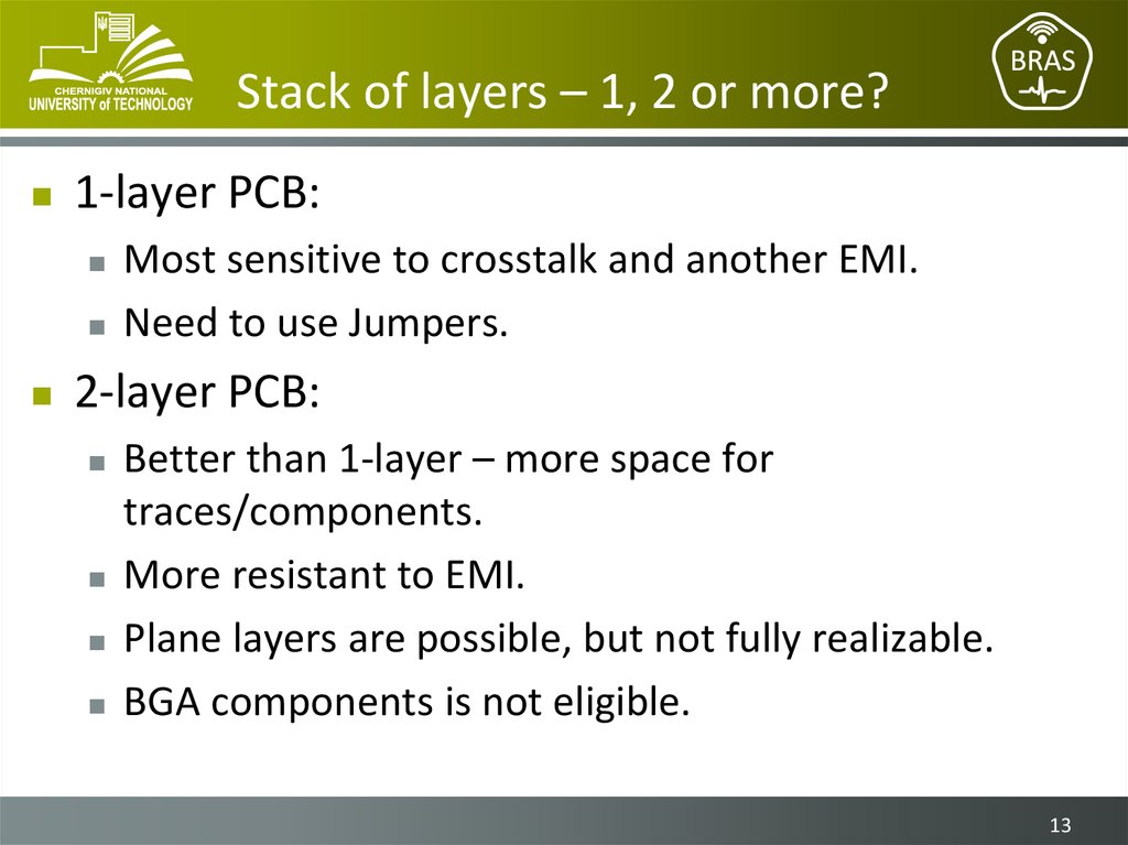
1-layer PCB:Most sensitive to crosstalk and another EMI.
Need to use Jumpers.
2-layer PCB:
Better than 1-layer – more space for
traces/components.
More resistant to EMI.
Plane layers are possible, but not fully realizable.
BGA components is not eligible.
13
14. Stack of layers – 1, 2 or more?
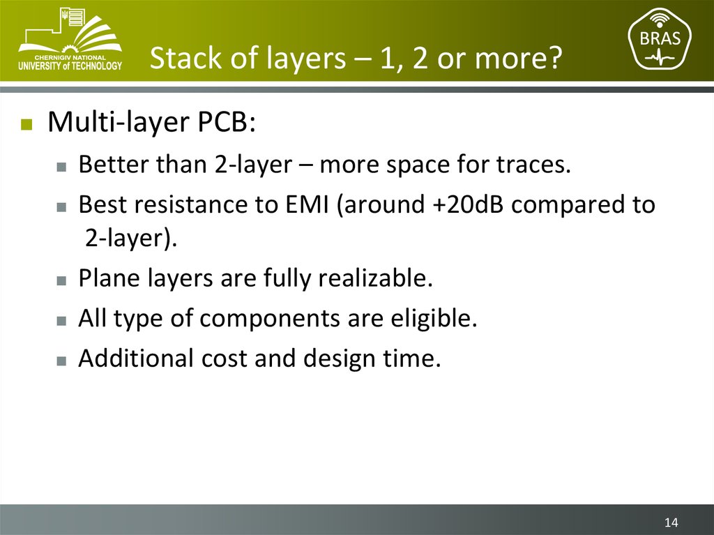
Multi-layer PCB:Better than 2-layer – more space for traces.
Best resistance to EMI (around +20dB compared to
2-layer).
Plane layers are fully realizable.
All type of components are eligible.
Additional cost and design time.
14
15. Stack of layers – 1, 2 or more?
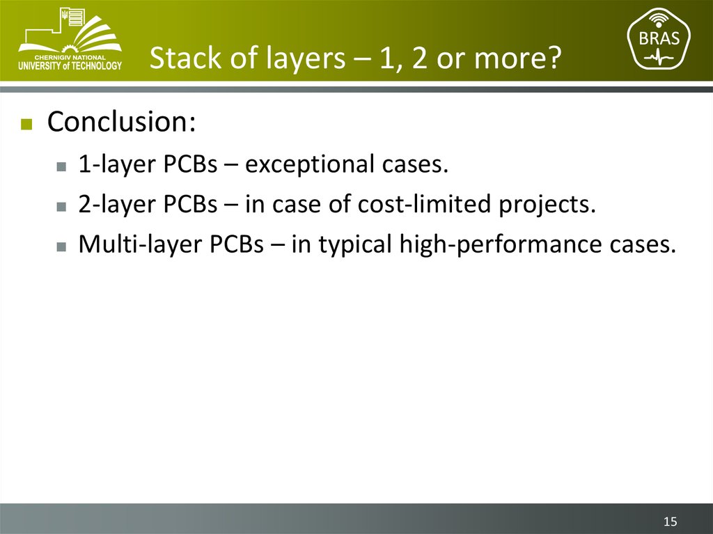
Conclusion:1-layer PCBs – exceptional cases.
2-layer PCBs – in case of cost-limited projects.
Multi-layer PCBs – in typical high-performance cases.
15
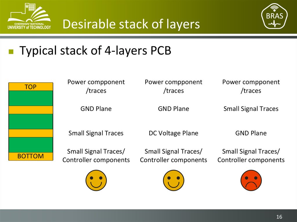
16. Desirable stack of layers
Typical stack of 4-layers PCBTOP
BOTTOM
Power compponent
/traces
Power compponent
/traces
Power compponent
/traces
GND Plane
GND Plane
Small Signal Traces
Small Signal Traces
DC Voltage Plane
GND Plane
Small Signal Traces/
Controller components
Small Signal Traces/
Controller components
Small Signal Traces/
Controller components
16
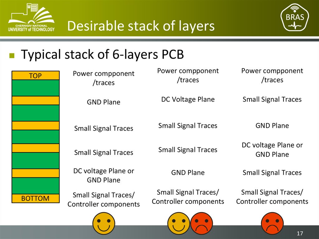
17. Desirable stack of layers
Typical stack of 6-layers PCBTOP
BOTTOM
Power compponent
/traces
Power compponent
/traces
Power compponent
/traces
GND Plane
DC Voltage Plane
Small Signal Traces
Small Signal Traces
Small Signal Traces
GND Plane
Small Signal Traces
Small Signal Traces
DC voltage Plane or
GND Plane
DC voltage Plane or
GND Plane
GND Plane
Small Signal Traces
Small Signal Traces/
Controller components
Small Signal Traces/
Controller components
Small Signal Traces/
Controller components
17
18. Current position: 4/7
Planning the layout.Single-board PCB layout.
Placement of Layers for PE devices.
Current loops in Power Electronics Devices.
Grounding in the PE devices.
Land Patterns for SMD components in PE devices.
Control scheme layout consideration.
18
19. Important features of power part
Highest currents and voltages in the deviceWhat ever – mA and V or A and kV.
Traces width and clearances should be wide enough!
Large current pulses with sharp edges.
Sharp edges leads to electromagnetic interference
(EMI).
PCB designer must pay attention to the each
switching circuits in PE device – identify, place
components and properly route traces!
19
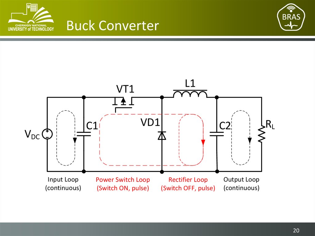
20. Buck Converter
L1VT1
C1
VDC
Input Loop
(continuous)
VD1
Power Switch Loop
(Switch ON, pulse)
C2
Rectifier Loop
(Switch OFF, pulse)
RL
Output Loop
(continuous)
20
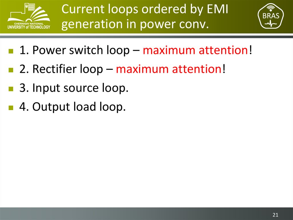
21. Current loops ordered by EMI generation in power conv.
1. Power switch loop – maximum attention!2. Rectifier loop – maximum attention!
3. Input source loop.
4. Output load loop.
21
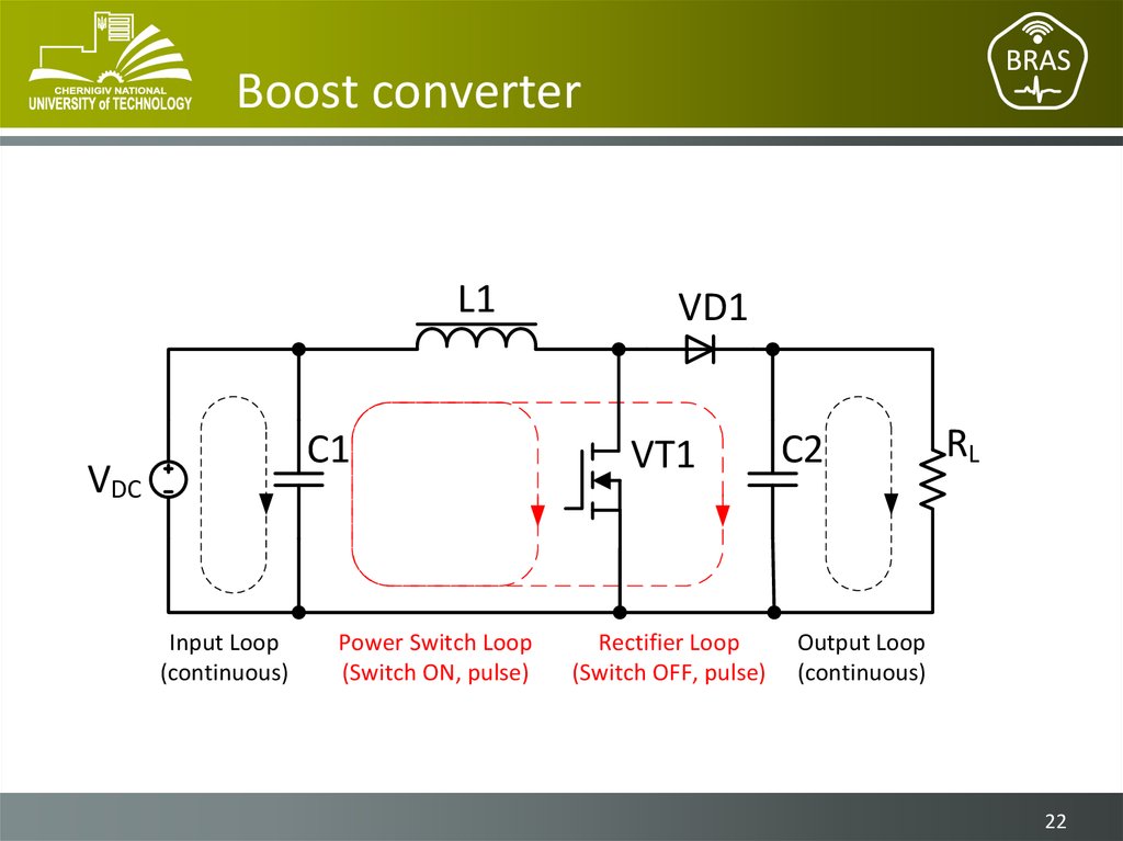
22. Boost converter
L1C1
VDC
Input Loop
(continuous)
Power Switch Loop
(Switch ON, pulse)
VD1
VT1
Rectifier Loop
(Switch OFF, pulse)
C2
RL
Output Loop
(continuous)
22
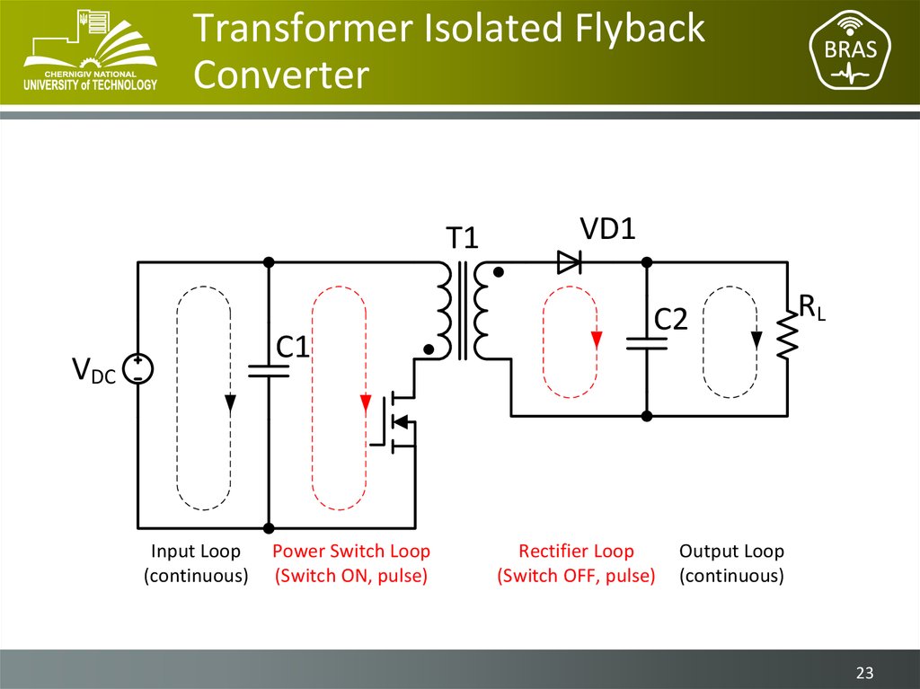
23. Transformer Isolated Flyback Converter
T1C1
VDC
Input Loop
(continuous)
Power Switch Loop
(Switch ON, pulse)
VD1
C2
Rectifier Loop
(Switch OFF, pulse)
RL
Output Loop
(continuous)
23
24. The first rule for PE devices PCB design.
1. The pulse loop circumference must be as short aspossible.
traces with pulsating current must be as short and
wide as possible.
Results:
Trace resistance and inductance improvement.
EMI improvement (ΔU=L·di/dt).
Efficiency improvement (Ptrace=I2R).
24
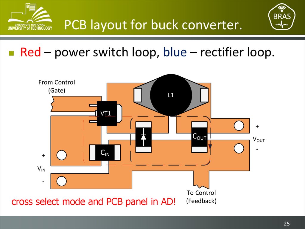
25. PCB layout for buck converter.
Red – power switch loop, blue – rectifier loop.From Control
(Gate)
L1
VT1
+
COUT
G
G
+
CGIN
VOUT
-
VIN
-
cross select mode and PCB panel in AD!
To Control
(Feedback)
25
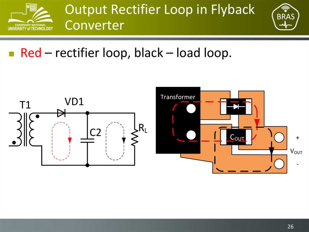
26. Output Rectifier Loop in Flyback Converter
Red – rectifier loop, black – load loop.T1
Transformer
VD1
G
C2
RL
G
COUT
+
VOUT
-
26
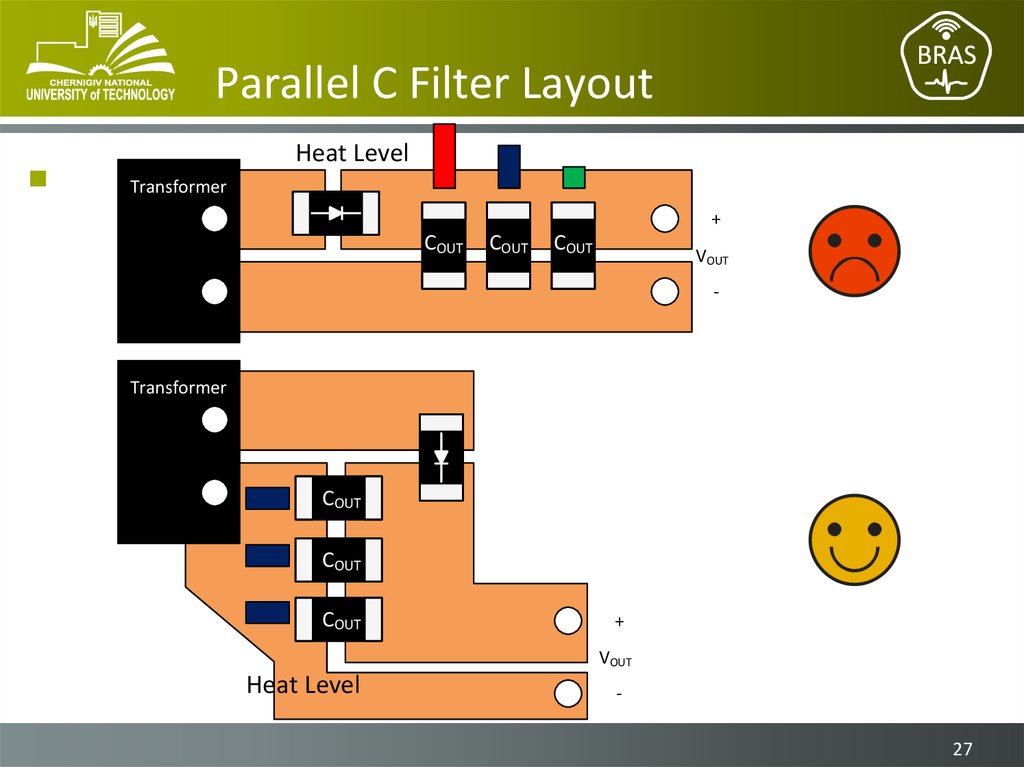
27. Parallel C Filter Layout
TransformerG
+
COUT
G
COUT
G
COUT
G
Heat Level
VOUT
-
Transformer
G
G
COUT
G
COUT
G
COUT
+
VOUT
Heat Level
-
27
28. Parallel C Filter Layout
PCB layout between each capacitor and source inmulti-component filter must be as identical as
possible!
Non-identical layout will lead to different current
sharing and will reduce capacitor lifespan (mean
time between failures, MTBF).
28
29. Current position: 5/7
Planning the layout.Single-board PCB layout.
Placement of Layers for PE devices.
Current loops in Power Electronics Devices.
Grounding in the PE devices.
Land Patterns for SMD components in PE devices.
Control scheme layout consideration.
29
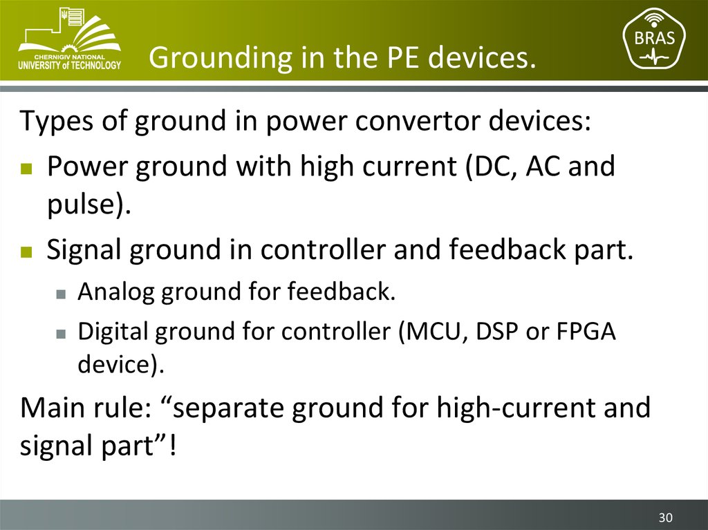
30. Grounding in the PE devices.
Types of ground in power convertor devices:Power ground with high current (DC, AC and
pulse).
Signal ground in controller and feedback part.
Analog ground for feedback.
Digital ground for controller (MCU, DSP or FPGA
device).
Main rule: “separate ground for high-current and
signal part”!
30
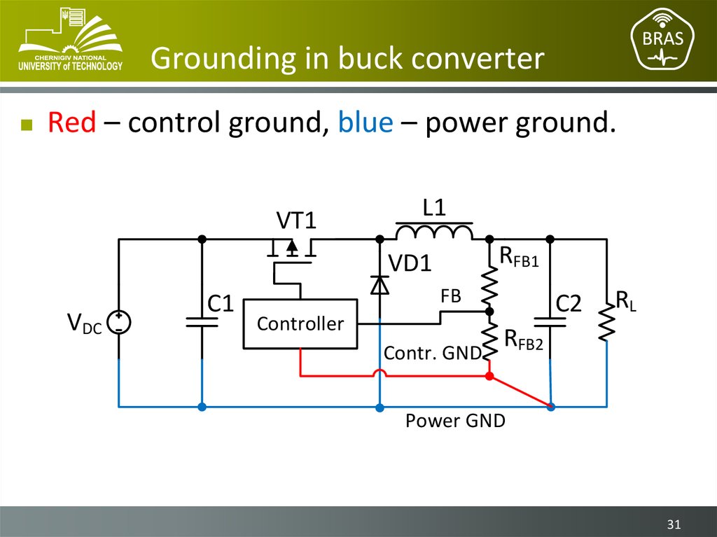
31. Grounding in buck converter
Red – control ground, blue – power ground.VT1
L1
RFB1
VD1
VDC
C1
FB
Controller
Contr. GND
C2
RL
RFB2
Power GND
31
32. Control and power ground connection.
Rules of thumb for grounding in PE devices:Feedback ground must be connected with power
ground near the negative pin of output capacitor.
If control IC has separated (power and control)
ground, these pins must be routed separately
and connected to the current sensing resistor
that measure power switch current.
32
33. Grounding in flyback converter
T1VDC
RL
RFB1
C1
Controller
VD1
FB
C2
VT1
RCS
RFB2
VD1
Output GND
Contr. GND
Input GND
33
34. Current position: 6/7
Planning the layout.Single-board PCB layout.
Placement of Layers for PE devices.
Current loops in Power Electronics Devices.
Grounding in the PE devices.
Land Patterns for SMD components in PE devices.
Control scheme layout consideration.
34
35. Current sensor resistor PCB layout consideration
The best characteristic provides 4-wire Kelvinsensing.
Example of using 2-wire resistors as 4-wire Kelvin
Current sensor
Current sensor
Power polygons
Sensor Traces
Sensor Traces
35
36. Current sensor resistor PCB layout consideration
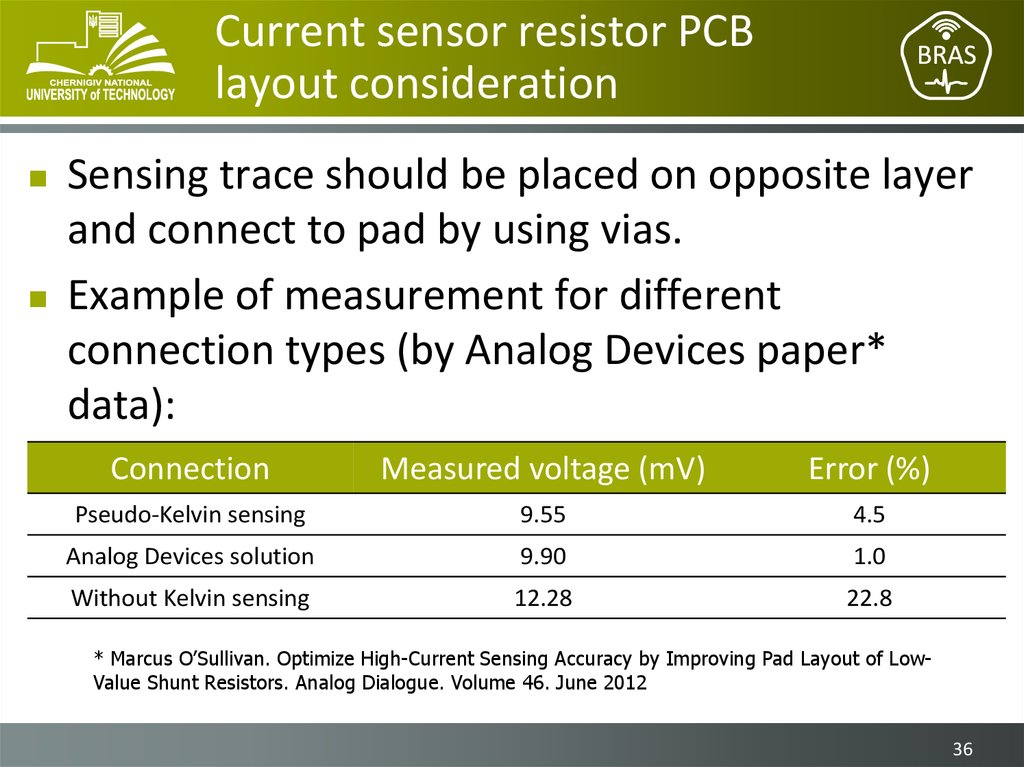
Sensing trace should be placed on opposite layerand connect to pad by using vias.
Example of measurement for different
connection types (by Analog Devices paper*
data):
Connection
Measured voltage (mV)
Error (%)
Pseudo-Kelvin sensing
9.55
4.5
Analog Devices solution
9.90
1.0
Without Kelvin sensing
12.28
22.8
* Marcus O’Sullivan. Optimize High-Current Sensing Accuracy by Improving Pad Layout of LowValue Shunt Resistors. Analog Dialogue. Volume 46. June 2012
36
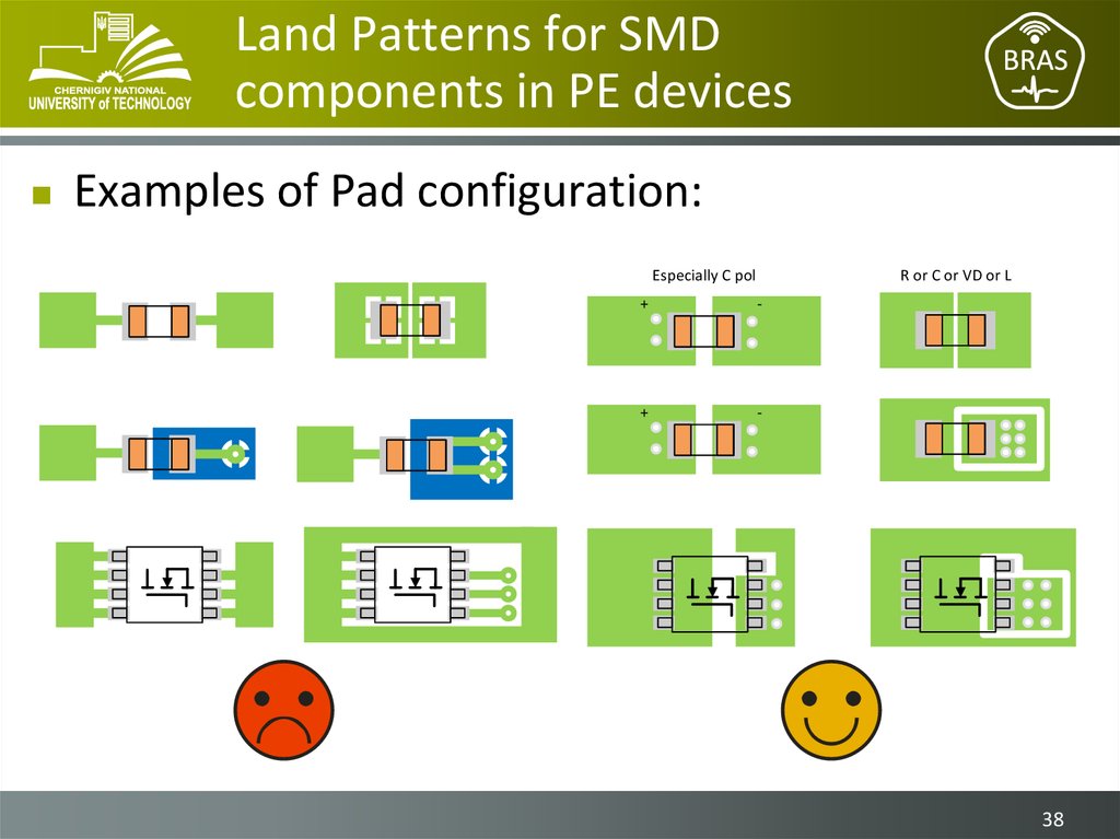
37. Land Patterns for SMD components in PE devices
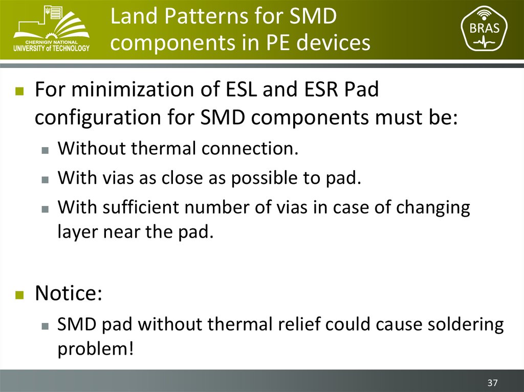
For minimization of ESL and ESR Padconfiguration for SMD components must be:
Without thermal connection.
With vias as close as possible to pad.
With sufficient number of vias in case of changing
layer near the pad.
Notice:
SMD pad without thermal relief could cause soldering
problem!
37
38. Land Patterns for SMD components in PE devices
Examples of Pad configuration:Especially C pol
R or C or VD or L
+
-
+
-
38
39. Current position: 7/7
Planning the layout.Single-board PCB layout.
Placement of Layers for PE devices.
Current loops in Power Electronics Devices.
Grounding in the PE devices.
Land Patterns for SMD components in PE devices.
Control scheme layout consideration.
39
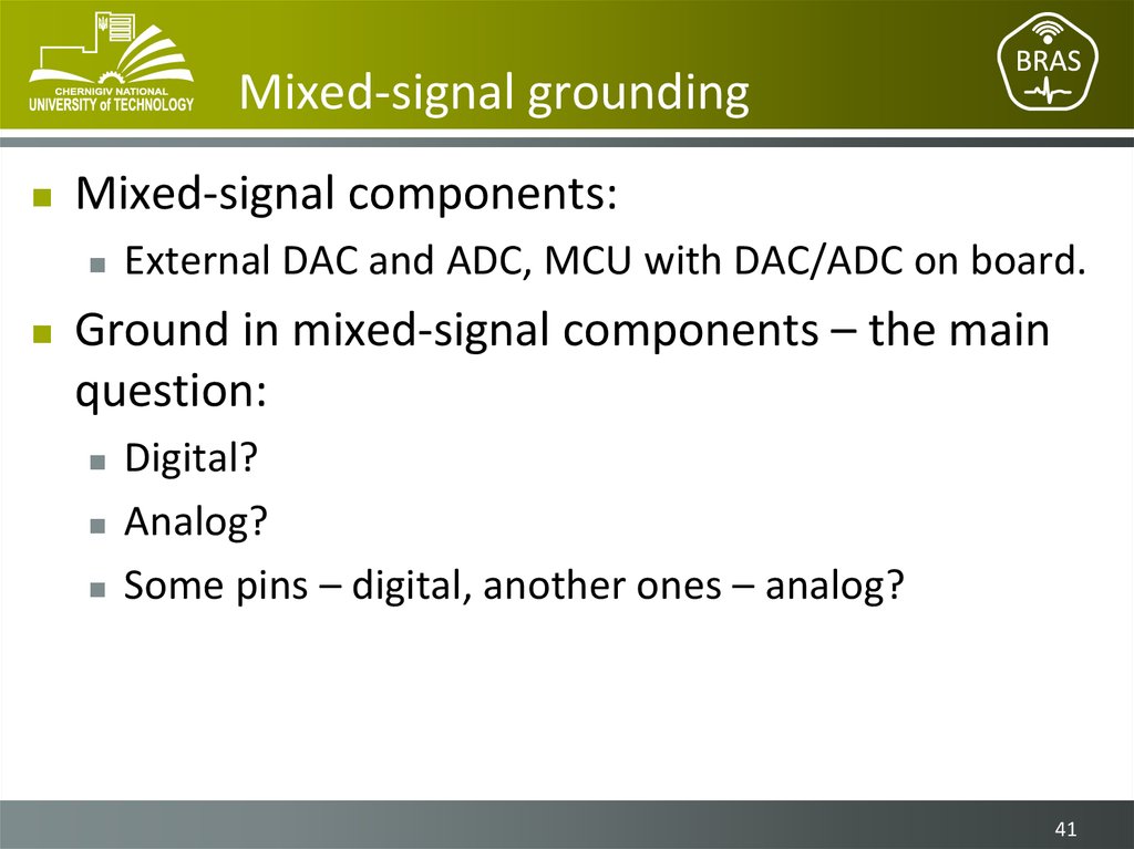
40. Mixed-signal grounding
Mixed-signal components:External DAC and ADC, MCU with DAC/ADC on board.
Ground in mixed-signal components – the main
question:
Digital?
Analog?
Some pins – digital, another ones – analog?
40
41. Mixed-signal grounding
Mixed-signal components:External DAC and ADC, MCU with DAC/ADC on board.
Ground in mixed-signal components – the main
question:
Digital?
Analog?
Some pins – digital, another ones – analog?
41
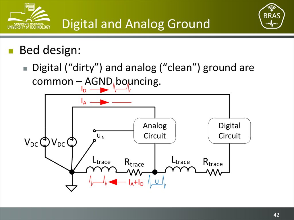
42. Digital and Analog Ground
Bed design:Digital (“dirty”) and analog (“clean”) ground are
common – AGND bouncing.
ID
IA
VDC
VDC
UIN
Ltrace
Analog
Circuit
Ltrace
Rtrace
IA+ID
Digital
Circuit
Rtrace
U
42
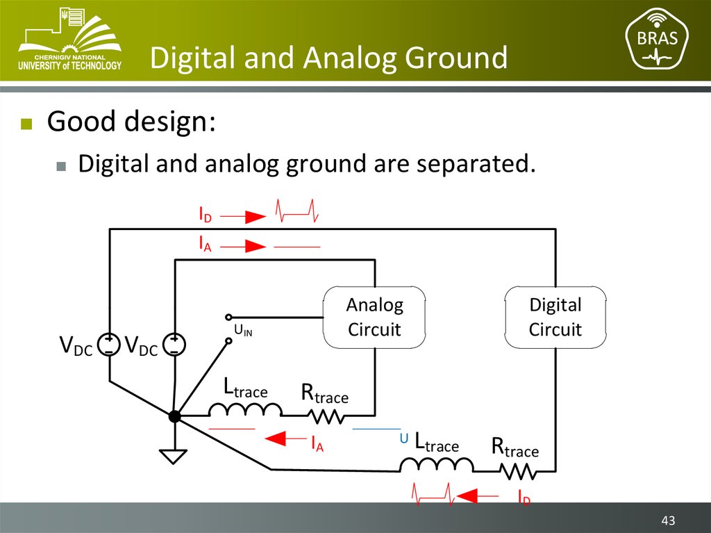
43. Digital and Analog Ground
Good design:Digital and analog ground are separated.
ID
IA
VDC
VDC
Analog
Circuit
UIN
Ltrace
Digital
Circuit
Rtrace
IA
U
Ltrace
Rtrace
ID
43
44. Digital and Analog Ground
Planes for ground in control circuits of powerelectronic devices should improve EMC of control
circuit.
4-layer PCB (sig - VCC– GND - sig) is a typical
solution for the control board.
VCC and GND planes provide additional
distributed capacitance for control board power
supply.
44
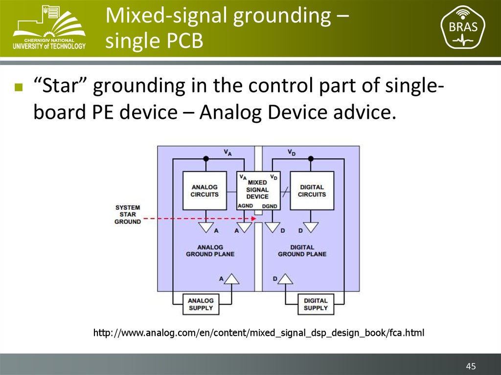
45. Mixed-signal grounding – single PCB
“Star” grounding in the control part of singleboard PE device – Analog Device advice.http://www.analog.com/en/content/mixed_signal_dsp_design_book/fca.html
45
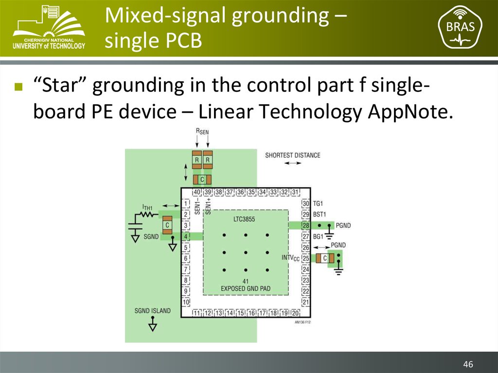
46. Mixed-signal grounding – single PCB
“Star” grounding in the control part f singleboard PE device – Linear Technology AppNote.46
47. Mixed-signal grounding – multi-board PCB
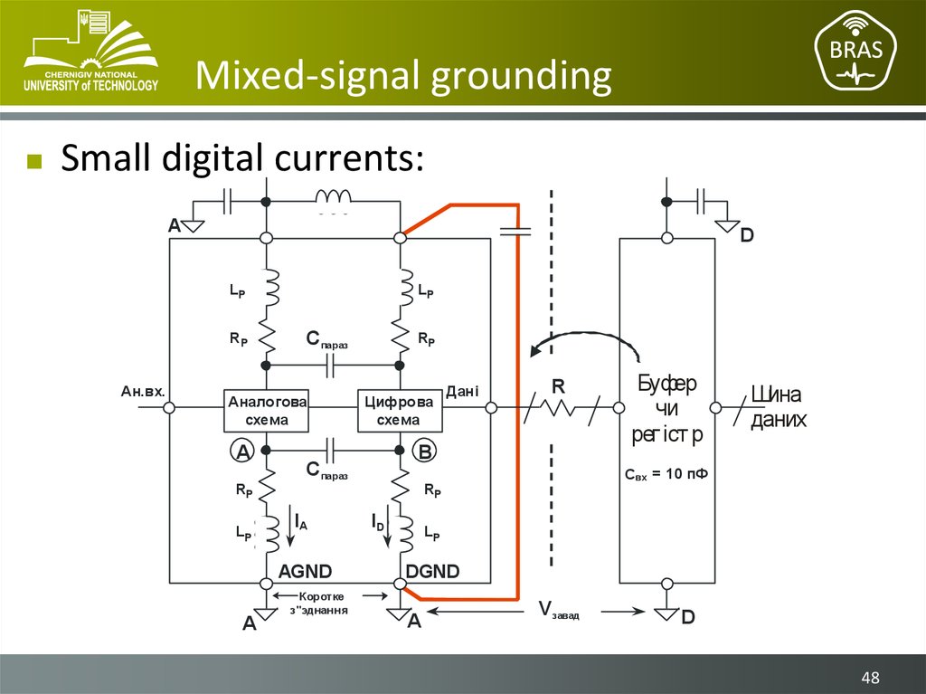
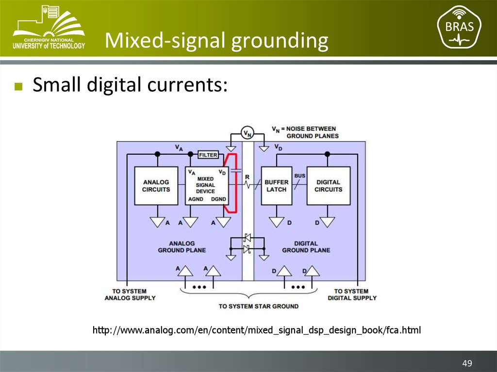
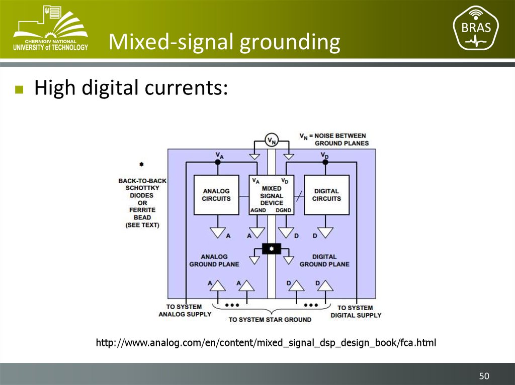
Grounding techniques for single-board PE devicesare not optimum for multi-board devices.
Multi-board grounding techniques are depend on
Low digital currents.
High digital currents.
Provide additional ground pin in the connectors.
Recommend allocate 30-40% connector pins to GND.
Separate digital and analog signals by ground pins.
47
48. Mixed-signal grounding
Small digital currents:A
D
LP
LP
RP
Ан.вх.
Cпараз
Аналогова
схема
A
RP
Цифрова
схема
Буфер
чи
рег іст р
Шина
даних
Cвх = 10 пФ
RP
IA
AGND
A
R
B
Cпараз
RP
LP
Дані
Коротке
з"эднання
ID
LP
DGND
A
Vзавад
D
48
49. Mixed-signal grounding
Small digital currents:http://www.analog.com/en/content/mixed_signal_dsp_design_book/fca.html
49
50. Mixed-signal grounding
High digital currents:http://www.analog.com/en/content/mixed_signal_dsp_design_book/fca.html
50
51. Bypass Capacitors
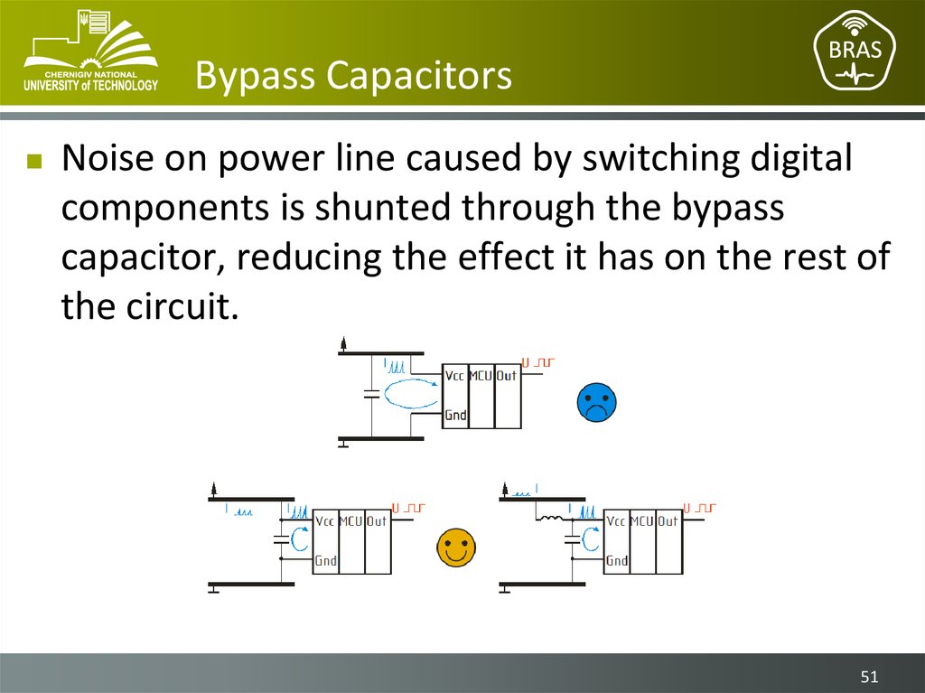
Noise on power line caused by switching digitalcomponents is shunted through the bypass
capacitor, reducing the effect it has on the rest of
the circuit.
51
52. Bypass Capacitors
Bypass capacitor should be connected to thepower pins of the digital components as close as
possible!
52
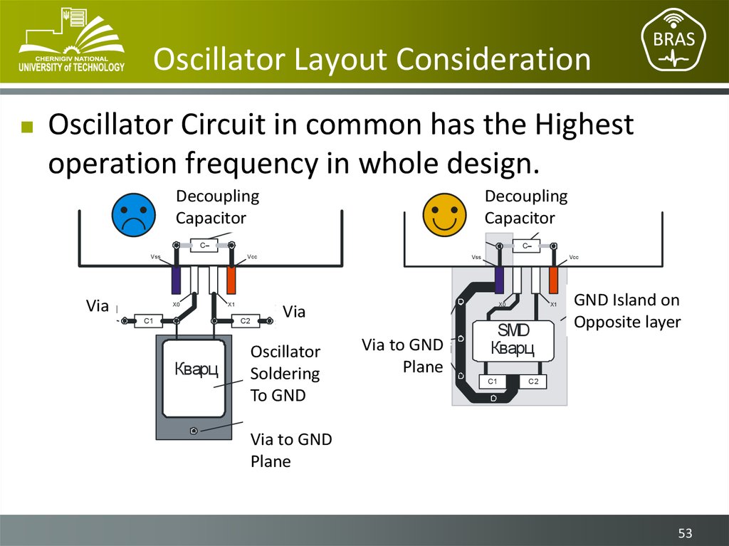
53. Oscillator Layout Consideration
Oscillator Circuit in common has the Highestoperation frequency in whole design.
Decoupling
Фільт р. конд
Capacitor
з зовн. боку ДП
Decoupling
Фільт р. конд
Capacitor
з зовн. боку ДП
C
C
Vss
Via
З"єднання
з землею
Vcc
X0
C1
X1
C2
Кварц
Vss
З"єднання
Via
з землею
Oscillator
Кварц
Soldering
припаяний
до
землі
To зGND
Перех. от вір
до шару землі
Vcc
X0
Перех. от вір
Via
to GND
до шару
землі
X1
SMD
Кварц
Ост
рівець
GND
GND
Island
on
з зовн. боку ДП
Opposite layer
Plane
C1
C2
Via to GND
Plane
53









 internet
 electronics


