


")


 electronics
Similar presentations:


Linear Power: Low Dropout Regulators
1. Linear Power: Low Dropout Regulators
STB and MediaJose Gonzalez – Product Marketing Engineer
TI Information – Selective Disclosure
1
2. Use Cases and Block Diagrams: STB
LDOWi-fi
12 – 14V
Adapter
Bluetooth
DC/DC
Converter
Power/Battery Management
Low noise
power rail
LDO
LDO
ESD
LDO
EN
Step-Down Power supply
EN
Wireless Interface
HDMI/USB
Low noise power rail
LDO
EN
Tuner
Audio Codec
Audio
Switch
LDO
Zapper
EN
IN
SSD
SSDCell
CellCell
Memory
LDO
DDR3/4
Audio
Amp
AON
Audio
Power
Good
SSD/HDD/SD
Primary LDO Use
HOME
TI Information – Selective Disclosure
Typically used for low-dropout conditions or low current
demand with emphasis on low noise and low standby power
2
3.
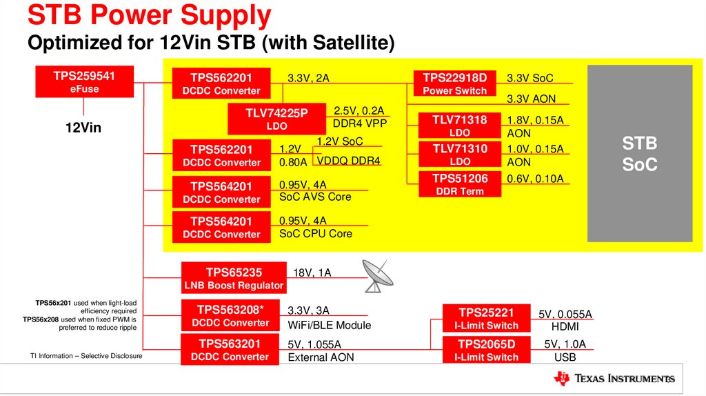
STB Power SupplyOptimized for 12Vin STB (with Satellite)
TPS259541
TPS562201
eFuse
DCDC Converter
Power Switch
TLV74225P
12Vin
TPS22918D
3.3V, 2A
LDO
TPS562201
DCDC Converter
TPS564201
DCDC Converter
TPS564201
DCDC Converter
2.5V, 0.2A
DDR4 VPP
1.2V SoC
1.2V
0.80A VDDQ DDR4
0.95V, 4A
SoC AVS Core
TLV71318
3.3V SoC
3.3V AON
LDO
1.8V, 0.15A
AON
1.0V, 0.15A
AON
TPS51206
0.6V, 0.10A
LDO
TLV71310
STB
SoC
DDR Term
0.95V, 4A
SoC CPU Core
TPS65235
18V, 1A
LNB Boost Regulator
TPS56x201 used when light-load
efficiency required
TPS56x208 used when fixed PWM is
preferred to reduce ripple
TPS563208*
DCDC Converter
TPS563201
TI Information – Selective Disclosure
DCDC Converter
3.3V, 3A
WiFi/BLE Module
I-Limit Switch
5V, 1.055A
External AON
I-Limit Switch
TPS25221
TPS2065D
5V, 0.055A
HDMI
5V, 1.0A
USB
3
4.
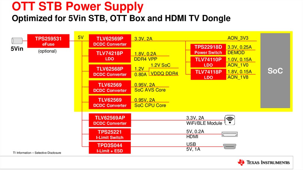
OTT STB Power SupplyOptimized for 5Vin STB, OTT Box and HDMI TV Dongle
TPS259531
5Vin
5V
TLV62569P
eFuse
DCDC Converter
(optional)
TLV74218P
LDO
TLV62568P
DCDC Converter
TLV62569
DCDC Converter
TLV62569
DCDC Converter
TLV62569AP
DCDC Converter
TPS25221
I-Limit Switch
TPD3S044
TI Information – Selective Disclosure
I-Limit + ESD
AON_3V3
3.3V, 2A
TPS22918D
1.8V, 0.2A
DDR4 VPP
1.2V SoC
1.2V
0.80A VDDQ DDR4
Power Switch
TLV74110P
LDO
TLV74118P
LDO
3.3V, 0.25A
DEMOD
1.0V, 0.15A
AON_1V0
1.8V, 0.15A
AON_1V8
SoC
0.95V, 2A
SoC AVS Core
0.95V, 2A
SoC CPU Core
3.3V, 2A
WiFi/BLE Module
5V, 0.2A
HDMI
USB
5V, 1A
4
5. LDO Power Solutions Value Line LDOs and Lin Regs
DevelopmentReleased/Sampling
TLV760
>2x2
100mA, 4.2V-30V
SOT23
TLV703
300mA, 2V-5.5V
SOT23
TLV704
2x2
150mA, 2.5V-24V
SOT23
TLV757P
TLV759P (adj)
1x1
1A, 1.4V-5.5V
2x2, SOT23
IOUT
TLV741P
TLV713/P
TLV742P
TLV707
TLV743P
TLV733P
150mA, 1.4V-5.5V
1x1, SOT23
200mA, 2V-5.5V
1x1
300mA, 1.4V-5.5V
1x1, SOT23
150mA
200mA
TI Information – Selective Disclosure
300mA
TLV755P
TLV758P(adj)
500mA, 1.4V-5.5V
1x1, SOT23, 2X2
500mA
1A
5
6. LDO Power Solutions Capacitor-Free LDOs (MLCC Shortage Solution)
TLV713P and TLV733P Can work withoutinput and output capacitors
Layout Example
Vout
Vin
DQN
LDO
(1x1mm)
GND
Optional
EN
EN
Second layer
connection
Optional
Performance and Space Savings
Ceramic Capacitor (MLCC) Shortage (2018)
The 2018 market in 1H has created a challenge for designs in
portable electronics. The lead-times for the industry could cause
delays in delivery and manufacturing.
If the power supply operating frequency is below or at 100KHz
the PSRR of the TLV733 can behave very well for easy low
current loads. If a higher frequency is needed then a capacitor
would be recommended
LDOs can help alleviate the burden by working with no
capacitors!
Having no capacitors in the input/output also saves on
space!
TI Information – Selective Disclosure
6
7. LDO Power Solutions Replacing TLV1117 with TLV766/7
TLV1117**800mA
Up to 18VIN
TLV766**
TLV767**
500mA
1A
Development
Sampling
Released
Improvements From TLV1117 to TLV766/7
Lower IQ: From 5000 µA to 50 µA
Smaller Size : From 6.5mmx3.5mm to 2mmx2mm
Improved Reliability : Added Fold-back Current Limiting
Dropout Voltage @100mA : From 1.1V to ~140mV
Lower VOUT Capability : From 1.25 to 0.8V
Added Enable
EN
Up to 6VIN
TLV1117LV**
1A
*Adjustable Output
**Fixed/Adjustable Output
TI Information – Selective Disclosure
TLV755P
TLV758P*
500mA
500mA
Improvements From TLV1117LV to TLV75x
Lower IQ: from 100µA to 20 µA
Smaller Size : From 6.5mmx3.5mm to 1mmx1mm
Dropout Voltage 1A: From 800mV to 475mV
Lower VOUT Capability : From 1.25 to 0.6V
TLV757P
TLV759P*
1A
1A
7
8. Use Cases and Block Diagrams: STB
LDOWi-fi
12 – 14V
Adapter
Bluetooth
DC/DC
Converter
Power/Battery Management
Low noise
power rail
LDO
LDO
ESD
LDO
EN
Step-Down Power supply
EN
Wireless Interface
HDMI/USB
Low noise power rail
Tuner
LDO
EN
EN
Audio Codec
LDO
Audio
Switch
Zapper
IN
SSD
SSDCell
CellCell
Memory
LDO
DDR3/4
Audio
Amp
AON
Audio
Power
Good
SSD/HDD/SD
Primary LDO Use
HOME
TI Information – Selective Disclosure
Typically used for low-dropout conditions or low current
demand with emphasis on low noise and low standby power
8
9. Use Cases and Block Diagrams: STB
Power Management and Battery SubsystemLow noise
powerarail
LDOs areWi-fi
used to provide
low drop power rail or direct
LDOoutput.
from battery power rail which provides a low noise
This isBluetooth
used to power LDO
peripherals such as touch-bars,
additional communication modules, etc. LDO are also used
ESD
for the Display power.
Standby Power
LDO
12 – 14V
Adapter
DC/DC
Converter
Power/Battery Management
LDO
EN
Step-Down Power supply
Low noise power rail
LDO
Audio Codec
LDO
EN
Audio
Audio
Switch
Audio
Amp
Typical Voltage Ranges: EN
Wireless
5.5V
→ 5V Interface
5V, 4.2V → 3.3V
3.3V, 2.5V, → 1.8V
1.8V → 1.2V
Tuner
EN
Key Concerns
• Low IQ
•Zapper
Wide VIN
IN
• Enable/Shutdown
HDMI/USB
SSD
SSDCell
CellCell
Memory
LDO
DDR3/4
Power
AON
Key
Devices:
Good
High Performance
• TLV757P: 1A, IQ: 20μA, Fold-back Current Limit
• TPS709: 0.15A, 30VIN,SSD/HDD/SD
Reverse Current Protection.
• TLV707P: 0.2A, 50dB PSRR @ 1MHz, 0.5% Accuracy
• TPS7A25: 0.3A, 18VIN, , Power Good.
Value Line
• TLV713/741: 0.15A, 230mVDROP, Cap-less Stable
• TLV733/743: 0.3A, 125mVDROP, Cap-less Stable
• TLV704: 0.15A, 24VIN, IQ: 3.2 μA
low• current
TLV705: 0.2A, 105mVDROP, Ultra-low profile pkg
Primary LDO Use
HOME
TI Information – Selective Disclosure
Typically used for low-dropout conditions or
demand with emphasis on low noise and low standby power
9
10. Use Cases and Block Diagrams: STB
HDMI/USB/Tuner/Zapper/Wifi/BluetoothThese analog rails need to send clean digital signals to their
LDO
respective outputs. These signals in turn are very susceptible to
12 –which
14V means selecting devices with low noise, high PSRR
noise
andAdapter
low IQ are important factors..
DC/DC
LDO
Converter
Typical Voltage Ranges:
5V → 3.3V
Power/Battery5VManagement
→ 2.5V
Step-Down Power supply
Key Concerns
• Low VDROP
• Small package area
• Low Noise
LDO
• Low IQ
Key Devices:
EN
Wi-fi
Bluetooth
Low noise
power rail
LDO
LDO
ESD
EN
EN
Wireless Interface
HDMI/USB
Low noise power rail
Tuner
EN
Audio Codec
Audio
Switch
LDO
Zapper
IN
SSD
SSDCell
CellCell
Memory
LDO
DDR3/4
Audio
2
TLV755: 0.5A, 220mVDROP, IQ: 15µA,
Amp 1mm
2
TLV757: 1A, 440mVDROP, IQ: 20µA, 4mm
TLV1117LV: 1A, 455mVDROP, 2.25mm2
TLV733P:Audio
0.3A, 125mVDROP, Cap-less Stable
TPS7A37: 1A, 1% accuracy, 4mm2
TPS748: 3A, 1% accuracy, 4mm2
AON
Power
Good
SSD/HDD/SD
Primary LDO Use
HOME
TI Information – Selective Disclosure
Typically used for low-dropout conditions or low current
demand with emphasis on low noise and low standby power
10
11. Use Cases and Block Diagrams: STB
Memory and DDR Power12 – 14V
Adapter
Power/Battery Management
LDO
EN
Audio
Low noise
LDO
SSD controllers and flash cells
are very sensitive to voltage Wi-fi
power rail
swings. Power for the cells and controllers is usually packed in
a space constrained board making pkg size very important.
Bluetooth
LDO
LDOs with very low dropdown in 1mm2 are preferred. Ultra-low
DC/DC
LDO
IQ is also important to maintain regulation
without draining the
Converter
battery. Power good signal is also used for resetting the SSD
EN
controller and notifying the PCIE host.
EN
Step-Down Power supply
Wireless Interface
Typical Voltage Ranges:
5.5V →rail
3.3V
Low noise power
3.3V, 4V → 2.5V
Tuner
3.3V, 2.5V, → 1.8V
EN
Audio Codec
Key Concerns
Zapper
• Low VDROP
IN
LDO
Audio • Small package area
Audio
Switch • Low
IQ
AmpGood
• Power
AON
Key Devices:
High Performance
• TPS74801: 1.5A, 60mVDROP, 9mm2, PG
• TLV700: 0.2A, 43mVDROP, 2.25mm2
• LP5912: 0.5A, 85mVDROP, 4mm2, PG
• TPS782: 0.15A, 130mVDROP, IQ: 500nA, 4mm2
LDO
ESD
HDMI/USB
SSD
SSDCell
CellCell
Memory
LDO
DDR3/4
Power
Good
SSD/HDD/SD
Primary LDO Use
HOME
TI Information – Selective Disclosure
Value Line
• TLV733P: 0.3A, 125mVDROP, Cap-less Stable
Typically
used for low-dropout conditions or low current
• TLV707P: 0.2A, 50dB PSRR @ 1MHz, 1mm2
demand
with
emphasis
on low
noise and low standby power
• TLV713P:
0.15A, 230mV
DROP, Cap-less Stable
11
12. Use Cases and Block Diagrams: STB
Audio Codec12 – 14V
Adapter
Power/Battery Management
LDO
EN
Audio
HOME
TI Information – Selective Disclosure
Low noise
LDO
powertorail
Wi-finoise power
LDOs are used to provide ultra low
the
audio codec to improve the sound quality of the speakers,
headphone and microphones.Bluetooth
Small Size LDOs
LDOare
desirable due to space constrained audio modules. High
DC/DC
LDO Audio has become a good selling feature for the
Fidelity
Converter
Note Books market.
EN
EN
Step-Down Power supply
Wireless Interface
Typical Voltage Ranges:
5.5V → 3.3V
Low noise power rail
3.3V, 4V → 2.5V
3.3V, 2.5V → 1.8V
Tuner
EN
Audio Codec
Key Concerns
Audio
Switch
Audio
Amp
Low Noise
LDO PSRR
High
Small package area
Zapper
IN
LDO
ESD
HDMI/USB
SSD
SSDCell
CellCell
Memory
LDO
DDR3/4
Power
AON
Key Devices:
Good
High Performance
• LP5907: 250mA, 6.5uV RMS Noise, 82dB PSRR
• LP5910: 300mA, 12uV RMS Noise, 75dB PSRR SSD/HDD/SD
• LP5912: 500mA, 12uV RMS, 75dB PSRR
• TPS720: 350mA, 48uV RMS, 85dB PSRR
Value Line
Primary
• LDO
TLV705P: Use
0.2A, 26uV RMS, 55dB PSRR @ 1MHz
TLV707P: 0.2A, 45uV RMS, 50dB PSRR @ 1MHz
Typically used for low-dropout
or low
• conditions
TLV702P: 0.15A,
48uVcurrent
RMS, 50dB PSRR @ 1MHz
demand with emphasis on low noise and low standby power
12
13.
STB Power SupplyOptimized for 12Vin STB (with Satellite)
TPS259541
TPS562201
eFuse
DCDC Converter
Power Switch
TLV74225P
12Vin
TPS22918D
3.3V, 2A
LDO
TPS562201
DCDC Converter
TPS564201
DCDC Converter
TPS564201
DCDC Converter
2.5V, 0.2A
DDR4 VPP
1.2V SoC
1.2V
0.80A VDDQ DDR4
0.95V, 4A
SoC AVS Core
TLV71318
3.3V SoC
3.3V AON
LDO
1.8V, 0.15A
AON
1.0V, 0.15A
AON
TPS51206
0.6V, 0.10A
LDO
TLV71310
STB
SoC
DDR Term
0.95V, 4A
SoC CPU Core
TPS65235
18V, 1A
LNB Boost Regulator
TPS56x201 used when light-load
efficiency required
TPS56x208 used when fixed PWM is
preferred to reduce ripple
TPS563208*
DCDC Converter
TPS563201
TI Information – Selective Disclosure
DCDC Converter
3.3V, 3A
WiFi/BLE Module
I-Limit Switch
5V, 1.055A
External AON
I-Limit Switch
TPS25221
TPS2065D
5V, 0.055A
HDMI
5V, 1.0A
USB
13
14.
OTT STB Power SupplyOptimized for 5Vin STB, OTT Box and HDMI TV Dongle
TPS259531
5Vin
5V
TLV62569P
eFuse
DCDC Converter
(optional)
TLV74218P
LDO
TLV62568P
DCDC Converter
TLV62569
DCDC Converter
TLV62569
DCDC Converter
TLV62569AP
DCDC Converter
TPS25221
I-Limit Switch
TPD3S044
TI Information – Selective Disclosure
I-Limit + ESD
AON_3V3
3.3V, 2A
TPS22918D
1.8V, 0.2A
DDR4 VPP
1.2V SoC
1.2V
0.80A VDDQ DDR4
Power Switch
TLV74110P
LDO
TLV74118P
LDO
3.3V, 0.25A
DEMOD
1.0V, 0.15A
AON_1V0
1.8V, 0.15A
AON_1V8
SoC
0.95V, 2A
SoC AVS Core
0.95V, 2A
SoC CPU Core
3.3V, 2A
WiFi/BLE Module
5V, 0.2A
HDMI
USB
5V, 1A
14
15. LDO for STBs/TV
Value/ HiPerformance
/New
GPN
SBE-2
Description
(Short)
Used for
(function
it
performs)
Pkg
size
Popular
TLV1117
The TLV1117 device is a
positive low-dropout voltage
regulator designed to provide
up to 800 mA of output current.
Power supply
for controller,
and I/o
4.00 ×
4.00
Value
TLV733P
TLV707P
TLV713P
The TLV733 series of LDOs
are ultra-small, low quiescent
current LDOs that can source
300 mA with good line and
load transient performance.
Powering
MCU, flash
memory and
other low
voltage rails
1.00
x
1.00
TPS735
The TPS735 family of LDOs
offers excellent ac
performance with very low IQ.
High power-supply rejection
ratio (PSRR), low noise of
13.2uVRMS
Powers RF
transmitters
and ADCs
2.00
x
2.00
The TPS7A37family of LDOs
is a high accuracy (1%), 1-A,
LDOs with very low dropout
(200mv @ 1A) and excellent
load transient response
Powering
MCU, flash
memory and
other low
voltage rails
2.00
x
2.00
TLV755
(500mA)
TLV757
(1A)
TLV757 is a 1A, 1% Accuracy
LDO with protection features
like inrush current control and
foldback current limit.
Powering
MCU,
Wi-Fi, &
Audio
Modules
2x
2
TLV676
TLV767 is a family of 0.5/1A,
16V input LDOs with fold back
current protection. This LDO
can source large current while
maintaining excellent transient
response and enabling low
power operation
Powering
MCU, flash
memory and
other low
voltage rails
2.00 x
2.00
Hi Performance
LP-LDO
Hi Performance
New
New
TPS7A37
Key Specs
(List 3 key specs)
• Output Current of 800 mA
• 0.2% Line Regulation Maximum
• 0.4% Load Regulation Maximum
Positioning
(How to WIN against comp and why it’s a fit for this EE)
Add competitor
Foldback Overcurrent Protection
Accuracy: 1% typical, 1.4% max
Low IQ: 34 µA
TI Information – Selective Disclosure
Products Contacts: Jose Gonzalez, Wilson Fwu, Ritushree Khanna
Ultra-low Noise: 13.2 μVRMS
Low IQ: 46 μA
Very Low Dropout: 280 mV at 500 mA
Ultralow Dropout: 200-mV Max at 1 A
1% Accuracy Over Line, Load and
Temp
Thermal Shutdown and Current Limit
1% Accuracy
Low IQ: 20µA
Foldback and Inrush Current
Protection
• Input voltage range up to 16 Vmax
• Small low load (<1mA) quiescent current
<50µA
• Fold back current limiting and thermal
protection
Supporting
Collateral (TIDA,
PMP, App Note, EVM)
The wide vin and high current output makes it ideal for I/O
powering and high load power rail supplies. This is a popular
device for industrial, if power rails are at 5V or lower promote
TLV1117LV for added value
TIDA-00834
TIDA-00434
The TLV733 series is designed with a modern capacitor-free
architecture to ensure stability without an input or output
capacitor. This makes this family of LDOs very useful for space
constrained applications and the low IQ enables a long battery
life
Main competition is Torex, Diodes and Ricoh
TIDA-03030
The ultra low noise and Low IQ makes this device perfect for wifi
enabled STBs and TVs while consuming very little power and
offering space savings.
Main competition is Ricoh, Richtek, ADI: R1173, RT9013,
ADP125
tida-01378
TIDA-00428
TIDA-00427
The high current output makes this LDO ideal for powering video
processors and main controllers in STBs and TVs that usually
require high currents for operation. It also offers proper operation
across temperature and load.
Competitors are On Semi and Diodes: NCP5980 & AP1118
EVM
TLV757 is a smaller cost effective power solution with relatively
low IQ that can be powered with a variety of input rails. This
LDO family is our latest
TBD
TBD
The TLV767 is the next generation of our TLV1117 with improved
functionality and protection features. TLV1117 is very ubiquitous
in STBs for its wide input and current range, this device improves
on the offering while maintain a low footprint and similar pinout
16. Where we can Win Standby Power Solutions for STB
Why? To power Always ON rails. STB must consume <500mW when idle and be more than 80%efficient overall when operating
How? TPS709 can power standby electronics and internal MCU can turn on DC/DC converters and
sequence system power on
TPS709
TPS7A26 (In development)
Ultra 1μA Low standby power
Vin up to 30V can sustain transients
Reverse current protection
• Can help hold up VRBAT if VIN fails
Available in SOT23-5 package or SON2x2
12/
24V
TPS70933
TI Information – Selective Disclosure
Always ON Power
required for Power Logic
Low Iq 2.5uA Standby power
Vin up to 18V can sustain transients
and multi cell battery operation
Has Power Good signal
Supports higher current = 0.5A
Available in SOT23-5 and 2mm x 2mm
SON packages.
17. LDO Discovery Questions for STBs
• Is the customer concerned about saving battery power consumptionin standby mode?
• What is powering the Tuner?
• What is powering the Audio codec?
• Is their Low Noise Buck Regulator (LNBR) low enough noise?
How are they post regulating the LNBR?
• Is the customer looking to save the cost and size of the switcher inductor?
TI Information – Selective Disclosure
Products Contacts: Ritushree Khanna, Wilson Fwu, Jose Gonzalez, Greg Waterfall
18. LP5907: 250 mA Ultra Low Noise, Low IQ LDO
FeaturesBenefits
• Very low noise: 6.5 μVrms
• Industry leading noise performance and PSRR guarantee
signal integrity
• High PSRR: 82 dB at 1 kHz
• Stable with ceramic output caps ≥ 0.47 mF
o
Eliminates need for external filtering
• Low IQ: 12 µA enabled, <1 µA disabled
o
Extremely clean rail for noise-sensitive
applications
• Low dropout: 120 mV typical
• Elimination of bypass cap reduces BOM cost and size only
2 ceramics caps required
• ±2% Total output voltage tolerance
• 1 MΩ pull-down resistor on VOUT
• Efficient solution for battery operated applications
• Extremely small solution size (< 1mm2)
• Facilitates discharging of the output when disabled
Applications
• Low Noise Post DC-DC Regulation
X2SON
1.0mm x 1.0mm
• Cellular Phones
• PDA Handsets
SOT-23
• Wireless LAN devices
TI Information – Selective Disclosure
DSBGA
3.2mm x 3.2mm
0.65mm x 0.65mm
Device
VIN
IOUT
VDO
IQ
Package
LP5907
2.2 to 5.5V
250 mA
120 mV
12 µA
Ultra thin DSBGA-4, X2SON, SOT-23
Low Noise Roadmap
18
19. LP5910 300mA, Ultra Low Noise, High PSRR LDO
FeaturesBenefits
Iout: 300mA
Vin: 1.3-3.3V
Fixed Vout: 0.8-2.3V in 25mV steps
Low Noise: 12µVrms
High PSRR: 75dB @ 1kHz
Low Drop Out: Vdo <120mV
Quiescent Current: <12µA (typ)
High Accuracy: 2.0%
DSBGA, WSON package options
Low noise and high PSRR
Optimal performance in noise sensitive radio and clocking applications
Low drop out
Vin near Vout for lowest thermal heating
Low quiescent current
Reduces power consumption from the battery
Small footprint
Applications
Vin
Low current, noise sensitive loads
Radio transceivers
Clocking
PLL/Synthesizer
Portable electronics
Sensors
TI Information – Selective Disclosure
Vout
LP5910
DSBGA
0.71mm x 0.71mm
GND
NC
WSON-6
2mm x 2mm
Device
VIN
Io
Noise
IQ
Package
LP5910
1.3- 3.3V
300mA
12µVrms
<12uA
DSBGA, WSON
Low Noise Roadmap
20. LP5912 500mA Ultra-low noise, low IQ, Low VIN/VOUT LDO
Features• Vin: 1.6-6.50V
• Fixed Vout:0.8-5.5V
• Currently RTM-ed : (0.9, 1.5, 1.8, 2.8, 3.3)
• Low Noise: 12µVrms typ 10-100kHz
• Good PSRR: 80dB @ 1kHz, 65dB @ 10kHz
• Low Drop Out: Vdo 150mV @ IL=500mA
• Vout Accuracy: ±2% over temp.
• Enable and Power Good
• Reverse current protection
• Short Circuit Protection
• Thermal Overload Protection
• Output auto-discharge on disable
• 2x2mm WSON-6L package
Benefits
• Wide Vin/Vout range reduces BOM count
• Low noise and good PSRR for use in noise sensitive radio and
clocking applications
• Low drop out for highest efficiency and optimal thermal performance
• Output auto discharge to avoid false system power up sequencing.
• Small footprint
Typical Application
WSON (2x2mm)
Vin
Applications
Medium current, noise sensitive systems
Battery-powered systems
Radio transceivers, PLL/Synthesizer, Clocking
ADAS, Infotainment
TI Information – Selective Disclosure
LP5912
Bottom View
VOUT
GND
GND
PG
EN
VIN
PG
EN
VOUT
CIN
NC
COUT
GND
Device
VIN
Io
Noise
Package
LP5912
1.6- 6.5V
500mA
12 µVrms
WSON-DRV
(2x2mm)
Low Noise Roadmap
21. TPS720: 350mA, Ultra-Low VIN, RF Low-Dropout Linear Regulator with Bias
FeaturesBenefits
• Low Quiescent Current: 38µA
• Extends battery life via lower consumption
• Excellent Load Transient Response
• Excellent Line Transient Response
• Able to quickly respond to changes in line and load for RF
applications that turn on quickly
• Low Noise: 48µVRMS (10Hz to 100kHz)
• Maintains a clean output rail
• 80dB VIN PSRR (10Hz to 10kHz)
• Attenuates upstream ripple from DC/DC conv.
• Fast Start-Up Time: 140µs
• Output voltage ramps quickly for processors
• Built-In Soft-Start with Monotonic VOUT Rise
• Monotonic rise for DSPs and FPGAs
• Low Dropout: 110mV @ 350mA
• Able to regulate at a high efficiency
• Package: 1.3x1.0 CSP, 2x2 SON
• Small form factor to conserve space
Applications
Digital Cameras
Smart phone cameras
Imaging
Wireless LAN
Portable Electronics
TI Information – Selective Disclosure
Device
VIN
VOUT
IOUT
VDO
IQ
Package
TPS720
1.1 – 4.5V
0.9 – 3.6V
350mA
110mV
38uA
CSP
SON
Low Vin Roadmap
22. TPS744: 3.0A Ultra Low Dropout LDO w/ Soft-Start
FeaturesBenefits
• Adjustable Soft-Start Pin
• Provides a monotonic startup for processors
• 1% Accuracy over Line, Load, and Temp.
• Keeps the output rail tight
• Supports input voltages as low as 0.9V
• Able to regulate low Vin/Vout rails
• Ultra-Low Dropout: 115mV at 3A
• Maintains high efficiency operation
• Stable with Any or No Output Capacitor
• Minimizes total solution size
• Excellent Transient Response
• Responds to quick changes in line or load
• Open-Drain Power Good
• Sequences additional rails in system
• Low thermal resistance (θJA): 35°C/W
• Optimized for space-constrained systems
• Package: 5x5 QFN-20, DDPAK-7
Applications
FPGA Applications
DSP Core and I/O Voltages
Post-Regulation Applications
Applications with Special Start-Up Time or Sequencing
Requirements
TI Information – Selective Disclosure
Device
VIN
VOUT
IOUT
VDO
Package
TPS744
0.9V – 5.5V
0.8 – 3.6V
3.0A
115mV@3.0A
QFN-20
DDPAK-7
Low Vin Roadmap
23. TPS748: 1.5A Ultra LDO with Programmable Soft-Start
FeaturesBenefits
• Provides a monotonic startup for processors
• Adjustable Soft-Start Pin (TPS742xx)
• Allows for ratiometric or simultaneous tracking
• 2% Accuracy over Line, Load, and Temp.
• Keeps the output rail tight
• Supports input voltages as low as 0.9V
• Able to regulate low Vin/Vout rails
• Ultra-Low Dropout: 60mV at 1.5A
• Maintains high efficiency operation
• Stable with Any Output Capacitor > 2.2uF
• Minimizes total solution size
• Excellent Transient Response
• Responds to quick changes in line or load
• Open-Drain Power Good
• Sequences additional rails in system
• Package: 3x3 SON-10, 5x5 QFN-20
• Optimized for space-constrained systems
Applications
FPGA Applications
DSP Core and I/O Voltages
Post-Regulation Applications
Applications with Special Start-Up Time or Sequencing
Requirements
TI Information – Selective Disclosure
Device
VIN
VOUT
IOUT
VDO
Package
TPS748xx
0.9V – 5.5V
0.8 – 3.6V
1.5A
60mV@1.5A
SON-10
QFN-20
Low Vin Roadmap
24.
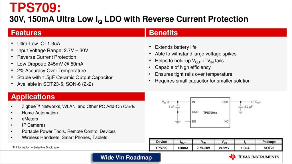
TPS709:30V, 150mA Ultra Low IQ LDO with Reverse Current Protection
Features
Benefits
Ultra-Low IQ: 1.3uA
Input Voltage Range: 2.7V – 30V
Reverse Current Protection
Low Dropout: 245mV @ 50mA
2% Accuracy Over Temperature
Stable with 1.5μF Ceramic Output Capacitor
Available in SOT23-5, SON-6 (2x2)
• Extends battery life
• Able to withstand large voltage spikes
• Helps to hold-up VOUT if VIN fails
• Capable of high efficiency
• Ensures tight rails over temperature
• Requires small capacitor for smaller solution
Applications
Zigbee™ Networks, WLAN, and Other PC Add-On Cards
Home Automation
eMeters
IP Cameras
Portable Power Tools, Remote Control Devices
Wireless Handsets, Smart Phones, Tablets
TI Information – Selective Disclosure
Wide Vin Roadmap
Device
IOUT
VIN
VDO
IQ
Package
TPS709
150mA
2.7V-30V
245mV
1.3uA
SOT23
25. In Development – TLV755: 500mA, Low Vin, LDO Regulator in 1x1mm Package
FeaturesBenefits
Available in 1x1 DFN, SOT23-5, SON-6 2mm x 2mm
Inrush current control
1% Typical Accuracy, 1.5% over Temp
VIN Range: 1.4V-5.5V
Available in fixed voltages: 0.6V to 5.0V
Low IQ: 20uA (typ)
VDO,MAX=220mV @ 500mA (3.3V VOUT)
Foldback Current limit
Available in Active Pulldown
Also available in SOT223 (pin compatible with TLV1117LV)
Applications
Smaller / Cost effective power solution
Eliminate large surge currents during power up.
Stable output for low power applications
Power from wide variety of input rails.
Powers processors with sub 1.0V requirements
Longer battery life
Allows for tighter voltage conversions.
Avoid large fault currents / thermal shutdown
Ensures proper load power cycling.
For best thermal performance.
1.8V
IN
Smartphones/Tablets
Gaming Consoles
Notebooks
Set-top Boxes
Samples:
Available Now
TI Information – Selective Disclosure
CIN
1.5V
OUT
COUT
TLV755
ON
EN
GND
OFF
Device
VIN
IOUT
VDO
IQ
Package
TLV755
1.4V – 5.5V
500mA
220mV@500mA
20uA
1x1 DFN
SOT23-5
2x2 DFN
Low Vin Roadmap
26. In Development – TLV757: 1A, Low Vin, LDO Regulator in 2x2mm Package
FeaturesBenefits
Available in SOT23-5 & 2x2 DFN (DRV)
Inrush current control
1% Typical Accuracy, 1.5% over Temp
VIN Range: 1.6V-5.5V
Available in fixed voltages: 1.0V to 5.0V
Low IQ: 20uA (typ)
VDO,MAX=440mV @ 1A (3.3V VOUT)
Foldback Current limit
Available in Active Pulldown
Also available in SOT223 (pin compatible with TLV1117LV)
Smaller / Cost effective power solution
Eliminate large surge currents during power up.
Stable output for low power applications
Power from wide variety of input rails.
Powers processors with sub 1.0V requirements
Longer battery life
Allows for tighter voltage conversions.
Avoid large fault currents / thermal shutdown
Ensures proper load power cycling.
Applications
1.8V
IN
Smartphones/Tablets
Gaming Consoles
Notebooks
Set-top Boxes
Samples:
Available Now
TI Information – Selective Disclosure
CIN
1.5V
OUT
COUT
TLV757
ON
EN
GND
OFF
Device
VIN
IOUT
VDO
IQ
Package
TLV757
1.6V – 5.5V
1A
440mV@1A
20uA
SOT23-5; 2x2 DFN
SOT223
Low Vin Roadmap
27. In Development – TPS7A05 200mA, Ultra Low IQ LDO in 1x1 package
FeaturesBenefits
• Ultra Low IQ: 1uA (typ); 2uA,max (-40C to +85C)
• 1% Typical Accuracy, 1.5% (-40C to +85C)
• Fast Transient Response
• 1mA to 100mA load: 50us recovery
• Very Low Dropout
• 336mV(max) @ IOUT=200mA,VOUT=1.8V
• Available in fixed output voltages 0.8V to 3.3V
• WCSP (0.65mm X 0.65mm), SON-4 (1x1)
• Available with Active Pulldown (P version)
• TJ = -40 to +125C operation
• Low current for long battery life
• Stable output for low power applications
• Suited for applications with low duty cycles and long sleep
durations
• Allows for maximum efficiency by optimizing upstream power for
minimum power loss.
• Powers processor with sub 1.2V power rails
• Small packaging for space critical applications
• Allows for compliance loads requiring deterministic power down
behavior.
DFN
(SON 4)
Applications
Wearable fitness devices
Tablets, e-readers, Remote Controls
Portable Consumer products
Always-on power supplies
SOT23-5
Device
Samples:
October ‘17
TI Information – Selective Disclosure
WCSP
1mm x 1mm
TPS7A05
VIN
1.4V – 5.5V
IOUT
VDO
200mA
365mV (max)
@VOUT=1.5V
Low Vin Roadmap
IQ
Package
1uA
WCSP (0.35mm pitch)
QFN-4 (1x1); SOT23-5
28. In Development – TPS7A10: Low VIN/Low VOUT, Low IQ 300mA LDO
FeaturesBenefits
VIN Range: 0.7V to 3.6V
VBIAS Range: 1.7V to 5.5V
VOUT Range: 0.5V to 3.3V (fixed)
Ultra Low Dropout: 150mV (max) at 300mA
IQ = 5uA (typ)
PSRR: 40dB @ 1.5MHz
1.0% output accuracy over temp(-40C to 85C)
Active output discharge
Packages available:
• 1.5mmx1.5mm WSON (DSE)
• 0.78mmx1.13mm WCSP-5
• TJ = -40C to 125C
Low VIN operation for optimizing solution efficiency
Allows powering BIAS from as low as 2.5V rail
Low VOUT for support of new ASIC cores.
Allows for minimum power loss at low VIN
Low quiescent current for minimum standby power
Able to reject noise from upstream DC/DC stage
Ideal for rails which require tight regulation.
Ensures well controlled power-down event
Small solution size for space constrained applications.
3.3V
BIAS
1.0V
Applications
Samples: October ‘17
0.8V
TPS7A10
CIN
• Smartphones
• Tablets
• Wearables
TI Information – Selective Disclosure
OUT
IN
ON
COUT
EN
GND
OFF
Device
VIN Range
VBIAS Range
IOUT
IQ
VOUT Range
Max VDO
Package
TPS7A10
0.7V-3.6V
1.7V-5.5V
300mA
5uA
0.5V to 3.3V
150mV @ 300mA
1.5x1.5 DFN
WCSP-5
Low Vin Roadmap
29. In Development – TPS7A25: 18V, 300mA Low IQ LDO with Power Good
FeaturesBenefits
• Low Quiescent Current: 2.5uA
• Input Voltage Range: 2.7V to 18V
• Wide output Range: 1.2V to 17V
• Fixed and Adjustable
• Low Dropout 300mV @ 300mA
• Power Good Output
• 2% Accurate (Max) Fixed and Adj Outputs
• Available in 2x2 DFN and SOT23-6
Applications
Smart Grid and Energy
Building Automation
Portable Industrial Systems
Point of Sale Units
Battery Operated Systems
Samples:
December ‘17
TI Information – Selective Disclosure
Reduces battery drain
Can withstand transients and be used with 12V rails
Generate standard rails: 1.2V, 1.8V, 3.3V, 5V, 12V
Able to provide for very small step-down regulation for
minimum power loss
Allows for monitoring and sequencing of rails
Accurate regulation, fixed outputs for small solution, adjustable
outputs for more flexibility
Available in small solution size or standard easy to use SOT
2.7V – 18V
VIN
PG
EN
VOUT
RPG
CIN
FB
R1
CIOUT = 1uF
R2
GND
Device
Vin Range
Junction Temp
Range
VOUT Range
Max Dropout
Package
TPS7A25
2.7V-18V
-40C to +125C
1.2V to 17V
300mV@300mA
SON-6
SOT-6
Wide Vin Roadmap
30. In Development– TPS746: Adjustable 1A, Low Vin, LDO Regulator with Power Good
FeaturesBenefits
VIN Range: 1.4V-5.5V
Vout: Adjustable and Fixed (0.6V to 5.0V)
1% Typical Accuracy, 2.0% over Temp
High PSRR: 50dB @ 100KHz
Inrush current control
Foldback current limit
Low IQ: 25uA (typ)
Available in Active Pulldown
Power Good Output
Available in 2 x 2 DRV and SOT23-5 (DBV)
Smaller / Cost effective power solution
Eliminate large surge currents during power up
Avoids thermal limit cycling in short circuit faults.
Stable output for low power applications
Power from wide variety of input rails.
Powers processors with sub 1.0V requirements
Longer battery life
Ideal for noise sensitive loads.
Avoid large fault currents / thermal shutdown
Allows sequencing of power rails using the power good signal
Applications
Storage - SSD
Building Automation
Notebooks
Set-top Boxes
Automotive
TI Information – Selective Disclosure
Device
Gainesville2
VIN
1.4V – 5.5V
Low Vin Roadmap
IOUT
1A
VDO
440mV @ 1A
IQ
Package
25uA
2 x2 DFN
SOT23-5
31. In Development – TPS745: Adjustable 500mA, Low Vin, LDO Regulator with Power Good
FeaturesBenefits
VIN Range: 1.4V-5.5V
Vout: Adjustable and Fixed (0.6V to 5.0V)
1% Typical Accuracy, 2.0% over Temp
High PSRR: 50dB @ 100KHz
Inrush current control
Foldback current limit
Low IQ: 25uA (typ)
Available in Active Pulldown
Power Good Output
Available in 2 x 2 DRV and SOT23-5 (DBV)
Smaller / Cost effective power solution
Eliminate large surge currents during power up
Avoids thermal limit cycling in short circuit faults.
Stable output for low power applications
Power from wide variety of input rails.
Powers processors with sub 1.0V requirements
Longer battery life
Ideal for noise sensitive loads.
Avoid large fault currents / thermal shutdown
Allows sequencing of power rails using the power good signal
Applications
Storage - SSD
Building Automation
Notebooks
Set-top Boxes
Automotive
TI Information – Selective Disclosure
Device
Gainesville2
VIN
1.4V – 5.5V
Low Vin Roadmap
IOUT
500mA
VDO
220mV@500mA
IQ
Package
25uA
2 x2 DFN
SOT23-5
32. TLV713P: Capacitor Free, 150mA 1mm x 1mm LDO
FeaturesBenefits
Stable with or without input/output capacitors
Low Vin of 1.4V
Foldback Current Protection
1% Typical Accuracy, 1.5% Accuracy over Temp
Available in fixed voltages 1.0V to 3.3V
TLV713P – Active Output Pulldown
Available in 1x1 SON w/Pad and SOT23-5
Smallest / Cost effective power solution
Increased power supply utilization
Avoid large short currents/ thermal shutdown
Stable output for Low Power App
Powers recent processors with sub <1.2V rail
Quick discharge to control logic
Small solution size
Applications
Wireless Handsets
IP Security Cameras
Smart phones
Tablets
Other Hand-Held Products
TI Information – Selective Disclosure
Device
VIN
IOUT
VDO
IQ
Package
TLV713
1.4 – 5.5
150mA
230mV@
150mA
50uA
SON-4
SOT-23-5
Low Vin Roadmap
33. TLV733 / TLV733P: Capacitor Free, 300mA, Low Vin, LDO Regulator in 1x1mm Package
FeaturesBenefits
Stable with or without an output capacitor
Available in 1x1 DFN and SOT-23-5
Inrush current control
1% Typical Accuracy, 1.25% over Temp
Available in fixed voltages 1.0V to 3.3V
Foldback Current limit
TLV733P – Active output pull-down
Low IQ = 34uA (typ)
Additional voltage options available upon request
Smaller / Cost effective power solution
Eliminate large surge currents during power up
Stable output for low power applications
Powers processors with sub 1.2V requirements
Avoid large fault currents / thermal shutdown
Quick discharge to control logic
Longer battery life
Applications
Wireless Handsets
Smart phones
MP3 Players
Set-top Boxes
Other Hand-Held Products
TI Information – Selective Disclosure
Device
VIN
VOUT
IOUT
VDO
IQ
Package
TLV733P
1.4V – 5.5V
1.0V – 3.3V
300mA
122mV@300mA
34uA
QFN-4,
SOT23-5
Low Vin Roadmap
34. TPS782/3: 150 mA, 500 nA IQ Low Dropout Voltage Regulators
FeaturesBenefits
Ultralow IQ: 500nA (Typ)
Low Dropout: 130 mV
3% Accuracy over Temperature
Stable with 1 uF ceramic capacitor
Active Pulldown (TPS782)
Package: 5SOT (Both) and 6SON (TPS782)
Extended Battery life
Maximize system efficiency
Keeps the rail tight in hot environments
Keeps external component size at minimum
Discharges VOUT while device is off
Minimizes solution size for small applications
Applications
Battery-Powered and Portable Applications
Tablets & Smartphones
Fitness bands
Data logging applications
TI Information – Selective Disclosure
TPS782/3
Device
VIN
VOUT
IOUT
VDO
IQ
Package
TPS782/3
2.2V – 5.5V
1.8V – 4.2V
150mA
130 mV
@ 150mA
500nA
5SOT, 6SON
Low Vin Roadmap
35.
TPS709:30V, 150mA Ultra Low IQ LDO with Reverse Current Protection
Features
Benefits
Ultra-Low IQ: 1.3uA
Input Voltage Range: 2.7V – 30V
Reverse Current Protection
Low Dropout: 245mV @ 50mA
2% Accuracy Over Temperature
Stable with 1.5μF Ceramic Output Capacitor
Available in SOT23-5, SON-6 (2x2)
• Extends battery life
• Able to withstand large voltage spikes
• Helps to hold-up VOUT if VIN fails
• Capable of high efficiency
• Ensures tight rails over temperature
• Requires small capacitor for smaller solution
Applications
Zigbee™ Networks, WLAN, and Other PC Add-On Cards
Home Automation
eMeters
IP Cameras
Portable Power Tools, Remote Control Devices
Wireless Handsets, Smart Phones, Tablets
TI Information – Selective Disclosure
Wide Vin Roadmap
Device
IOUT
VIN
VDO
IQ
Package
TPS709
150mA
2.7V-30V
245mV
1.3uA
SOT23
36. Competitive Database
RESETFilter Priority
Prioritize
Ignore
1
Enter or Select GPN AEC Q100
TI Information – Selective Disclosure
Prioritize Prioritize Prioritize Prioritize Prioritize
Ignore Ignore Ignore Ignore Ignore
3
4
5
6
7
IOUT
(MAX)
[A]
V IN
(MAX)
[V]
V IN
(MIN)
[V]
V OUT
(MAX)
[V]
V OUT
(MIN)
[V]
Prioritize
Ignore
8
Fixed Output
Options [V]
Edit only row 7
Search GPN
Best TI Matches
Competitive Database
Prioritize
Ignore
2
Output Option
Prioritize Prioritize
Ignore Ignore
9
10
Enable
PG
Prioritize
Ignore
11
Prioritize Prioritize Prioritize Prioritize Prioritize Prioritize
Ignore Ignore Ignore Ignore
Ignore
12
13
14
15
16
PSRR @
Output
Noise Accuracy
100KHz
Capacitor Type
[µVrms]
[%]
[dB]
Vdo
(TYP)
[mV]
IQ (TYP)
[mA]
YES
NO
TI Information - Selective Disclosure
LM1085
NO
Adjustable Output,
Fixed Output
3
29
2.6
27.5
1.25
3.3, 5, 12
NO
NO
Non-Ceramic
30
38
1.5
1300
5
TPS7A85A
NO
Adjustable Output,
Programmable Output
4
6.5
1.1
5.1
0.8
ADJ
YES
YES
Ceramic
25
4.4
0.75
150
2.8
LM1084
NO
5.5
29
2.6
27.5
1.25
3.3, 5
NO
NO
Non-Ceramic
30
38
1.6
1300
5
LM338
NO
5
40
4.2
32
1.24
ADJ
NO
NO
Non-Ceramic
10
37
4
2700
0.045
LMS1585A
NO
5
13
2.5
5.75
1.25
1.5, 3.3
NO
NO
Non-Ceramic
-
38
2
1200
LM138
NO
5
40
4.2
32
1.24
ADJ
NO
NO
N/A
-
37
-
3000
-
TPS7A83A
NO
Adjustable Output,
Programmable Output
2
6.5
1.1
5.2
0.8
ADJ
YES
YES
Ceramic
40
4.4
0.75
75
2.8
TLV743P
NO
Fixed Output
0.3
5.5
1.4
3.3
1
1, 1.1, 1.2, 1.5, 1.8,
2.5, 2.8, 2.85, 3, 3.3
YES
NO
Ceramic
28
120
1.4
122
0.034
TLV741P
NO
Fixed Output
0.15
5.5
1.4
3.3
1
1, 1.1, 1.2, 1.5, 1.8,
2.5, 2.8, 2.85, 3, 3.3
YES
NO
Ceramic
17
73
1.5
230
TPS7A92
TPS7A90
NO
NO
6.5
6.5
1.4
1.4
5.2
5.7
0.8
0.8
ADJ
ADJ
YES
YES
YES
YES
Ceramic
Ceramic
48
48
4.7
4.7
1
1
260
75
2.1
2.1
NO
Adjustable Output
Adjustable Output
Adjustable Output,
Fixed Output
2
0.5
LP2951
0.1
30
2
29
1.2
3, 3.3, 5
YES
YES
Non-Ceramic
-
160
2
380
0.075
LM2941
NO
Adjustable Output
1
26
6
20
5
ADJ
YES
NO
Non-Ceramic
67
600
5
500
10
TLV760
LP2950
NO
NO
Fixed Output
Fixed Output
0.1
0.1
30
30
4.2
2
15
5
3.3
3
3.3, 5, 12, 15
3, 3.3, 5
NO
NO
NO
NO
Ceramic
Ceramic
45
-
100
100
4
2
700
110
2
0.075
LM2936
NO
Fixed Output
0.05
60
5.5
5
3
3, 3.3, 5
NO
NO
Non-Ceramic
35
500
3
200
0.015
LM317
NO
Adjustable Output
1.5
40
3
37
1.25
ADJ
NO
NO
Non-Ceramic
38
38
4
2000
3.5
LM317HV
LM117HV
NO
NO
60
60
4.2
4.2
57
57
1.25
1.25
ADJ
ADJ
NO
NO
NO
NO
N/A
N/A
40
-
-
-
2250
1500
-
NO
1
-6
-26
-5
-15
-5, -5.2, -12, -15
NO
NO
Non-Ceramic
23
250
5
600
1
LM337
NO
-40
-1.2
-
1.5
LM137
NO
-40
TPS7A7002
NO
Adjustable Output
Adjustable Output
Fixed Output,
Negative Output
Adjustable Output,
Negative Output
Adjustable Output,
Negative Output
Adjustable Output
1.5
1.5
LM2990
LP38853
NO
Adjustable Output
LP3891
NO
LP3882
NO
TPS7A7001
NO
Adjustable Output
LP3892
NO
Fixed Output
LP38852
NO
Adjustable Output
1.5
Adjustable Output,
Fixed Output
Adjustable Output
Adjustable Output,
Fixed Output
Adjustable Output
-
7
0.05
1.5
-3
-37
ADJ
NO
NO
Non-Ceramic
3
2000
1.5
-4.2
-1.2
-37
ADJ
NO
NO
Non-Ceramic
-
-
-
3000
3
6.5
1.4
5
0.5
ADJ
YES
NO
Ceramic
28
-
2
200
3
3
5.5
1.04
1.8
0.8
ADJ
YES
NO
Ceramic
35
150
3
240
10
Fixed Output
0.8
5.5
1.3
1.8
1.2
1.2, 1.5, 1.8
YES
NO
Non-Ceramic
30
150
2.5
100
4
Fixed Output
1.5
5.5
1.31
1.8
1.2
1.2, 1.5, 1.8
NO
NO
Non-Ceramic
45
90
2.5
110
4
2
6.5
1.4
5
0.5
ADJ
YES
NO
Ceramic
28
-
2
200
1.5
5.5
1.34
1.8
1.2
1.2, 1.5, 1.8
YES
NO
Non-Ceramic
30
150
2.5
140
4
5.5
0.93
1.8
0.8
ADJ
YES
NO
Ceramic
35
90
3
130
10
-
3
36
37. Anpec – APL5930
GPNAEC Q100
TPS7A84A
NO
Adjustable Output,
Output Options
Adjustable Output
Programmable Output
Iout (Max) (A)
3
3
Vin (Max) (V)
3.65
6.5
Vin (Min) (V)
1.2
1.1
Vout (Max) (V)
3.5
5.15
Vout (Min) (V)
0.8
0.8
Fixed Output Options (V)
ADJ
ADJ
Enable
YES
YES
Power Good
YES
YES
Output Capacitor Type
Ceramic
Ceramic
PSRR @ 100KHz (dB)
28
25
Noise (uVrms)
4.4
Accuracy (%)
1.5
0.75
Vdo (Typ) (mV)
230
110
Iq (Typ) (mA)
1
2.8
Thermal Resistance θJA (°C/W)
42
43
Min Package Area (mm2)
19.11
12.25
Package Type
TI Information – Selective Disclosure
APL5930
NO
SOPowerPAD
VQFN
TPS7A84
NO
Adjustable Output,
Programmable Output
3
6.5
1.1
5
0.8
ADJ
YES
YES
Ceramic
25
4.4
1
110
2.8
35
12.25
VQFN
TPS7A7300
TPS7A7002
NO
NO
Adjustable Output,
Adjustable Output
Programmable Output
3
3
6.5
6.5
1.43
1.4
5
5
0.9
0.5
ADJ
ADJ
YES
YES
YES
NO
Ceramic
Ceramic
25
28
40
2
2
240
200
4
3
36
47
25
19.071
VQFN
SOPowerPAD
TPS74901
NO
Adjustable Output
3
5.5
0.8
3.6
0.8
ADJ
YES
YES
Ceramic
28
20
2
120
3
34
9
DDPAK/TO-263,VQFN,VSON
37
38. Diodes – AP7361
TI Information – Selective DisclosureGPN
AEC Q100
AP7361
NO
TPS7A37
NO
TLV1117LV
NO
TPS725
NO
TPS737
NO
Output Options
Adjustable Output,
Fixed Output
Adjustable Output,
Fixed Output
Fixed Output
Iout (Max) (A)
Vin (Max) (V)
Vin (Min) (V)
Vout (Max) (V)
Vout (Min) (V)
1
6
2.2
5
0.8
1
5.5
2.2
5.5
1.2
1
5.5
2
3.3
1.2
1
6
1.8
5.5
1.22
1
5.5
2.2
5.4
1.2
Fixed Output Options (V)
1, 1.2, 1.5, 1.8, 2.5, 2.8,
3.3, ADJ
2.1, 2.5
1.2, 1.5, 1.8, 2.5, 2.8, 3, 3.3
1.5, 1.6, 1.8, 2.5
1.8, 2.5, 3, 3.3, 4
Enable
Power Good
YES
NO
YES
NO
NO
NO
YES
YES
YES
NO
Output Capacitor Type
Ceramic
Ceramic
Ceramic
Cap Free, Ceramic
Ceramic
PSRR @ 100KHz (dB)
Noise (uVrms)
Accuracy (%)
Vdo (Typ) (mV)
Iq (Typ) (mA)
Thermal Resistance θJA (°C/W)
Min Package Area (mm2)
35
1.5
360
0.06
74
9
32
32
1
130
0.4
67
4
50
60
2
570
0.05
63
22.75
20
150
2
170
0.075
23
19.159
33
48
3
130
0.4
50
4
Package Type
WSON, SOPowerPAD,
SOT-223, TO-252, SOT89
WSON
SOT-223
Adjustable Output, Adjustable Output,
Fixed Output
Fixed Output
DDPAK/TOSON,SOT-223,WSON
263,SOIC,SOT-223
38
39. Rohm – BDxxIC0W
GPNAEC Q100
Output Options
Iout (Max) (A)
Vin (Max) (V)
Vin (Min) (V)
Vout (Max) (V)
Vout (Min) (V)
BDxxIC0W
NO
Adjustable Output,
Fixed Output
1
5.5
2.4
4.5
0.8
LP3892
NO
LP3882
NO
LP3879
NO
LP3891
NO
Fixed Output
Fixed Output
Fixed Output
Fixed Output
1.5
5.5
1.34
1.8
1.2
1.5
5.5
1.31
1.8
1.2
0.8
6
2.5
1.2
1
0.8
5.5
1.3
1.8
1.2
Fixed Output Options (V)
1.0, 1.2, 1.25, 1.5, 1.8,
2.5, 2.6, 3.0, 3.3
1.2, 1.5, 1.8
1.2, 1.5, 1.8
1, 1.2
1.2, 1.5, 1.8
Enable
Power Good
Output Capacitor Type
PSRR @ 100KHz (dB)
Noise (uVrms)
Accuracy (%)
Vdo (Typ) (mV)
Iq (Typ) (mA)
Thermal Resistance θJA (°C/W)
Min Package Area (mm2)
YES
NO
Ceramic
1
400
147.1
4.16
YES
NO
Non-Ceramic
30
150
2.5
140
4
40
19.071
NO
NO
Non-Ceramic
45
90
2.5
110
4
40
19.071
YES
NO
Ceramic
35
18
3
475
0.2
40
16
YES
NO
Non-Ceramic
30
150
2.5
100
4
40
19.071
Package Type
SOPowerPAD
TI Information – Selective Disclosure
DDPAK/TO-263,SOPowerPAD DDPAK/TO-263,SOPowerPAD SOPowerPAD,WSON SOPowerPAD,DDPAK/TO-263
39
40. Rohm – BUxxTD2WNVX
GPNAEC Q100
Output Options
Iout (Max) (A)
Vin (Max) (V)
Vin (Min) (V)
Vout (Max) (V)
Vout (Min) (V)
BUxxTD2WNVX
TLV707P
TLV700
TLV705
TPS728
TPS799
NO
NO
NO
NO
NO
NO
Fixed Output
Fixed Output
Fixed Output
Fixed Output
Fixed Output
Adjustable Output, Fixed Output
0.2
0.2
0.2
0.2
0.2
0.2
6
5
5.5
5.5
6.5
6.5
1.7
2
2
2
2.7
2.7
1
3.6
3.6
3.6
3.3
6.5
3.4
1
1.2
1.2
1.2
1.2
1, 1.05, 1.1, 1.15, 1.2,
1, 1.1, 1.2, 1.5, 1.8, 1.2, 1.3, 1.5, 1.8, 1.2, 1.5, 1.8,
1.25, 1.3, 1.5, 1.8, 1.85,
1.2, 1.5, 1.75, 1.8, 1.2, 1.25, 1.3, 1.5, 1.8, 1.85, 1.9,
1.85, 1.9, 2.5, 2.6, 2.8, 1.9, 2.2, 2.5, 2.8, 1.85, 2.5, 2.8,
Fixed Output Options (V) 1.9, 2, 2.05, 2.1, 2.3, 2.5,
1.85, 2.85, 2.95, 3, 1.95, 2, 2.1, 2.5, 2.6, 2.7, 2.75, 2.8,
2.85, 2.9, 3, 3.3, 3.4, 2.9, 3, 3.1, 3.2, 2.85, 3, 3.3, 3.4,
2.6, 2.7, 2.75, 2.8, 2.85,
3.15, 3.3
2.85, 3, 3.15, 3.2, 3.3, 4.2, 4.5
3.6
3.3, 3.6
3.6
2.9, 3, 3.1, 3.2, 3.3, 3.4
Enable
YES
YES
YES
YES
YES
YES
Power Good
NO
NO
NO
NO
NO
NO
Output Capacitor Type
Ceramic
Ceramic
Ceramic
Ceramic
Ceramic
Ceramic
PSRR @ 100KHz (dB)
45
40
51
52
40
38
Noise (uVrms)
45
48
26
210
29
Accuracy (%)
1.5
1.5
2
2
3
2
Vdo (Typ) (mV)
220
250
175
145
230
100
Iq (Typ) (mA)
0.035
0.025
0.03
0.03
0.05
0.04
Thermal Resistance θJA (°C/W)
223
208
236
160
65
74
Min Package Area (mm2)
1
1
2.25
0.5929
1.92
1.92
Package Type
TI Information – Selective Disclosure
X2SON
X2SON
SC70,SOT-23THIN,WSON
DSBGA,DSLGA
DSBGA,WSON
DSBGA,WSON,SOT-23-THIN
40
41. Richtek – RT9069
GPNAEC Q100
RT9069
NO
LM340
NO
TLV760
NO
TPS709
NO
TLV704
NO
Output Options
Fixed Output
Fixed Output
Fixed Output
Fixed Output
Fixed Output
Iout (Max) (A)
Vin (Max) (V)
Vin (Min) (V)
Vout (Max) (V)
Vout (Min) (V)
0.2
36
3.5
12
2.5
1.5
35
7.5
15
5
0.1
30
4.2
15
3.3
0.15
30
2.7
6
1.2
0.15
24
2.5
5
3
Fixed Output Options (V)
2.5, 3, 3.3, 5, 9, 12
5, 12, 15
3.3, 5, 12, 15
1.2, 1.35, 1.5, 1.6, 1.8, 1.9, 2.5,
2.7, 2.8, 3, 3.3, 3.6, 3.8, 3.9, 5, 6
3, 3.3, 3.6, 5
Enable
Power Good
YES
NO
NO
NO
NO
NO
YES
NO
NO
NO
Output Capacitor Type
Ceramic
Cap Free, Ceramic
Ceramic
Ceramic
Ceramic
PSRR @ 100KHz (dB)
Noise (uVrms)
Accuracy (%)
Vdo (Typ) (mV)
Iq (Typ) (mA)
Thermal Resistance θJA (°C/W)
Min Package Area (mm2)
40
2
200
0.0035
30.6
2.56
50
40
5
2000
8
24
22.75
45
100
4
700
2
270
4.64
26
190
2
300
0.001
73
4
42
550
2
400
0.003
213
4.64
SOT-23
SOT-23,WSON
SOT-23
Package Type
TI Information – Selective Disclosure
SOPowerPAD, SOT-89, SOT-23, DDPAK/TO-263,TO-3,SOTSON
223,TO-220
41
42. Rohm – BUxxUA3
GPNAEC Q100
BUxxUA3WNVX
NO
TLV733P
NO
LP5907
NO
LP5910
NO
TLV702
NO
Output Options
Fixed Output
Fixed Output
Fixed Output
Fixed Output
Fixed Output
Iout (Max) (A)
Vin (Max) (V)
Vin (Min) (V)
Vout (Max) (V)
Vout (Min) (V)
0.3
5.5
1.4
3.3
1
0.25
5.5
2.2
4.5
1.2
0.3
3.3
1.3
1.8
0.9
0.3
5.5
2
4.75
1.2
Enable
Power Good
Output Capacitor Type
PSRR @ 100KHz (dB)
Noise (uVrms)
Accuracy (%)
Vdo (Typ) (mV)
Iq (Typ) (mA)
Thermal Resistance θJA (°C/W)
Min Package Area (mm2)
0.3
5.5
1.7
4
1
1, 1.05, 1.1, 1.15, 1.2, 1.25, 1.3, 1.35, 1.4,
1.45, 1.5, 1.55, 1.6, 1.65, 1.7, 1.75, 1.8, 1.85,
.19, 1.95, 2, 2.05, 2.1, 2.15, 2.2, 2.25, 2.3,
2.35, 2.4, 2.45, 2.5, 2.55, 2.6, 2.65, 2.7, 2.75,
2.8, 2.85, 2.9, 2.95, 3, 3.05, 3.1, 3.15, 3.2,
3.25, 3.3, 3.35, 3.4, 3.45, 3.5, 3.55, 3.6, 3.65,
3.7, 3.5, 3.8, 3.85, 3.9, 3.95, 4
YES
NO
Ceramic
30
1
200
0.05
223
1
Package Type
X2SON
Fixed Output Options (V)
TI Information – Selective Disclosure
1.2, 1.5, 1.8, 1.9,
1.2, 1.5, 1.8, 2.5,
1, 1.1, 1.2, 1.5, 1.8, 2.2, 2.5, 2.7, 2.75,
2.8, 2.9, 3, 3.1,
0.9, 1, 1.1, 1.2, 1.8
2.5, 2.8, 2.85, 3, 3.3 2.8, 2.85, 2.9, 3, 3.1,
3.3, 3.5, 3.6, 3.7,
3.2, 3.3, 3.7, 4, 4.5
4.3, 4.5, 4.75
YES
NO
Cap Free, Ceramic
28
120
1.4
122
0.034
219
1
YES
NO
Ceramic
60
6.5
2
50
0.012
193
0.77
YES
NO
Ceramic
40
12
2
120
0.012
79
0.49
YES
NO
Ceramic
51
48
2
220
0.03
249
2.25
SOT-23,X2SON
SOT23,X2SON,DSBGA
DSBGA,WSON
SOT-23,WSON
42
43. Intersil – ISL9021A
ISL9021ATLV733P
LP5910
TPS720
VIN (V)
1.5 to 5.5
1.4 to 5.5
1.3 to 3.3
1.1 to 4.5
VOUT (V)
Fixed/Adj
IOUT (mA)
Current Limit (min) (mA)
0.9 to 3.3
Fixed
250
260
1 to 3.3
Fixed
300
360
0.9 to 1.8
Fixed
300
450 (typ)
0.9 to 1.8
Fixed
350
420
FB/VOUT Accuracy (max)
1.8%
1.4% (over temp)
2%
2%
IQ (no load) (max) (μA)
IQ (shutdown) (μA)
Noise
(10Hz to 100kHz) (μVRMS)
50
1
60
1 (@25°C)
25
2
30 (typ), 80
2
8.5 x VOUT
66 x VOUT
12
32 x VOUT
0.975x1.155 WCSP
1.6x1.6 DFN-6
1x1 X2SON
SOT23-5
0.75x0.75 WCSP
2.1x2.1 DFN-6
1.36x0.96 WCSP
2x2 DFN-6
250
250
150
142
135.64
-40 to 85°C
Y
N
1
218.6
-40 to 125°C
Y
Y
0
79.2
-40 to 125°C
Y
N
1
66.5
-40 to 125°C
Y
N
2.2
Package
Dropout (VDO) (max)
(250mA) (mV)
θJA (°C/W)
Temp Range
Enable (EN)?
Cap-Free?
COUT (min) (μF)
TI Information – Selective Disclosure
43
44. Ricoh – RP114
RP114xTLV733P
LP5910
TLV702
VIN (V)
1.4 to 5.5
1.4 to 5.5
1.3 to 3.3
2 to 5.5
VOUT (V)
Fixed/Adj
IOUT (mA)
Current Limit (min) (mA)
0.8 to 3.6
Fixed
300
300
1 to 3.3
Fixed
300
360
0.8 to 2.3
Fixed
300
450 (typ)
1.2 to 4.75
Fixed
300
320
FB/VOUT Accuracy (max)
3% (over temp)
1.4% (over temp)
2%
2% (over temp)
IQ (no load) (max) (μA)
IQ (shutdown) (μA)
75
1 (@25°C)
1x1 X2SON
SC70-5
SOT23-5
390 (@1.8V)
290 (@3.3V)
250
-40 to 85°C
Y
N
60
1 (@25°C)
25
2
55
2
1x1 X2SON
SOT23-5
0.75x0.75 WCSP
2.1x2.1 DFN-6
SOT23-5
1.5x1.5 DFN-6
180 (@1.8V)
375
79.2
-40 to 125°C
Y
N
249.2
-40 to 125°C
Y
N
Package
Dropout (VDO) (max)
(300mA) (mV)
θJA (°C/W)
Temp Range
Enable (EN)?
Cap-Free?
TI Information – Selective Disclosure
300 (@1.8V)
270 (@3.3V)
218.6
-40 to 125°C
Y
Y
44
45. Ricoh – RP103
RP103TLV733
TLV707
TLV702
VIN (V)
1.7 to 5.25
1.4 to 5.5
2 to 5
2 to 5.5
VOUT (V)
Fixed/Adj
IOUT (mA)
Current Limit (min) (mA)
FB/VOUT Accuracy (max)
IQ (no load) (max) (μA)
IQ (shutdown) (μA)
1.2 to 3.3
Fixed
150
180
1.5% (over temp)
50
1 @ 25°C
1x1 X2SON-4
SC70-4
SOT23-5
1 to 3.3
Fixed
300
360
1.4% (over temp)
60
1 @ 25°C
0.85 to 3.6
Fixed
200
240
1.5% (over temp)
50
1 @ 25°C (typ)
1.2 to 4.75
Fixed
300
320
2% (over temp)
55
2
1x1 X2SON-4
SOT23-5
1x1 X2SON-4
1.5x1.5 DFN-6
SOT23-5
Dropout (VDO) (max)
(150mA) (mV)
270 (3.3V)
270 (3.3V)
270 (3.3V)
188
Noise
(10Hz – 100kHz) (μVRMS)
50 x VOUT
66 x VOUT
25 x VOUT
27 x VOUT
θJA (°C/W)
250
218.6
208.1
249.2
Enable (EN)?
Cap-Free?
Output Cap (min) (μF)
Temp Range
Y
N
0.47
-40 to 85°C
Y
Y
0
-40 to 125°C
Y
N
0.1
-40 to 125°C
Y
N
0.1
-40 to 125°C
Package
TI Information – Selective Disclosure
45
46. Torex – XC6209, XC6212
XC6209/12TLV713P
TPS709
TLV704
VIN (V)
2 to 10
1.4 to 5.5
2.7 to 30
2.5 to 24
VOUT (V)
Fixed/Adj
IOUT (mA)
Current Limit (min) (mA)
0.9 to 6
Fixed
150
300 (typ)
1 to 3.3
Fixed
150
180
1.5 to 6
Fixed
150
200
3 to 5
Fixed
150
160
FB/VOUT Accuracy (max)
2% (25°C)
1.5%
2% (over temp)
2% (25°C)
IQ (no load) (max) (μA)
IQ (shutdown) (μA)
50 (25°C)
0.1 (typ)
SOT23-5
1.8x2 DFN-6
SOT89-5
75
1
2.05
0.15 (typ)
4.5 (25°C)
-
SOT23-5
1x1 X2SON
SOT23-5
2x2 SON-6
SOT23-5
410
600
1200
1650 (25°C)
100
-40 to 85°C
Y
N
249
-40 to 125°C
Y
Y
73.1
-40 to 125°C
Y
N
213.1
-40 to 125°C
N
N
Package
Dropout (VDO) (max)
(@150mA) (mV)
θJA (°C/W)
Temp Range
Enable (EN)?
Cap-Free?
TI Information – Selective Disclosure
46
47. Analog Devices – ADP150, ADP151
ADP1502.2 to 5
1.8 to 3.3
Fixed
150
ADP151
2.2 to 5
1.1 to 3.3
Fixed
200
LP5907
2.2 to 5.5
1.2 to 4.5
Fixed
250
TLV707
2 to 5
0.85 to 3.6
Fixed
200
160
150
120
225
FB/VOUT Accuracy (max)
-2.5/+1.5
-2.5/+1.5
2
1.5
IQ (no load) (max) (μA)
IQ (shutdown) (μA)
Noise
(10Hz – 100kHz) (μVRMS)
(10kHz)
(100kHz)
PSRR (dB)
(500kHz)
(1MHz)
(2MHz)
θJA (°C/W)
Output Discharge?
Enable (EN)?
22
1
20
1
25
1
50
1 (typ)
9
9
6.5
25 x VOUT
59
48
36
33
37
170
N
Y
57
46
39
32
33
63.6
N
Y
0.8x0.8 WCSP
2x2 DFN-6
SOT23-5
69
63
47
38
32
193.4
Y
Y
0.65x0.65 WCSP
1x1 X2SON
SOT23-5
50
40
43
47
48
208.1
Y
Y
VIN (V)
VOUT (V)
Fixed/Adj
IOUT (mA)
Dropout (VDO) (@150mA)
(mV)
Package
TI Information – Selective Disclosure
0.8x0.8 WCSP
SOT23-5
1x1 X2SON
47
48. Linear Tech – LT1761, LT1962
LT1761LT1962
TPS7A49
LP5907
VIN (V)
1.8 to 20
1.8 to 20
3 to 36
2.2 to 5
VOUT (V)
1.22 to 20 (adj.)
1.2 to 5 (fixed)
1.22 to 20 (adj.)
1.5 to 5 (fixed)
1.2 to 33 (adj.)
1.2 to 4.5 (fixed)
IOUT (max) (mA)
100mA
300mA
150mA
250mA
30 x VOUT
33 x VOUT
12.8 x VOUT
6.5
450
330
400
100
30
35
55
60
20uA
30uA
>60uA
12uA
θJA (°C/W)
125
110
47.7
193.4
Soft Start?
No
No
Yes
No
Package
2.8x2.9mm 5SOT-23
3x5mm MSOP-8
3x3mm DFN
3x5mm MSOP-8 PowerPad
2.8x2.9mm 5SOT-23
1x1mm QFN
Noise
(10Hz to 100kHz)
(μVRMS)
VDO (max)
(@100mA) (mV)
PSRR (100kHz)
(dB)
Quiescent
current (IQ) (μA)
TI Information – Selective Disclosure
48
49. Diodes – AP7361
AP73612.2 to 6
1 to 5
1
90 (@25°C)
TPS7A37
2.2 to 5.5
1.2 to 5.5
1
400
TLV1117LV
2 to 5.5
1.2 to 3.3
1
100 (@25°C)
0.7 (@25°C)
0.2
0.7 (@25°C)
FB/VOUT Accuracy (max)
3
1
2 (@25°C)
PSRR (100kHz) (dB)
Noise
(10Hz – 100kHz) (μVRMS)
28
33
50
-
27 x VOUT
33 x VOUT
2x2 DFN
SOT223-4
1
N
Y
Y
-40 to 125°C
1
N
N
N
-40 to 125°C
VIN (V)
VOUT (V)
IOUT (A)
IQ (no load) (max) (μA)
Dropout (VDO) (max)
(@1A) (V)
Package
COUT (min) (μF)
Soft Start?
Enable?
Reverse Current Protection?
Temp Range
TI Information – Selective Disclosure
3x3 DFN-8
SOT223-4
TO252-3
SOT89-5
SO-8
2.2
N
Y
N
-40 to 85°C
49
50. Richtek – RT9059
VIN (V)VOUT (V)
VBIAS?
Fixed/Adj
IOUT (A)
Dropout (VDO) (max)
(@3A) (mV)
FB/VOUT Accuracy (max)
Noise
(10Hz – 100kHz) (μVRMS)
PSRR (100kHz) (dB)
PSRR (1MHz) (dB)
Package
Enable (EN)?
NR/SS?
Power Good (PG)?
θJA (°C/W)
TI Information – Selective Disclosure
RT9059
1 to 5
0.8 to (VIN - VDO)
Y
Adj.
3
TPS7A84
1.1 to 6.5
0.8 to 5
Optional
Adj.
3
TPS74401
0.9 to 5.5
0.9 to 3.6
Y
Adj.
3
TPS74901
0.9 to 5.5
0.8 to 3.6
Y
Adj.
3
450 @ 25°C
180
195
280
1.5% @ 25°C + resistor
tolerance
1%
1% + resistor tolerance
2% + resistor tolerance
N/A
5.5 x VOUT
16 x VOUT
25 x VOUT
N/A
N/A
3x3 DFN-10
SO-8
Y
N
Y
70
19
30
27
27
12
22
3.5x3.5 QFN-20
5x5 QFN-20
3x3 DFN-10
Y
Y
Y
35.4
Y
Y
Y
35.4
Y
Y
Y
48.1
50