 electronics
Similar presentations:
")

")


The largest complex in Russia for conducting scientific and technological research in the field of micro- and nanoelectronics
1.
Research Institute of Molecular Electronics (MERI)The largest complex in Russia for conducting scientific and technological research in the
field of micro- and nanoelectronics
2.
About Our CompanyJSC Research Institute of Molecular Electronics is a company responsible for the
implementation of the priority technological area “Electronic Technologies” of the
Russian Federation (Order of the Government of the Russian Federation of 20.09.2016
No. 1984-r)
The number of R&D center staff exceeds
600 engineers and scientists
3 Academicians of RAS, 2 Corresponding
Members of RAS
Over 70 Ph.D. and D.Sc.
25 laureates of State Prizes of the Russian
Federation and Prizes of the Government of
Russia in the field of science and technology
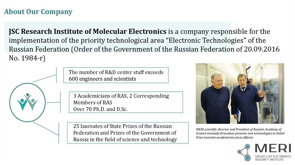
MERI scientific director and President of Russian Academy of
Science Gennady Krasnikov presents new technologies to Nobel
Prize laureate academician Jores Alferov
3.
MERI: Success StoriesIn 2008 the general director of
MERI,
Academician
Gennady
Krasnikov joined the Board of
directors
of
the
Global
Semiconductor
Alliance
from
Europe, Middle East and Africa
(EMEA Leadership Council GSA).
In 2016 in Paris the general
director of MERI JSC, RAS
Academician Gennady Krasnikov
was awarded the UNESCO medal
“For
Contribution
to
the
Development of Nanoscience and
Nanotechnology”.
In 2017 MERI became a full
member of GSA - The Global
Semiconductor Alliance.
In addition to this, MERI has
successfully
completed
international joint projects of
technology transfer with ST
Microelectronics, Infineon and
Giesecke &Devrient.
In 2012 developed by MERI eIDmicrochip with banking application
had received EMVCo certification and
became
the
6-th
worldwide
microchip
authorized
by
VISA/MasterCard for use in their
process payment system.
In 2018 and 2019 MERI was
consistently rated as a leader of
Russian radio-electronic industry in
terms of revenue from its scientific
and research activities.
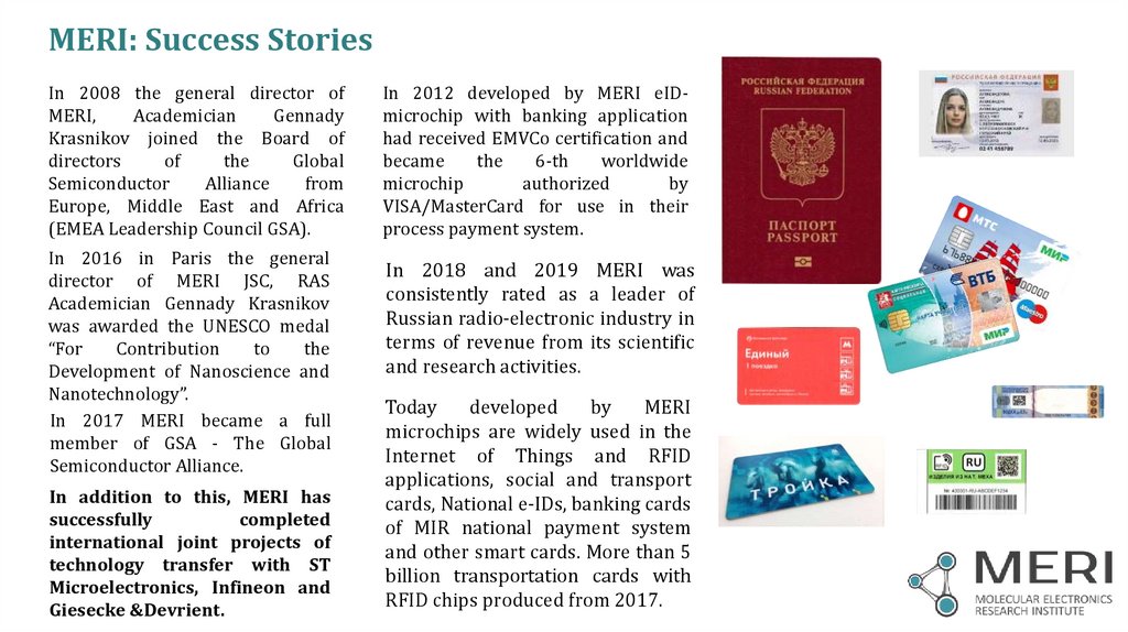
Today
developed
by
MERI
microchips are widely used in the
Internet of Things and RFID
applications, social and transport
cards, National e-IDs, banking cards
of MIR national payment system
and other smart cards. More than 5
billion transportation cards with
RFID chips produced from 2017.
4.
General information for project in IndiaMERI is ready to act as a technological supplier of technology for the transfer of
the design technology and 180 nm chips manufacture*.
(*For more details please check the Appendixes to the current presentation)
In case of agreement between the parties, a project office consisting of MERI’s
specialists will be formed to consult on a regular basis for the following points:
- technology selection
- tools selection
- list of tools
- infrastructure requirements
- trainings for engineers
To be paid upon
actual costs
MERI representatives are ready to travel to India for a study visit and presentation
of MERI.
5.
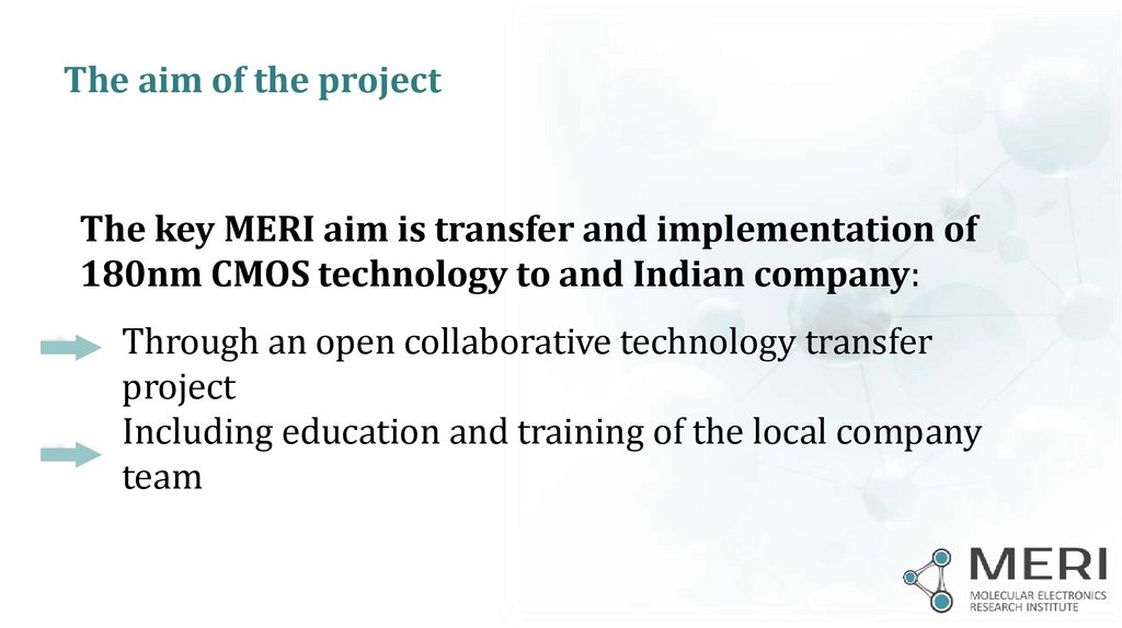
The aim of the projectThe key MERI aim is transfer and implementation of
180nm CMOS technology to and Indian company:
Through an open collaborative technology transfer
project
To be paid
upon
Including
education and training of the local company
actual costs
team
6.
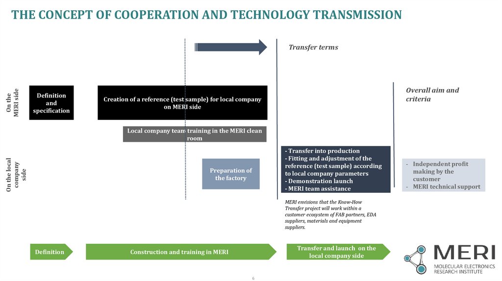
THE CONCEPT OF COOPERATION AND TECHNOLOGY TRANSMISSIONOn the
MERI side
Transfer terms
Definition
and
specification
Overall aim and
criteria
Creation of a reference (test sample) for local company
on MERI side
On the local
company
side
Local company team training in the MERI clean
room
- Transfer into production
- Fitting and adjustment of the
reference (test sample) according
to local company parameters
- Demonstration launch
- MERI team assistance
Preparation of
the factory
MERI envisions that the Know-How
Transfer project will work within a
customer ecosystem of FAB partners, EDA
suppliers, materials and equipment
suppliers.
Definition
Transfer and launch on the
local company side
Construction and training in MERI
6
- Independent profit
making by the
customer
- MERI technical support
7.
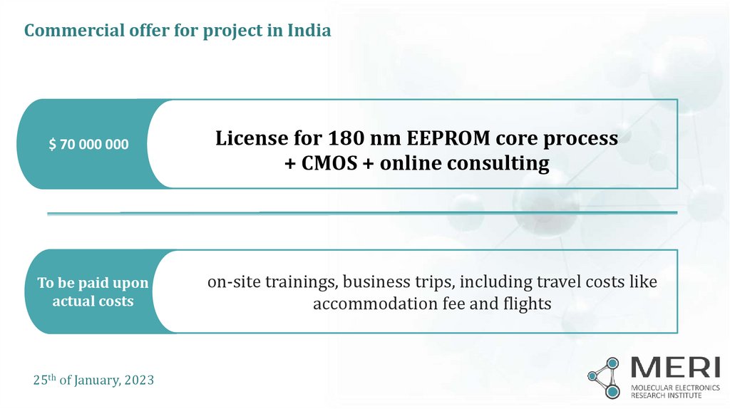
Commercial offer for project in India$ 70 000 000
To be paid upon
actual costs
25th of January, 2023
License for 180 nm EEPROM core process
+ CMOS + online consulting
on-site trainings, business trips, including travel costs like
accommodation fee and flights
8.
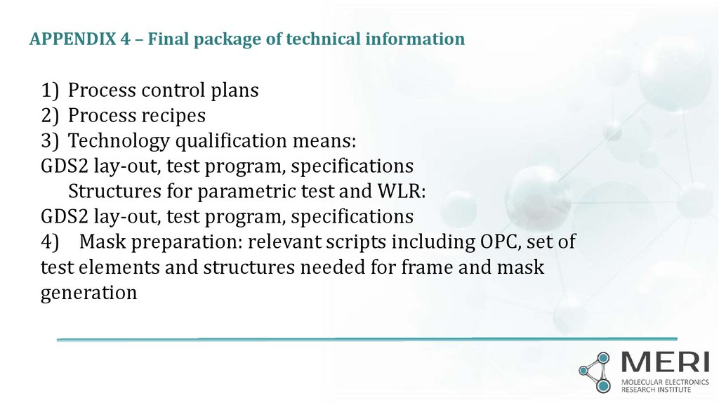
APPENDIX 4 – Final package of technical information1) Process control plans
2) Process recipes
3) Technology qualification means:
GDS2 lay-out, test program, specifications
Structures for parametric test and WLR:
GDS2 lay-out, test program, specifications
4) Mask preparation: relevant scripts including OPC, set of
test elements and structures needed for frame and mask
To be paid upon
generation
actual costs
9.
APPENDIX 1 - General process information about technologyPROCESS KEY POINTS
Power supply: this process is designed for 1.8 V applications (± 0.15V) with 5V Capable
I/O's.
Front-end main features: Shallow trench isolation, twin-tub CMOS process using a type
P/P+ epi substrate (epi thickness = 6mm (*), p resistivity = 10-13 Om cm).
This process features salicide on junctions and poly, and resistors on active and
interconnect N+ or P+ poly, with dedicated process modules to integrate HV transistors for
EEPROM operation. Low Leakage transistors (with High Vt) are available for 1.8 V
applications.
Back-end main features: Damascene Local Interconnect Level (LIL) for short interconnects;
tungsten material (R=320 mOhm/sq). Metal 1, 2, 3, 4: 0.64 µm pitch, Al-Cu levels for routing
(R=72 mOhm/sq). Metal 5 for shield (special option for Smart-Card): 0.64 µm pitch, Al-Cu
metal layer (same as Metal 4) only for shield in Smart-Card devices, allowing dense routing
To
be4ML.
paidMetal
upon5, 6 (not available for Smart-Card applications): 1.28µm pitch, preferred
with
actual
layers
for costs
power, clock, busses and major interconnect signal distribution (R=35
mOhm/sq). Low K dielectrics as intralevel dielectric for Metal 1, 2, 3, 4.
10.
APPENDIX 2 – Initial package of technical information (PROCESS)1) Process Flow of the Technology
2) List of Process/Control/Measurement/Characterization
tools specific to the Technology
3) Specifications for gases, chemicals, materials, utilities is
specific to the Technology
4) Technical equipment procurement specifications to be
used for tool procurement from Suppliers
To be paid upon
actual costs
11.
APPENDIX 3 – Initial package of technical information (DESIGN)1) Design flow with cad and internal software specification used on
each step
2) List of CAD tools and softwares used in the design flow and in
memory compilers, with relevant information about Version,
Suppliers
3) Design rules manual (DRM)
4) Process design kits and libraries and IP’s for technology, with
detailed information
5) Memory compilers with relevant licenses to be procured by
Customer
6)beMask
preparation: list of software tools, requirements for hardware
To
paid upon
actual
and costs
software environment, process control structures for mask
manufacturing at Maskshops DNP/DPE
12.
6/1 Akademika Valieva street,Zelenograd, Moscow
124460, Russia
Tel. +7 (495) 229-70-00
www.niime.ru/en