Similar presentations:
Topology Swapping for Switchers - Sanjaya Maniktala
1. Topology Swapping for Switchers - Sanjaya Maniktala
for :Switching Power Supplies A to Z
2. A Switcher is a Switcher is a Switcher
A switcher IC is basically this:• A switch (Fet or Bipolar)
• A diode (for freewheeling and transferring
energy to the output)
• An inductor for energy storage during the
process
• Input and Output Capacitors
Sanjaya Maniktala: “Topology Swapping”
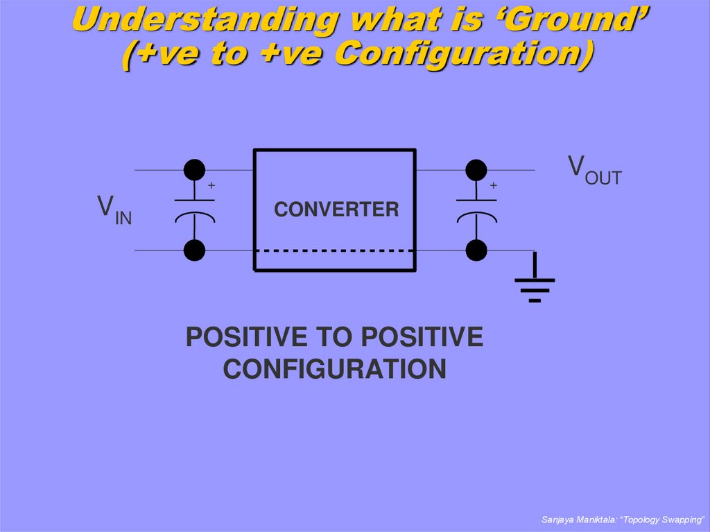
3. Understanding what is ‘Ground’ (+ve to +ve Configuration)
+VIN
+
VOUT
CONVERTER
POSITIVE TO POSITIVE
CONFIGURATION
Sanjaya Maniktala: “Topology Swapping”
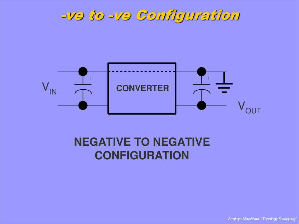
4. -ve to -ve Configuration
+VIN
+
CONVERTER
VOUT
NEGATIVE TO NEGATIVE
CONFIGURATION
Sanjaya Maniktala: “Topology Swapping”
5. -ve to +ve Configuration
+VIN
+
VOUT
CONVERTER
NEGATIVE TO POSITIVE
CONFIGURATION
Sanjaya Maniktala: “Topology Swapping”
6. +ve to -ve Configuration
+VIN
+
CONVERTER
VOUT
POSITIVE TO NEGATIVE
CONFIGURATION
Sanjaya Maniktala: “Topology Swapping”
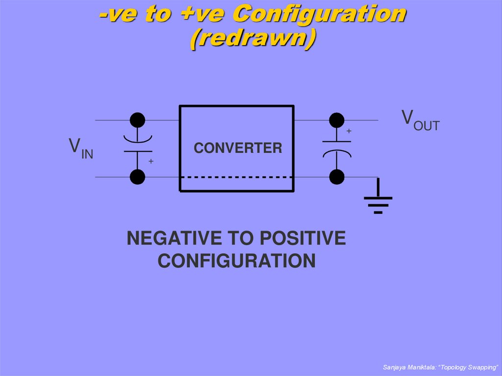
7. -ve to +ve Configuration (redrawn)
+VIN
VOUT
CONVERTER
+
NEGATIVE TO POSITIVE
CONFIGURATION
Sanjaya Maniktala: “Topology Swapping”
8. +ve to -ve Configuration (redrawn)
VOUT+
VIN
CONVERTER
+
POSITIVE TO NEGATIVE
CONFIGURATION
Sanjaya Maniktala: “Topology Swapping”
9. What about the IC Ground?
In fact there are so many definitions of‘Ground’ that it does become confusing. For
example we also have the IC (or ‘control’)
Ground (sometimes called the ‘analog’
Ground).
In particular, the IC Ground may NOT be the
same as the power ground!!
Sanjaya Maniktala: “Topology Swapping”
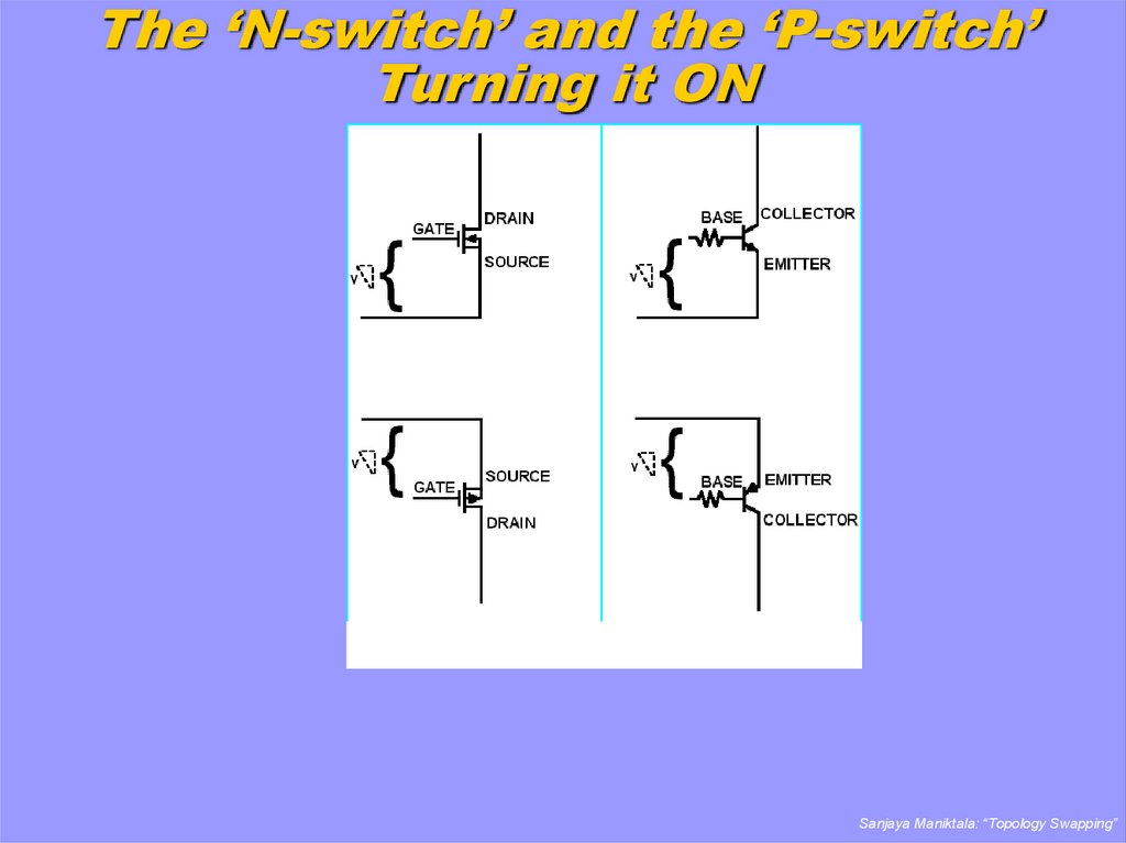
10. The ‘N-switch’ and the ‘P-switch’ Turning it ON
Sanjaya Maniktala: “Topology Swapping”11. The ‘N-switch’ and the ‘P-switch’ Turning it OFF
Sanjaya Maniktala: “Topology Swapping”12. The ‘LSD’ Cell
Sanjaya Maniktala: “Topology Swapping”13. The terminology
If the cathode of the diode connects to the LSD node: call it a ‘+’
LSD cell
If the anode of the diode connects to the LSD node: call it a ‘-’
LSD cell
So,
1.
Type A: N+ cell: cathode is LSD node, N-channel
FET or NPN BJT
2. Type B :N- cell: anode is LSD node, N-channel FET
or NPN BJT
3.
Type C : P- cell: anode is LSD node, P-channel
FET or PNP BJT
4.
Type D : P+ cell: cathode is LSD node, P-channel
FET or PNP BJT
Sanjaya Maniktala: “Topology Swapping”
14. Lookup Table for LSD Descriptors
Sanjaya Maniktala: “Topology Swapping”15. What are configurations?
• The words ‘step-down’ (Buck) or ‘step-up’(Boost) or ‘step up/down’ (Buck-Boost)
merely refer to the MAGNITUDES of the
input and output voltages. These are
therefore TOPOLOGIES.
• But we can have for example a +ve to +ve
Buck or –ve to –ve Buck. So the qualifiers
are the CONFIGURATIONS
Sanjaya Maniktala: “Topology Swapping”
16. Buck-Boost Configurations
• The Buck-Boost will take a given voltage and changeit to either a smaller voltage (Buck) or a larger
voltage (Boost) depending on the duty cycle.
• However it can be shown that in the process, the
polarity is ALWAYS inverted.
• A topology which can change say +10V to +15V and
also do +10V to +5V (at our will) does NOT exist.
• A topology which will invert polarities but just be
capable of Bucking or only Boosting, also does not
exist.
Sanjaya Maniktala: “Topology Swapping”
17. Buck Configurations
Sanjaya Maniktala: “Topology Swapping”18. Boost Configurations
Sanjaya Maniktala: “Topology Swapping”19. Buck-Boost Configurations
Sanjaya Maniktala: “Topology Swapping”20. N-Switch Configurations to P-Switch Configurations
To draw the negative ground circuit from apositive ground circuit (and vice versa) we
simply invert all circuit polarities.
Sanjaya Maniktala: “Topology Swapping”
21. ‘Inversion’
Sanjaya Maniktala: “Topology Swapping”22. An example of ‘Inversion’
Sanjaya Maniktala: “Topology Swapping”23. Why study the IC Construction?
Having understood the topologies and theirconfigurations, it is important to also note
the internal construction of the switcher IC,
so that we can tap its full potential and judge
its suitability for a particular
topology/configuration.
Sanjaya Maniktala: “Topology Swapping”
24. Type 1 IC (“Boost/Buck-Boost IC”)
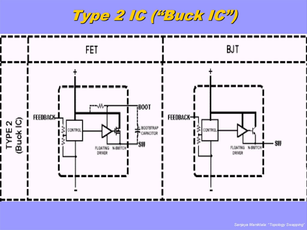
Sanjaya Maniktala: “Topology Swapping”25. Type 2 IC (“Buck IC”)
Sanjaya Maniktala: “Topology Swapping”26. Summary of IC differences (1)
• Type 1 connects the Source/Emitter (lowervoltage switch pin) to the - pin of the control
block.
• Type 2 connects the Drain/Collector (higher
voltage switch pin) to the + pin of the control
block.
Sanjaya Maniktala: “Topology Swapping”
27. Summary of IC differences (2)
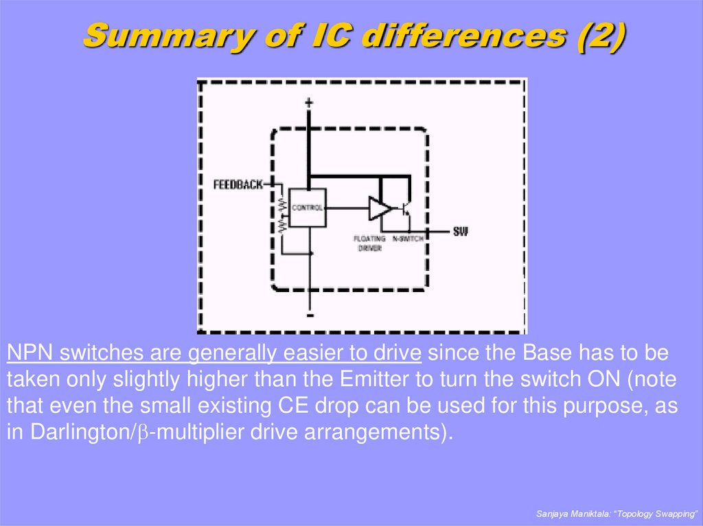
NPN switches are generally easier to drive since the Base has to betaken only slightly higher than the Emitter to turn the switch ON (note
that even the small existing CE drop can be used for this purpose, as
in Darlington/ -multiplier drive arrangements).
Sanjaya Maniktala: “Topology Swapping”
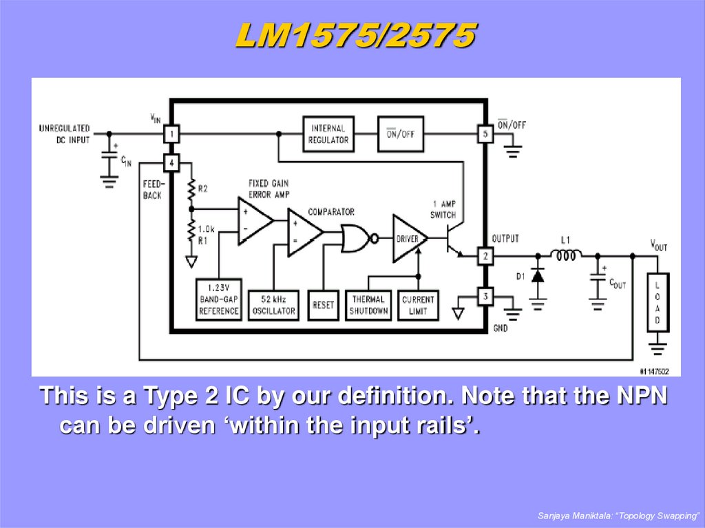
28. LM1575/2575
This is a Type 2 IC by our definition. Note that the NPNcan be driven ‘within the input rails’.
Sanjaya Maniktala: “Topology Swapping”
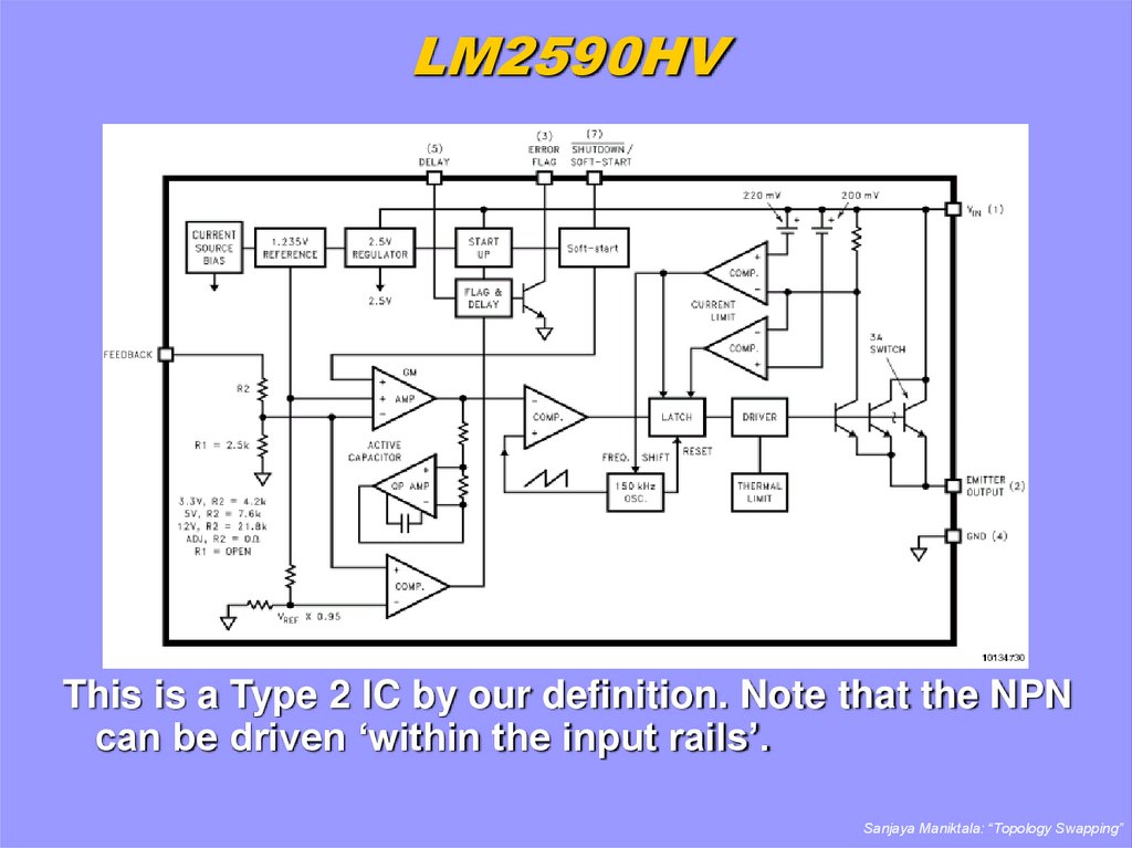
29. LM2590HV
This is a Type 2 IC by our definition. Note that the NPNcan be driven ‘within the input rails’.
Sanjaya Maniktala: “Topology Swapping”
30. Type 2 IC’s with NPN Switches
• We see that the ‘drop’ across the switch isuniformly high, almost irrespective of load
current rating. It is always about 1.4V (worst
case over temperature). You need this drop
to be able to drive the Switch ON (and keep
it ON). The only way to reduce this drop is to
go to Type 2 IC’s which use an N-Fet.
Sanjaya Maniktala: “Topology Swapping”
31. LM2670
This is a Type 2 IC by our definition. Note that the NFet has to be driven ‘outside the input rails’.Sanjaya Maniktala: “Topology Swapping”
32. Summary of IC differences (3)
• Returning to N-switches, we can conclude thatdespite their advantages, the drive of FET-based
Type 2 ICs are the the most complex. We must
recognize that when the switch turns ON, the
Source/Emitter pin becomes (almost) equal to the ‘+’
supply pin. But to keep the FET ON, a voltage higher
than the IC supply pin is required (typically 5-10
Volts higher depending on type of FET). This is not
readily available as it is outside the range of the
input supply rails. In fact there is no other easy way
other than to bootstrap the driver stage, such that
the driver floats on the switching node.
Sanjaya Maniktala: “Topology Swapping”
33. A ‘Boost IC’: the LM2577
• This is a Boost application. So can IC this do BuckBoost/Flyback????Sanjaya Maniktala: “Topology Swapping”
34. LM2577 as a Flyback
• So why wasn’t this obvious right away???Sanjaya Maniktala: “Topology Swapping”
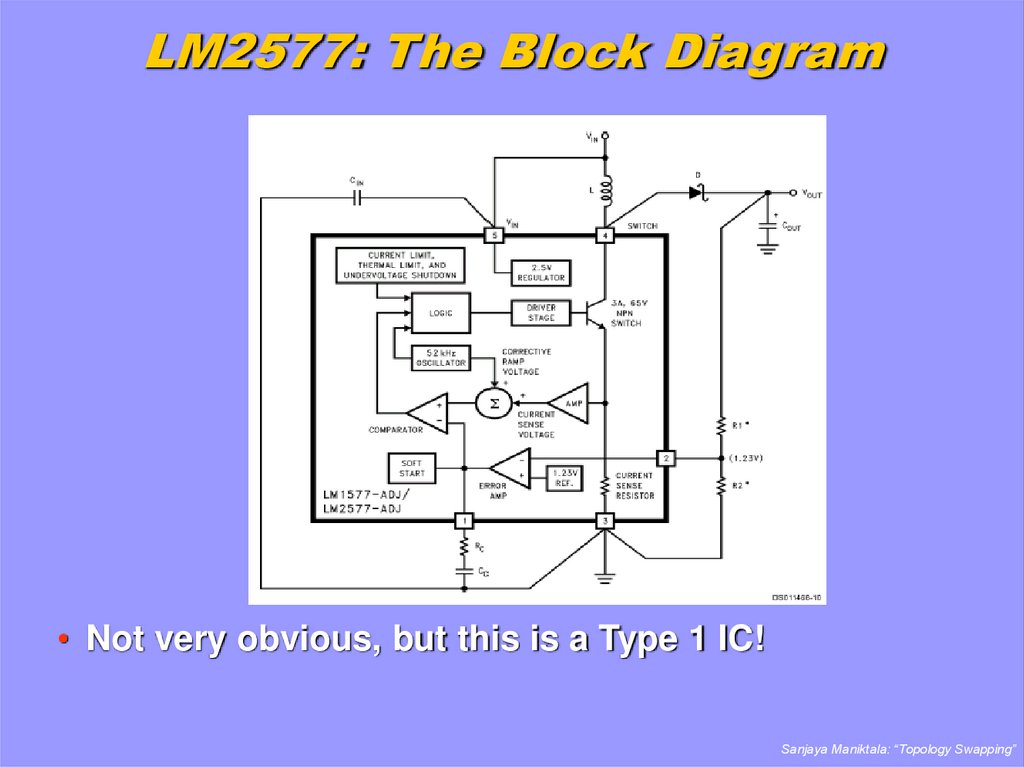
35. LM2577: The Block Diagram
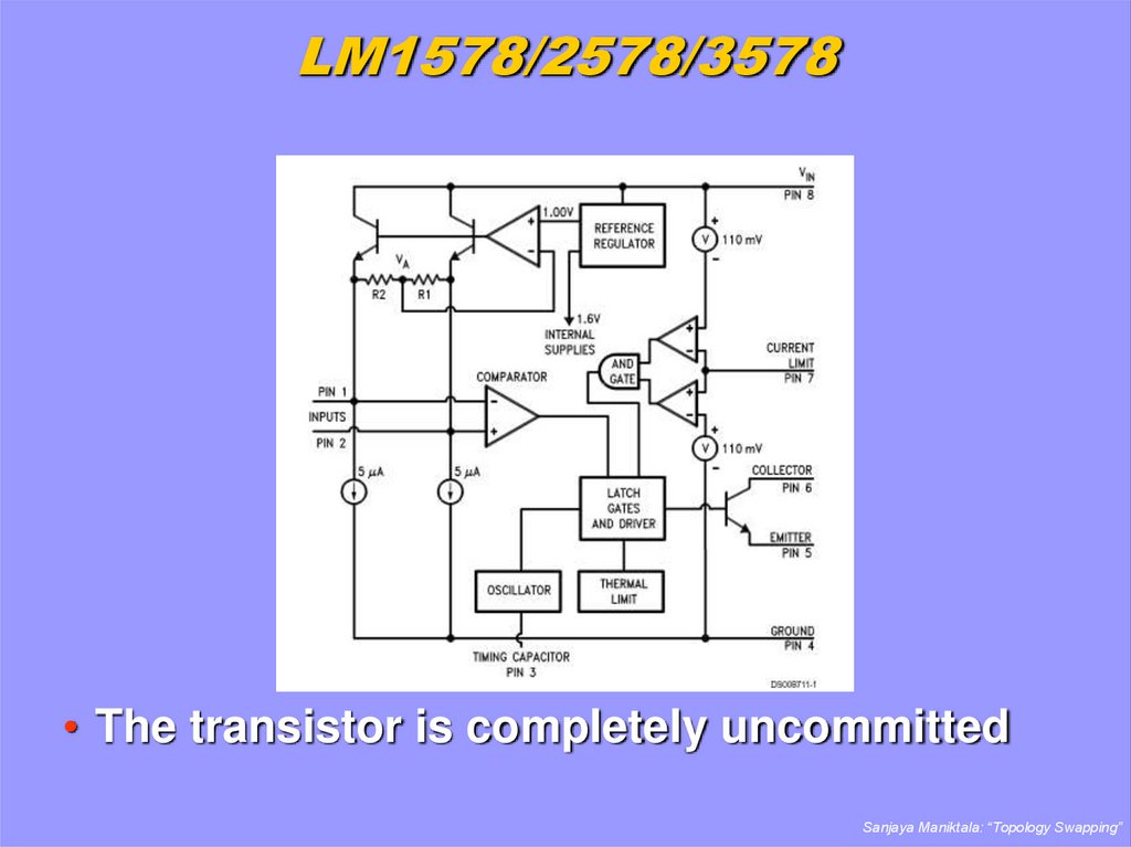
• Not very obvious, but this is a Type 1 IC!Sanjaya Maniktala: “Topology Swapping”
36. LM1578/2578/3578
• The transistor is completely uncommittedSanjaya Maniktala: “Topology Swapping”
37. LM1578 Applications
• From L to R: Pinout, +ve to +ve Boost, +ve to+ve Buck
Sanjaya Maniktala: “Topology Swapping”
38. Labeling of Pins
• Don’t be confused by the pin labels. There isunfortunately no uniformity. Different engineers have
used different labels. For example….
• In a Buck (Type 1), the switching node has been
called “Switch” , or “Output”.
• Therefore Identify the switching node: by definition
it is the node where the switch, diode and inductor
are connected
• But look at the Block Diagram first!!
Sanjaya Maniktala: “Topology Swapping”
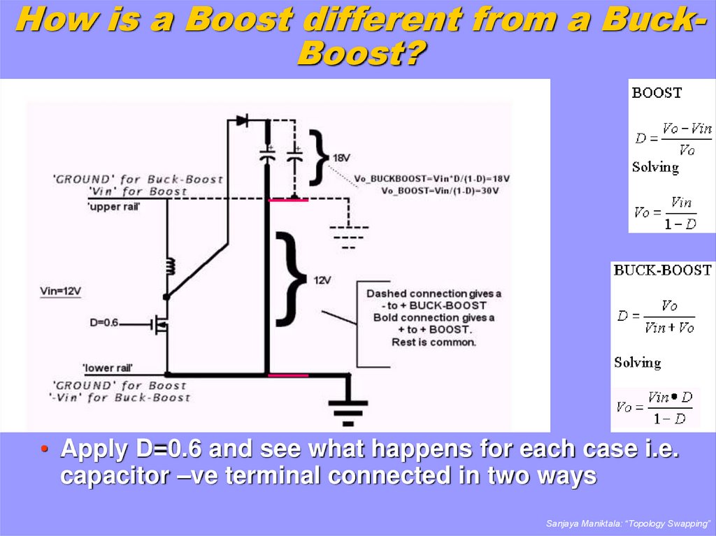
39. How is a Boost different from a Buck-Boost?
How is a Boost different from a BuckBoost?• Apply D=0.6 and see what happens for each case i.e.
capacitor –ve terminal connected in two ways
Sanjaya Maniktala: “Topology Swapping”
40. Boost and Buck-Boost compared
• The main difference is in the feedback. Since for aBoost, the IC control is typically always connected
to the ‘lower rail’, a simple resistive divider across
the output capacitor can be used to connect directly
to the feedback pin of the IC control. But for the
Buck-Boost, the output voltage is with respect to the
system ground (the ‘upper rail’), whereas the IC
control is still referenced to the ‘lower rail’.
Therefore a more elaborate solution is required. This
usually takes the form of a differential amplifier
stage to sense the output voltage of the Buck-Boost
and then to ‘translate’ it to the lower rail.
Sanjaya Maniktala: “Topology Swapping”
41. Nomenclature used
• In this article we will use the word ‘Flyback’to refer exclusively to a Buck-Boost stage
with inherent primary to secondary isolation.
Obviously this requires a transformer. But
we could also have a transformer-based
Buck-Boost with no isolation present,
because the primary and secondary
windings are connected together for easier
implementation of feedback.
Sanjaya Maniktala: “Topology Swapping”
42. Boost/Buck-Boost/what else??
Sanjaya Maniktala: “Topology Swapping”43.
• Now the crucial chain of logic behind hiddenapplications: the primary intended
application for the Type 1 is IC is the
positive to positive Boost. We know that this
involves a ‘N-’ cell (Type B). Therefore we
conclude that this IC is most ‘comfortable’
with any topology/configuration, provided it
involves a (similar) Type B cell. This Type B
cell is a ‘natural choice’ for a Type 1 IC.
Sanjaya Maniktala: “Topology Swapping”
44. Natural Choices of a Type 1 IC
• a)Positive to Positive Boost: Uses a Type
B cell. The primary intended Application for
a Type 1 IC.
• b)
Negative to Positive Buck-Boost: Uses
a Type B cell. Another intended Application
for a Type 1 IC.
• c)
Negative to Negative Buck: Uses a
Type B cell. A ‘hidden application’.
Sanjaya Maniktala: “Topology Swapping”
45. (Type B LSD Cell, Type 1 IC) +ve to +ve Boost
Sanjaya Maniktala: “Topology Swapping”46. (Type B LSD Cell, Type 1 IC) -ve to +ve Buck-Boost
Sanjaya Maniktala: “Topology Swapping”47. (Type B LSD Cell, Type 1 IC) -ve to -ve Buck
Sanjaya Maniktala: “Topology Swapping”48. (Type A LSD Cell, Type 1 IC) -ve to -ve Boost
Sanjaya Maniktala: “Topology Swapping”49. (Type A LSD Cell, Type 1 IC) +ve to -ve Buck-Boost
Sanjaya Maniktala: “Topology Swapping”50. (Type A LSD Cell, Type 1 IC) +ve to +ve Buck
Sanjaya Maniktala: “Topology Swapping”51. Summary of Type 1 IC Applications
Sanjaya Maniktala: “Topology Swapping”52. Natural Choices of a Type 2 IC
• a) Positive to Positive Buck: Uses a Type Acell. The primary intended Application for a
Type 2 IC.
• b) Positive to Negative Buck-Boost: Uses a
Type A cell. Additional IC bypass capacitor
required.
• c) Negative to Negative Boost: Uses a Type
A cell. Additional IC bypass capacitor
required.
Sanjaya Maniktala: “Topology Swapping”
53. (Type A LSD Cell, Type 2 IC) +ve to +ve Buck
Sanjaya Maniktala: “Topology Swapping”54. (Type A LSD Cell, Type 2 IC) +ve to -ve Buck-Boost
Sanjaya Maniktala: “Topology Swapping”55. (Type A LSD Cell, Type 2 IC) -ve to -ve Boost
Sanjaya Maniktala: “Topology Swapping”56. ‘Forced’ Choices for Type 2 IC?
• Because the Drain/Collector is NOTuncommitted, it is not possible to have a
Type 1 IC to perform in any application
involving a cell that was not its intended
cell. Therefore ‘forced’ choices are not
possible.
Sanjaya Maniktala: “Topology Swapping”
57. Summary of Type 2 IC Applications
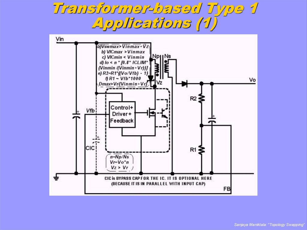
Sanjaya Maniktala: “Topology Swapping”58. Transformer-based Type 1 Applications (1)
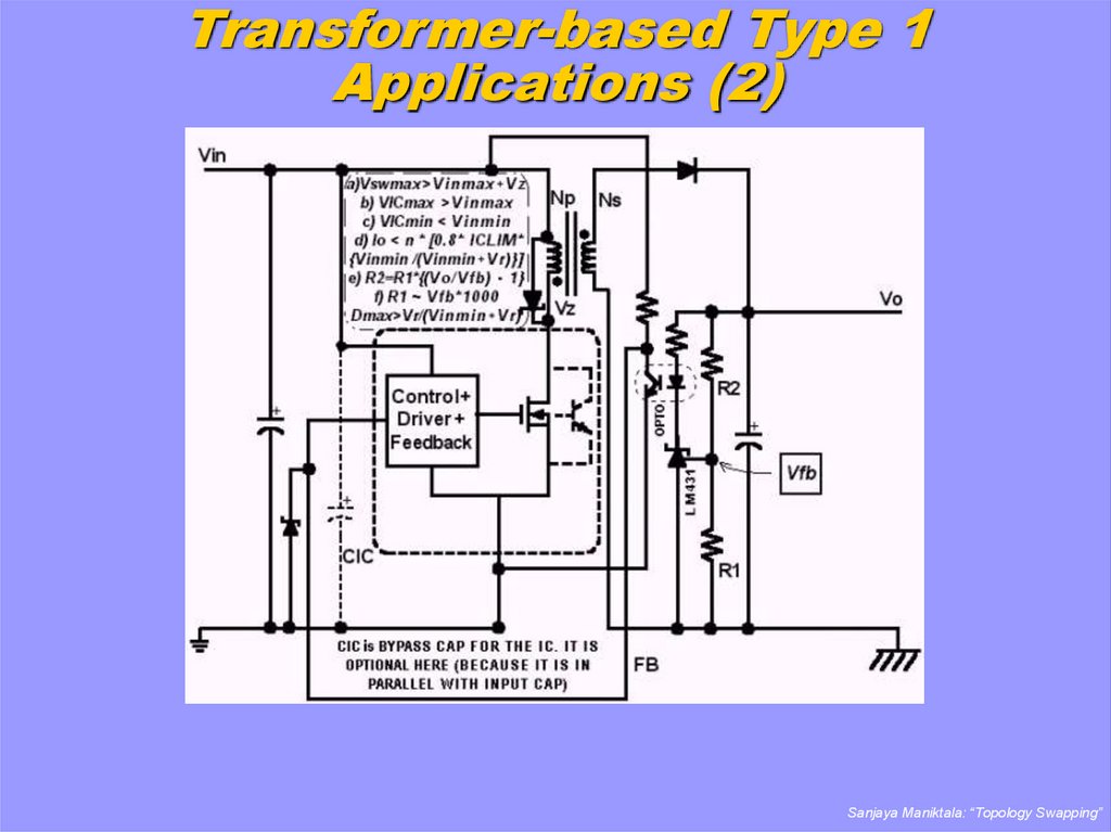
Sanjaya Maniktala: “Topology Swapping”59. Transformer-based Type 1 Applications (2)
Sanjaya Maniktala: “Topology Swapping”60. Differential Sensing Techniques (1)
Sanjaya Maniktala: “Topology Swapping”61. Differential Sensing Techniques (2)
Sanjaya Maniktala: “Topology Swapping”62. Equations for Differential Sense
Sanjaya Maniktala: “Topology Swapping”63. Summary of Applications
Sanjaya Maniktala: “Topology Swapping”64. Example 1
• The LM2585 is a ‘3A Flyback regulator’. Canit be used in a Boost topology? And for what
range?
The MIN value of its internal current limit is
3A. Its input operating voltage range is 4V to
40V. Its switch can withstand 65V.
Sanjaya Maniktala: “Topology Swapping”
65. Example 1 (contd)
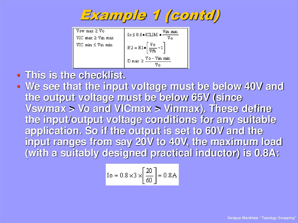
• This is the checklist.• We see that the input voltage must be below 40V and
the output voltage must be below 65V (since
Vswmax > Vo and VICmax > Vinmax). These define
the input/output voltage conditions for any suitable
application. So if the output is set to 60V and the
input ranges from say 20V to 40V, the maximum load
(with a suitably designed practical inductor) is 0.8A:
Sanjaya Maniktala: “Topology Swapping”
66. Example 2
• The required application conditions are Vinranging from 4.5V to 5.5V. The output
requirement is –5V at 0.5A. Can the LM2651
be used?
LM2651 is a ‘1.5A Buck Regulator’. Note
firstly that this IC can deliver 1.5A in a Buck
configuration, but not so in any other
configuration/topology. The load rating must
then be re-calculated
Sanjaya Maniktala: “Topology Swapping”
67. Example 2 (contd)
1.2.
Referring to the datasheet of this device we get :
VICmin=4V,VICmax=14V
ICLIM=1.55A. Dmax (MIN)=92%
Therefore we now check sequentially for these conditions:
a) VICmax>Vinmax+Vo
14V>5.5V+5V=10.5V
OK
b) VICmin<Vinmin 4V < 4.5V OK
c) Io< 0.8*ICLIM* (Vinmin/(Vinmin+Vo):
0.5< 0.8*1.55*{4.5/(4.5+5)}=0.587 OK
d) Dmax>Vo/(Vo+Vinmin)
0.92>5/(5+4.5)=0.53
OK
Therefore the LM2651 is acceptable for the intended application.
Sanjaya Maniktala: “Topology Swapping”
68. Nuances of Topology Swapping
• One of the main concerns when we jump topologieshas to do with a nuance of the topologies
themselves. In particular, we must remember that a
Buck topology has no Right Half Plane (‘RHP’) zero,
but the Boost and the Flyback/Buck-Boost do.
Therefore when we try to take a Buck IC (with
internal fixed compensation), we may not have the
ability to tailor the crossover frequency to less than
1/4th of the RHP zero frequency as is generally
recommended for avoiding this particular mode of
instability. So how do we successfully take a Type 2
IC and apply it to other topologies?
Sanjaya Maniktala: “Topology Swapping”
69. Conquering the RHP Zero (1)
Sanjaya Maniktala: “Topology Swapping”70. Conquering the RHP Zero (2)
Sanjaya Maniktala: “Topology Swapping”71. Conclusion
• This sums up a walk through those mysterious ‘hidden’applications of switchers. The average designer should
have no trouble extending these principles to
controllers and other types of switchers, not discussed
herein. For detailed information about how to actually
design switchers, please see:
References
• a)
Application Note AN-1197 at
http://power.national.com
• b)
Application Note AN-1246 at
http://power.national.com
Sanjaya Maniktala: “Topology Swapping”
























 electronics


