


 electronics
Similar presentations:
")


![PBA Repair Guide [GT-S8000]](https://cf.ppt-online.org/files/thumb/t/tIHBnfpml5G6E47aLocdVU0kDZQNvuejRhAMC8.jpg "PBA Repair Guide [GT-S8000]")
")


HW Repair Guide GT-N5100 (Galaxy Note 8.0)
1.
HW Repair GuideGT-N5100 (Galaxy Note 8.0)
March, 2013
© Samsung Electronics Co., LTD |
Confidential
2.
NOTICE1. All functionality, features, specifications and other product
information provided in this document including, but not limited
to, the benefits, design, pricing, components, performance,
availability, and capabilities of the product are subject to change
without notice or obligation. Samsung reserves the right to make changes to this docume
nt and the product described herein, at anytime, without obligation on Samsung to provid
e notification of such change.
2. In data of our company, important management / technical information is included,
and if it is leaked, loss can happen in various aspect such as closing a technology gap,
increasing ability to respond.
Therefore, it is strictly prohibited from information leak or forwarding this material, and if
leak of management / technical information due to disobeying the law happens, it can be
severely punished in accordance with information protection rule of our company.
© Samsung Electronics Co., LTD |
Confidential
2
3.
Contents1.
Introduction of GALAXY Note 8
2.
Service Guide
RF calibration
IMEI writing
Block Diagram
3.
Repair Guide
Assembly & Disassembly
Electronic Components
4.
SMD parts
Trouble Shooting
Q&A
© Samsung Electronics Co., LTD |
Confidential
3
4.
Introduction of GALAXY Note 8.0Specification
This model is the portable media Tablet device and it has 8 inches size.
So, it expected to replace the diary and it has S-pen, S-planner, S-Note, etc.
Item
spec.
AP
1.6GHz Quad Core(Exynos 4412)
OS
Android JB
CP
XMM6262(IMC), HSPA+ 21.1Mbps, HSUPA 5.76Mbps
Supported RF Bands
GSM Quad(850, 900, 1800, 1900), UMTS Quad(850, 900, 1800, 1900)
Internal Memory
16GB NAND + 2GB RAM
External Memory
MicroSD (up to 64GB)
Display
8” TFT (1280 x 800)
Camera
5MP CMOS + 1.3MP CMOS
Sensor
Accelerometer, Magnetic, Proximity, Light, Grip
Connectivity
BT 4.0, Wi-Fi a/b/g/n
GPS
A-GPS + GLONASS
Battery
4600mA
© Samsung Electronics Co., LTD |
Confidential
4
5.
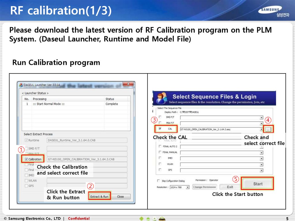
RF calibration(1/3)Please download the latest version of RF Calibration program on the PLM
System. (Daseul Launcher, Runtime and Model File)
Run Calibration program
Check the CAL
Check and
select correct file
Check the Calibration
and select correct file
Click the Extract
& Run button
© Samsung Electronics Co., LTD |
Confidential
Click the Start button
5
6.
RF calibration(2/3)Type the correct
H/W version
Click the
Model Information
Check the Calibration
Click the
Hardware Config
Check the
System Config items
Click the
OK button
Check the connection port of
Phone, MSTS and Power Supply
© Samsung Electronics Co., LTD |
Confidential
6
7.
RF calibration(3/3)The Result bar is changed to the GREEN
color if the calibration is Passed.
Click the Start button and
connect the phone to Anyway Jig.
© Samsung Electronics Co., LTD |
Confidential
7
8.
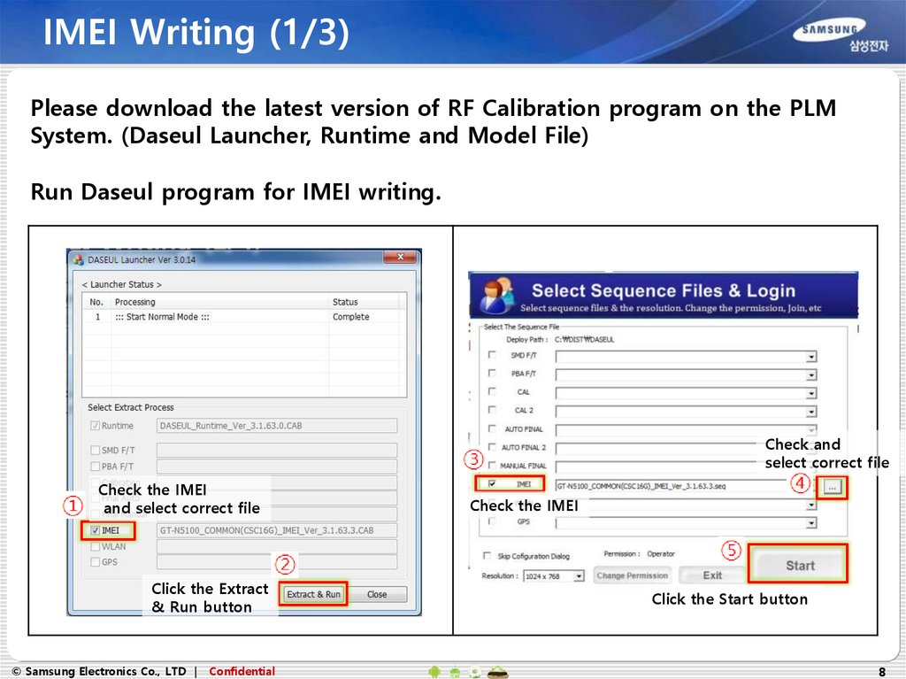
IMEI Writing (1/3)Please download the latest version of RF Calibration program on the PLM
System. (Daseul Launcher, Runtime and Model File)
Run Daseul program for IMEI writing.
Check and
select correct file
Check the IMEI
and select correct file
Click the Extract
& Run button
© Samsung Electronics Co., LTD |
Confidential
Check the IMEI
Click the Start button
8
9.
IMEI Writing (2/3)Check the IMEI Write
and IMEI Check
Click the
Hardware
Config
Check the
System Config items
Check the
OK button
© Samsung Electronics Co., LTD |
Confidential
Check the connection port of
Phone and Power Supply
9
10.
IMEI Writing (3/3)Type the correct
Software, Hardware,
CSC, PDA and
SKU_CODE etc.
Click the Start button and
connect the phone to Anyway Jig.
Type the correct
IMEI number
The Status bar is changed to
GREEN color if IMEI writing is Passed
Click the Model Info
© Samsung Electronics Co., LTD |
Confidential
10
11.
Block Diagram© Samsung Electronics Co., LTD |
Confidential
11
12.
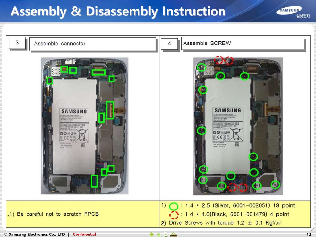
Assembly & Disassembly Instruction<Assembly>
© Samsung Electronics Co., LTD |
Confidential
12
13.
Assembly & Disassembly Instruction© Samsung Electronics Co., LTD |
Confidential
13
14.
Assembly & Disassembly Instruction© Samsung Electronics Co., LTD |
Confidential
14
15.
Assembly & Disassembly Instruction<Disassembly>
© Samsung Electronics Co., LTD |
Confidential
15
16.
Assembly & Disassembly Instruction© Samsung Electronics Co., LTD |
Confidential
16
17.
Assembly & Disassembly Instruction© Samsung Electronics Co., LTD |
Confidential
17
18.
Electronic ComponentsMain Antenna
GH42-03975A
1.3M
CAM
GH96-06106A
BT/WIFI/GPS
Antenna
(on the rear cover)
SD card socket/
Motor module
GH59-13124A
WACOM
connector
5M
CAM
GH96-05974A
GH42-03977A
Sub MIC/
Power-volume key/
IrDA Module
GH59-12911A
GH59-12908A
SPK(R)/
Main MIC
Module
S-Pen
GH98-25480A
TSP connector
Receiver/
3.5pi Ear Jack/
Light-Proximity
sensor Module
GH59-12906A
LCD connector
GH59-12919A
11pin sub PCB
(including SPK(R) connector
and Home key FPCB connector
GH59-13128A
Home
key FPCB
GH59-12910A
SIM card
socket
GH59-13117A
SPK(L)
Module
© Samsung Electronics Co., LTD |
Confidential
GH59-12907A
18
19.
SMD parts (TOP side)Ant100, Ant101 3712-001375
Ant. Contact (for GSM, WCDMA)
U1001
1204-003387
IrDA IC
U900
1209-002142
Magnetic Sensor
OSC200
2805-001098
Oscillator – 26MHz
UME600
1107-002190
MoviNAND
U201 1205-004649
GPS IC (inside of shield-can)
UCD400
1205-004510
Audio CODEC
HDC900 3708-002222
Connector (5M Camera)
U702
1203-006346
Reset IC
U701
1203-007657
PMIC
© Samsung Electronics Co., LTD |
Confidential
19
20.
SMD parts (Bottom side)U106 1209-002006
Grip Sensor IC
Ant202, Ant203 3712-001375
Ant. Contact (for BT, WIFI, GPS)
U203 1205-004598
Bluetooth & WIFI IC
(inside of shield-can)
U105 1203-006801
Transceiver DCDC
OSC100 2801-005166
DCXO – 26MHz
HDC1000 3711-006923
Connector(Power & Vol & IrDA)
U100 1205-004515
Transceiver
HDC901 3711-006925
Connector (1.3M Camera)
U904 1205-004521
TSP IC
HDC402 3711-007188
Connector (Receiver & Ear Jack
& Light-Proximity sensor)
C1013
U901 1209-002153
Acc. Sensor
HDC800 3711-007295
Connector (LCD)
HDC500 3711-007173
Connector (SD card & Motor)
SLC1000 3708-003131
Connector (WACOM)
F100 2911-000236
Antenna Switch Module
U104 1203-007333
PAM DCDC
PAM100 1201-003400
Power Amplifier Module
1205-004233
MHL IC
UCP600 0902-002996
Application Processor
BTC700 3711-008421
Connector (Battery)
HDC300 3711-008347
Connector (SIM)
IFC500 3711-006843
Connector (11pin sub PCB)
© Samsung Electronics Co., LTD |
F101 2910-000190
SAW Duplexer
U1008 1205-004674
WACOM IC
Confidential
SLC900 3708-002781
Connector (TSP)
UME300 1105-002212
Mobile DDR SDRAM
UCP300 1205-004511
Call Processor
U705
1203-007321
IF PMIC
HDC400 3711-008347
Connector (SPK-L)
20
21.
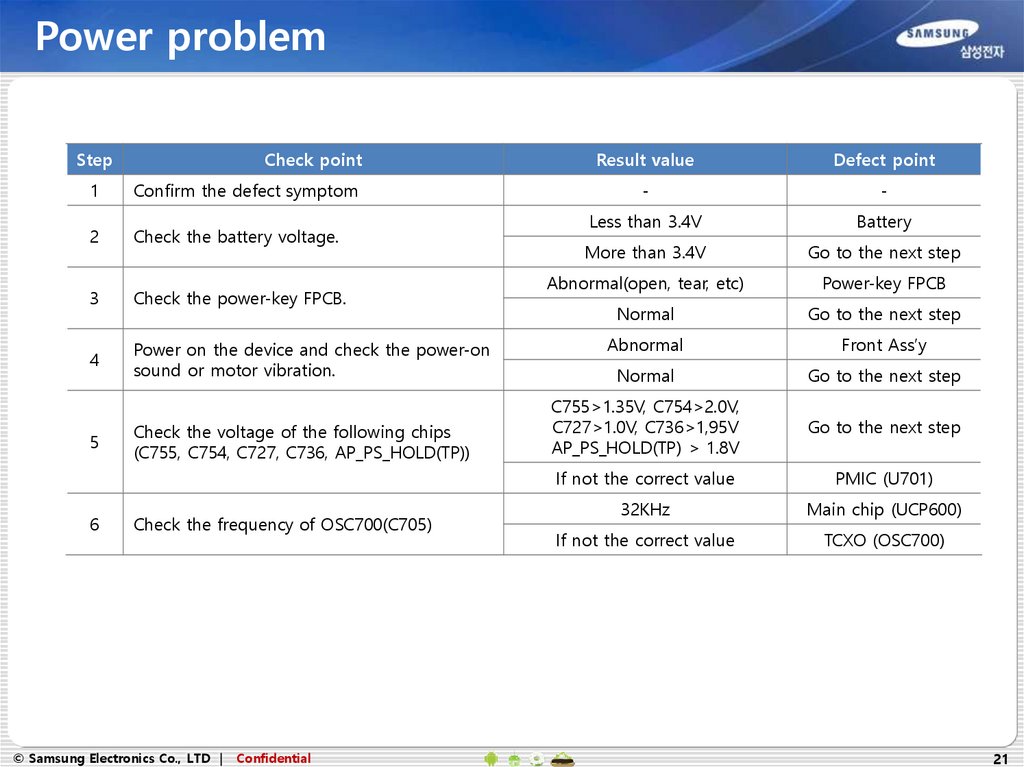
Power problemStep
Check point
1
Confirm the defect symptom
2
Check the battery voltage.
3
Check the power-key FPCB.
4
Power on the device and check the power-on
sound or motor vibration.
5
6
Check the voltage of the following chips
(C755, C754, C727, C736, AP_PS_HOLD(TP))
Check the frequency of OSC700(C705)
© Samsung Electronics Co., LTD |
Confidential
Result value
Defect point
-
-
Less than 3.4V
Battery
More than 3.4V
Go to the next step
Abnormal(open, tear, etc)
Power-key FPCB
Normal
Go to the next step
Abnormal
Front Ass’y
Normal
Go to the next step
C755>1.35V, C754>2.0V,
C727>1.0V, C736>1,95V
AP_PS_HOLD(TP) > 1.8V
Go to the next step
If not the correct value
PMIC (U701)
32KHz
Main chip (UCP600)
If not the correct value
TCXO (OSC700)
21
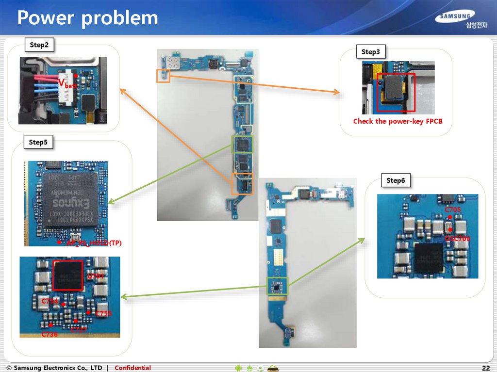
22.
Power problemStep2
Step3
Vbatt
Check the power-key FPCB
Step5
Step6
C705
AP_PS_HOLD(TP)
OSC700
U701
C754
C755
C736
C727
© Samsung Electronics Co., LTD |
Confidential
22
23.
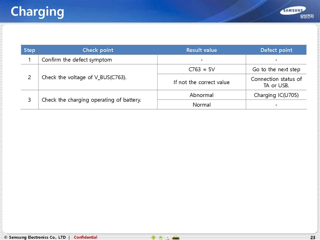
ChargingStep
1
Check point
Confirm the defect symptom
2
Check the voltage of V_BUS(C763).
3
Check the charging operating of battery.
© Samsung Electronics Co., LTD |
Confidential
Result value
Defect point
-
-
C763 = 5V
Go to the next step
If not the correct value
Connection status of
TA or USB.
Abnormal
Charging IC(U705)
Normal
-
23
24.
ChargingStep2, 3
U705
Charging IC
C763
© Samsung Electronics Co., LTD |
Confidential
24
25.
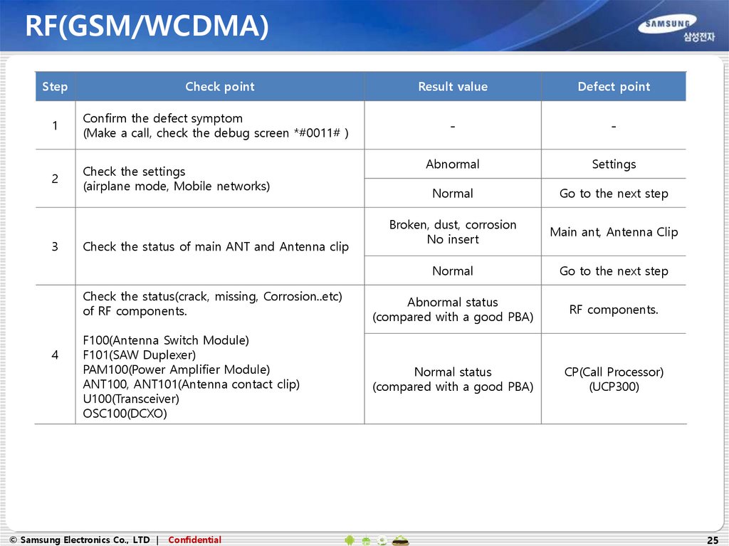
RF(GSM/WCDMA)Step
Check point
Result value
Defect point
-
-
Abnormal
Settings
Normal
Go to the next step
Broken, dust, corrosion
No insert
Main ant, Antenna Clip
Normal
Go to the next step
Check the status(crack, missing, Corrosion..etc)
of RF components.
Abnormal status
(compared with a good PBA)
RF components.
F100(Antenna Switch Module)
F101(SAW Duplexer)
PAM100(Power Amplifier Module)
ANT100, ANT101(Antenna contact clip)
U100(Transceiver)
OSC100(DCXO)
Normal status
(compared with a good PBA)
CP(Call Processor)
(UCP300)
1
Confirm the defect symptom
(Make a call, check the debug screen *#0011# )
2
Check the settings
(airplane mode, Mobile networks)
3
4
Check the status of main ANT and Antenna clip
© Samsung Electronics Co., LTD |
Confidential
25
26.
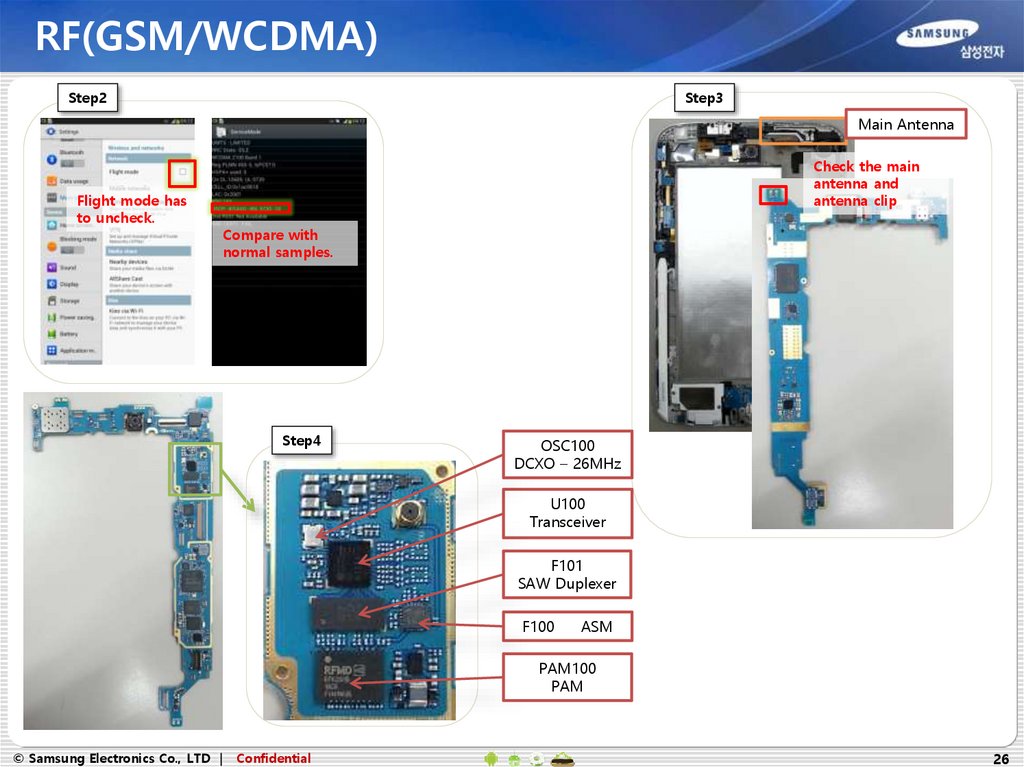
RF(GSM/WCDMA)Step2
Step3
Main Antenna
Flight mode has
to uncheck.
Check the main
antenna and
antenna clip
Compare with
normal samples.
Step4
OSC100
DCXO – 26MHz
U100
Transceiver
F101
SAW Duplexer
F100
ASM
PAM100
PAM
© Samsung Electronics Co., LTD |
Confidential
26
27.
SIM card detection problemStep
1
2
3
4
Check point
Confirm the defect symptom
Check the SIM socket & Connector(HDC300)
Check the voltage of detection pin
(R330)
Notice. It should be measured when the
phone is started
Check the voltage of SIM
(R331)
Notice. It should be measured when the
phone started
© Samsung Electronics Co., LTD |
Confidential
Result value
Defect point
-
-
Broken, dust, corrosion
SIM socket or
Connector
Normal
Go to the next step
R330 = 1.8V
Go to the next step
If not the correct value
SIM Card
R331 = 3V
PBA
If not the correct value
CP(UCP300)
27
28.
SIM card detection problemStep2, 3, 4
R330
R331
HDC300
SIM socket connector
SIM socket
© Samsung Electronics Co., LTD |
Confidential
28
29.
Microphone ProblemStep
Check point
1
Confirm the defect symptom
2
Check the microphone hole
3
Check the microphone rubber
4
Check the MIC FPCB status
Check the voltage of C413
5
Notice. It should be measured when the
microphone path is activated on
Check the signal of C418, C419
6
Notice. It should be measured when the
microphone path is activated on
© Samsung Electronics Co., LTD |
Confidential
Result value
Defect point
-
-
Dust
Clean the hole
Normal
Go to the next step
Wrong insert
Re-insert
Normal
Go to the next step
Abnormal
Speaker(R)-MIC module
Normal
Go to the next step
2.8V
Go to the next step
If not the correct value
MIC LDO(U401)
Same signal compared with a
good PBA
Microphone
If not the correct value
AUDIO CODEC(UCD400)
29
30.
Microphone ProblemStep2, 3
Step4
Check the MIC
hole and rubber
Check the MIC
FPCB status
Step6
C418
C419
Step5
UCD400
Audio CODEC
U401
C413
© Samsung Electronics Co., LTD |
Confidential
30
31.
Speaker ProblemStep
Check point
Result value
Defect point
-
-
Solved
Setting error
Not solved
Go to the next step
Broken, dust, corrosion
Speaker connector
Normal
Go to the next step
Solved
speaker
Not solved
Go to the next step
Check the signals on
L406, L407 of Left Speaker in main PCB,
C105, C106 of Right Speaker in Sub PCB.
Same signal compared with a
good PBA
Speaker
Notice. It should be measured when the
speaker path is activated on
If not the correct value
Audio Codec (UCD400)
1
Confirm the defect symptom
2
Make a factory reset (*2767*3855#)
3
Check the speaker connector (HDC400(L) in
Main PCB, HDC101(R) in Sub PCB)
4
Replace the speaker module
5
© Samsung Electronics Co., LTD |
Confidential
31
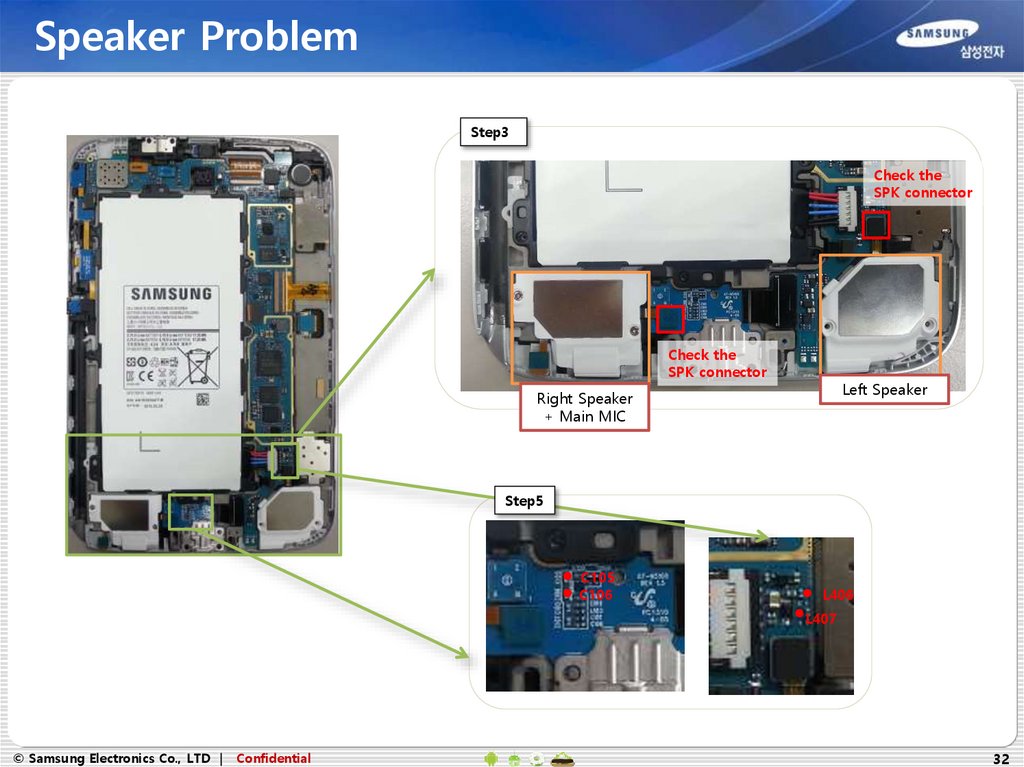
32.
Speaker ProblemStep3
Check the
SPK connector
Check the
SPK connector
Left Speaker
Right Speaker
+ Main MIC
Step5
C105
C106
L406
L407
© Samsung Electronics Co., LTD |
Confidential
32
33.
BT/WIFI ProblemStep
Check point
Result value
Defect point
1
Confirm the defect symptom
(Check the turned on BT/WIFI & connected device)
Turned on
Go to the next step
Turned off
Turn on
2
Check the BT/WIFI Ant. & Ant contact.
(Rear cover Ant. & ANT202, ANT203)
Broken, dust, corrosion
BT/WIFI Ant &
ANT202, ANT203
Normal
Go to the next step
C233 = 1.8V
Go to the next step
Notice. It should be measured when the BT/WIFI
path is activated on
If not the correct value
PMIC (U701)
Check the clock of C250, C251
C250, C251 = 37Mhz
(Same signal compared
with a good PBA)
BT/WIFI IC (U203)
If not the correct value
OSC201
Check the voltage of C233
3
4
Notice. It should be measured when the BT/WIFI
path is activated on
© Samsung Electronics Co., LTD |
Confidential
33
34.
BT/WIFI ProblemStep1
You can check the this layout
if open the shied cover
Check the turn on
Step2, 3, 4
ANT202, ANT203
Step2
BT/WIFI Antenna
U203
BT/WIFI IC
C251
OSC201
C250
© Samsung Electronics Co., LTD |
Confidential
C233
34
35.
GPS/GLONASS ProblemStep
Check point
Result value
Defect point
Turned on
Go to the next step
Turned off
Turn on
1
Confirm the defect symptom
(Check the turned on GPS function)
2
Check the BT/WIFI Ant. & Ant contact.
(Rear cover Ant. & ANT202, ANT203)
Broken, dust, corrosion
BT/WIFI Ant &
ANT202, ANT203
Normal
Go to the next step
Check the voltage of C209, C211, L200
C209 = 1.8V
C211, L200 = 2.8V
Go to the next step
Notice. It should be measured when the GPS path
is activated on
If not the correct value
PMIC(U701)
Check the clock of C200,C201(OSC200)
C200,C201 = 26Mhz
(Same signal compared
with a good PBA)
GPS IC(U201)
GPS LNA(U200)
If not the correct value
OSC200
3
4
Notice. It should be measured when the GPS path
is activated on
© Samsung Electronics Co., LTD |
Confidential
35
36.
GPS/GLONASS ProblemStep1
Check the turn on
Step3, 4
Step2
C209
ANT202, ANT203
BT/WIFI Antenna
© Samsung Electronics Co., LTD |
U201
GPS IC
L200
C211
U200
OSC200
C200 C201
Confidential
36
37.
Display ProblemStep
1
2
3
4
5
Check point
Confirm the defect symptom
Check the LCD connector (HDC800)
Check the signal or voltage of C804 and C806
Notice. It should be measured when the display is
activated on
Check the voltage of C800 and C801
Notice. It should be measured when the display is
activated on
Replace the LCD
© Samsung Electronics Co., LTD |
Confidential
Result value
Defect point
-
-
Broken, dust, corrosion
Insert status
LCD connector
(HDC800)
Normal
Go to the next step
If not the correct value
LED Backlight IC(U802)
Normal(C804 = high(18V),
C806 = V_BATT)
Go to the next step
If not the correct value
Buck boost Reg.(U800)
Normal(C800 = V_BATT,
C801 = 3.3V)
Go to the next step
Solved
LCD
Not solved
Main Chip or PBA
37
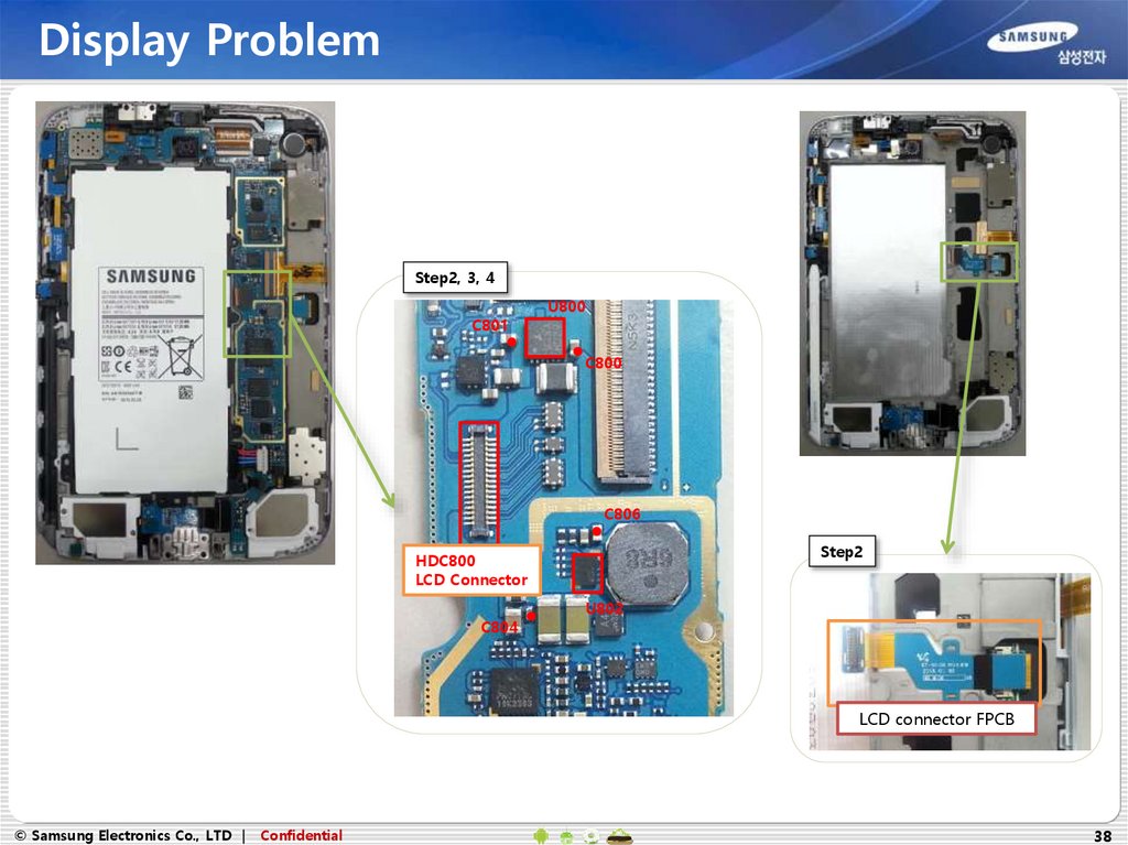
38.
Display ProblemStep2, 3, 4
C801
U800
C800
C806
Step2
HDC800
LCD Connector
C804
U802
LCD connector FPCB
© Samsung Electronics Co., LTD |
Confidential
38
39.
Touch ProblemStep
Result value
Defect point
-
-
Broken, dust, corrosion
TSP connector
(SLC900)
Normal
Go to the next step
If not the correct value
TSP LDO(U902)
3
Check the voltage of C913
Notice. It should be measured when the
display is activated on
C913 = 1.8V
Go to the next step
If not the correct value
Touch Sensor IC(U904)
4
Check the voltage of C902, C903
Notice. It should be measured when the
display is activated on
C902 = 3.3V
C903 = 1.8V
Go to the next step
If not the correct value
5
Check the Signal of following chips
(ZD903, ZD904, ZD905, R908, R682, R683)
Notice. It should be measured when the
display is activated on
ZD903, ZD904, ZD905,
R908, R682, R683
Same signal compared with a
good PBA
Go to the next step
Solved
TSP
Not solved
Main chip or PBA
1
2
6
Check point
Confirm the defect symptom
Check the TSP connector (SLC900)
Replace the TSP
© Samsung Electronics Co., LTD |
Confidential
39
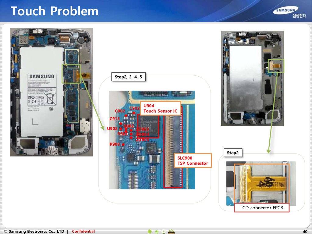
40.
Touch ProblemStep2, 3, 4, 5
C902
C903
U904
Touch Sensor IC
C913
R682
U902
ZD903
R683
ZD904
ZD905
R908
SLC900
TSP Connector
Step2
LCD connector FPCB
© Samsung Electronics Co., LTD |
Confidential
40
41.
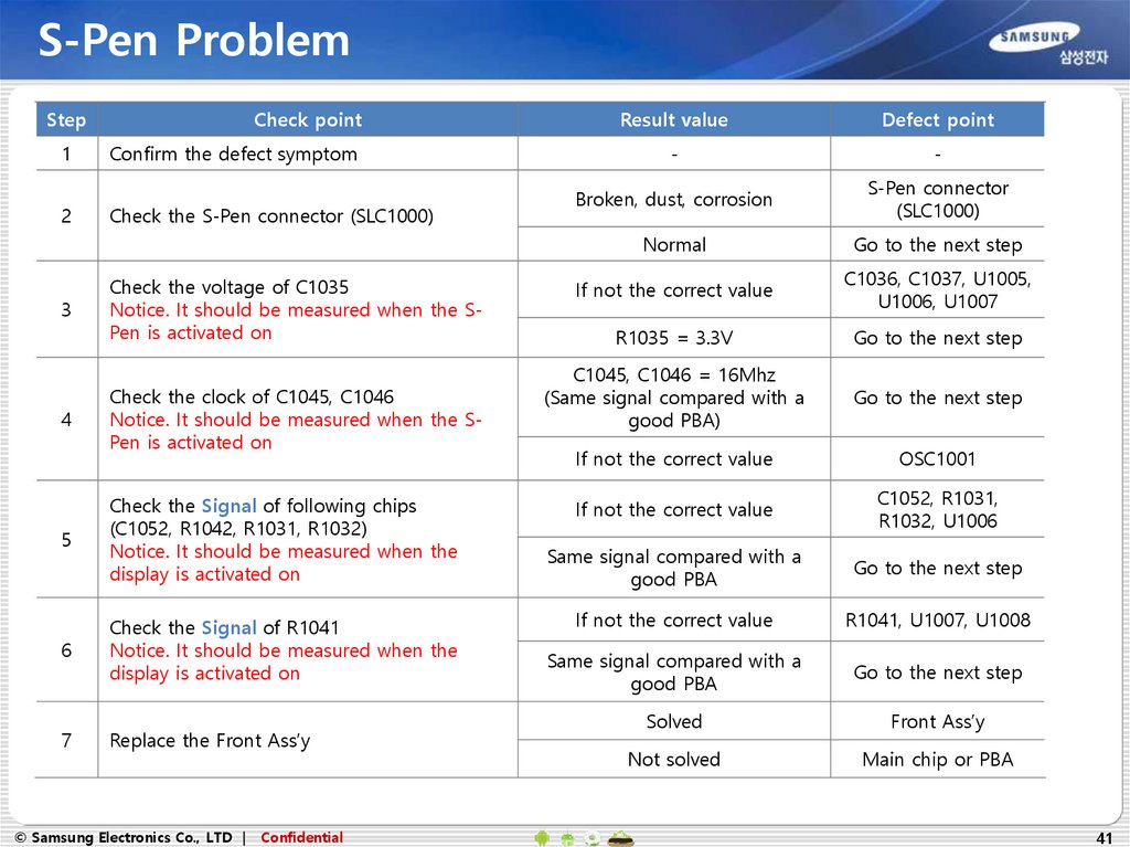
S-Pen ProblemStep
1
2
3
4
5
Check point
Confirm the defect symptom
Check the S-Pen connector (SLC1000)
Check the voltage of C1035
Notice. It should be measured when the SPen is activated on
Check the clock of C1045, C1046
Notice. It should be measured when the SPen is activated on
Check the Signal of following chips
(C1052, R1042, R1031, R1032)
Notice. It should be measured when the
display is activated on
6
Check the Signal of R1041
Notice. It should be measured when the
display is activated on
7
Replace the Front Ass’y
© Samsung Electronics Co., LTD |
Confidential
Result value
Defect point
-
-
Broken, dust, corrosion
S-Pen connector
(SLC1000)
Normal
Go to the next step
If not the correct value
C1036, C1037, U1005,
U1006, U1007
R1035 = 3.3V
Go to the next step
C1045, C1046 = 16Mhz
(Same signal compared with a
good PBA)
Go to the next step
If not the correct value
OSC1001
If not the correct value
C1052, R1031,
R1032, U1006
Same signal compared with a
good PBA
Go to the next step
If not the correct value
R1041, U1007, U1008
Same signal compared with a
good PBA
Go to the next step
Solved
Front Ass’y
Not solved
Main chip or PBA
41
42.
S-Pen ProblemStep2
S-Pen connector FPCB
Step2, 3, 4, 5, 6
SLC1000
S-Pen Connector
U1008
S-Pen IC
R1042
C1052
C1045
R1041
C1036
C1037
C1035
U1005
U1007
© Samsung Electronics Co., LTD |
Confidential
C1046
OSC1001
R1031
R1032
U1006
42
43.
5M CAM ProblemStep
Result value
Defect point
-
-
Broken, dust, corrosion
5M CAM connector
(HDC900)
Normal
Go to the next step
If not the correct value
C917, C920,
C921, C922
C917 = 1.2V, C920 = 1.8V,
C921 = 2.8V, C922 = 2.8V
Go to the next step
R906 = 24Mhz
(Same signal compared with a
good PBA)
Go to the next step
If not the correct value
Main chip
Check the Signal of following Test Point
(TP CAM I900, TP CAM I901)
Notice. It should be measured when the 5M
CAM is activated on
Same signal compared with a
good PBA
Go to the next step
If not the correct value
R678, R679
6
Check the F900, F901
Notice. It should be measured when the 5M
CAM is activated on
Abnormal
F900, F901
Normal
Go to the next step
7
Replace the 5M CAM
Solved
5M CAM
Not solved
Main chip or PBA
1
2
3
4
5
Check point
Confirm the defect symptom
Check the 5M CAM connector (HDC900)
Check the voltage of following chips
(C917, C920, C921, C922)
Notice. It should be measured when the 5M
CAM is activated on
Check the clock of R906
Notice. It should be measured when the 5M
CAM is activated on
© Samsung Electronics Co., LTD |
Confidential
43
44.
5M CAM ProblemStep5
Step2, 3, 4, 5, 6
R678
R679
C920
C917
R906
F901
F900
C921
Step7
5M CAM Module
C922
TP_CAM_I900
TP_CAM_I901
HDC900
5M CAM connector
© Samsung Electronics Co., LTD |
Confidential
44
45.
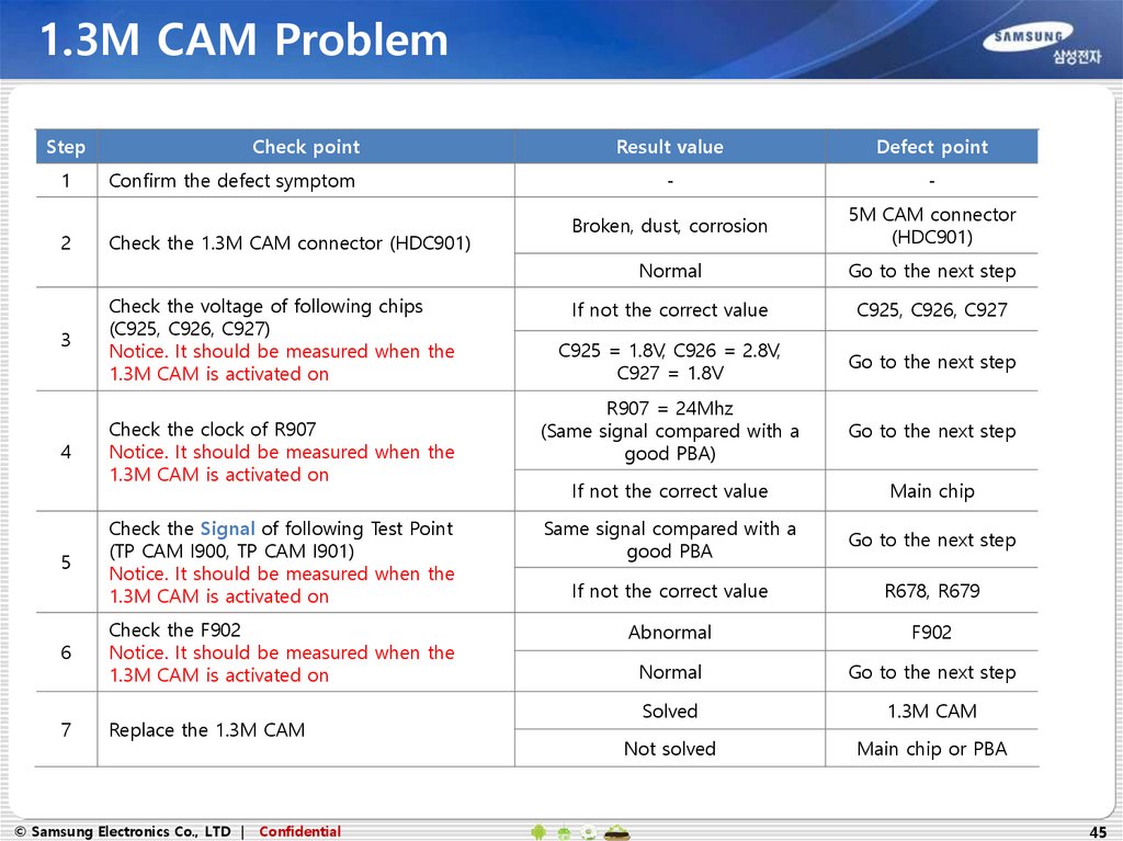
1.3M CAM ProblemStep
Result value
Defect point
-
-
Broken, dust, corrosion
5M CAM connector
(HDC901)
Normal
Go to the next step
If not the correct value
C925, C926, C927
C925 = 1.8V, C926 = 2.8V,
C927 = 1.8V
Go to the next step
R907 = 24Mhz
(Same signal compared with a
good PBA)
Go to the next step
If not the correct value
Main chip
Check the Signal of following Test Point
(TP CAM I900, TP CAM I901)
Notice. It should be measured when the
1.3M CAM is activated on
Same signal compared with a
good PBA
Go to the next step
If not the correct value
R678, R679
6
Check the F902
Notice. It should be measured when the
1.3M CAM is activated on
Abnormal
F902
Normal
Go to the next step
7
Replace the 1.3M CAM
Solved
1.3M CAM
Not solved
Main chip or PBA
1
2
Check point
Confirm the defect symptom
Check the 1.3M CAM connector (HDC901)
3
Check the voltage of following chips
(C925, C926, C927)
Notice. It should be measured when the
1.3M CAM is activated on
4
Check the clock of R907
Notice. It should be measured when the
1.3M CAM is activated on
5
© Samsung Electronics Co., LTD |
Confidential
45
46.
1.3M CAM ProblemStep4
R907
Step2, 3, 6
HDC901
1.3M CAM connector
Step5
F902
C925
C927 C926
TP_CAM_I900
TP_CAM_I901
Step5
Step7
1.3M CAM Module
R678
R679
© Samsung Electronics Co., LTD |
Confidential
46
47.
OTG ProblemStep
Check point
1
Confirm the defect symptom
2
Check the voltage of V_BUS(C763)
3
Check the voltage of V_BUS_IN(C506)
4
Replace the Sub PCB
© Samsung Electronics Co., LTD |
Confidential
Result value
Defect point
-
-
C763 = 5V
Go to the next step
If not the correct value
Charging IC(U705)
C506 = 5V
Go to the next step
If not the correct value
Charge protection
(U504)
Solved
Sub PCB
Not solved
Main chip or PBA
47
48.
OTG ProblemStep2
U705
C763
Step4
Step3
C506
Sub PCB
U504
© Samsung Electronics Co., LTD |
Confidential
48
49.
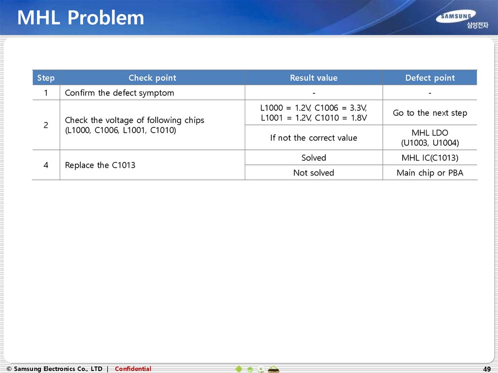
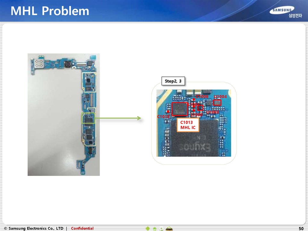
MHL ProblemStep
1
2
4
Check point
Confirm the defect symptom
Check the voltage of following chips
(L1000, C1006, L1001, C1010)
Replace the C1013
© Samsung Electronics Co., LTD |
Confidential
Result value
Defect point
-
-
L1000 = 1.2V, C1006 = 3.3V,
L1001 = 1.2V, C1010 = 1.8V
Go to the next step
If not the correct value
MHL LDO
(U1003, U1004)
Solved
MHL IC(C1013)
Not solved
Main chip or PBA
49
50.
MHL ProblemStep2, 3
C1006
U1004
L1001
C1010
L1000
U1003
C1013
MHL IC
© Samsung Electronics Co., LTD |
Confidential
50
51.
Q&AQuestion
© Samsung Electronics Co., LTD |
Confidential
51