Similar presentations:
Lenovo S660 Service Manual
1.
Company confidentialLenovo S660 Service Manual
Publisher NJD HW Team
Date 2014.02.28
2.
Function BlockCompany confidential
2
3.
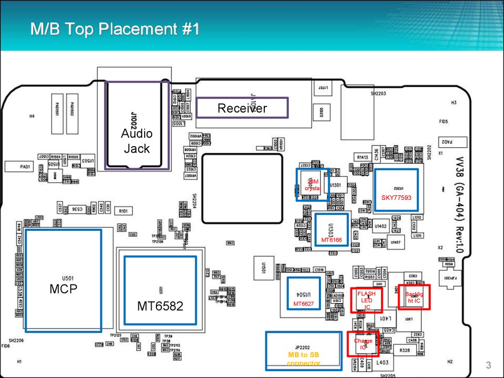
M/B Top Placement #1Receiver
Audio
Jack
26M
crystal
SKY77593
MT6166
MCP
MT6582
MT6627
FLASH
LED
IC
Backlig
ht IC
Charge
IC
Company confidential
MB to SB
connector
3
4.
M/B Bottom Placement #2TP
Connector
G-Sensor
Mic 2
P/L
Sensor
Connector
Audi
o PA
BACK UP
BATTERY
Camera
Connector
32K
crystal
DUAL SIM CONNECTOR
TF CARD CONNECTOR
LCM
connector
MT6323
Battery connector
Company confidential
4
5.
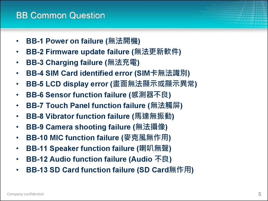
BB Common QuestionBB-1 Power on failure (無法開機)
BB-2 Firmware update failure (無法更新軟件)
BB-3 Charging failure (無法充電)
BB-4 SIM Card identified error (SIM卡無法識別)
BB-5 LCD display error (畫面無法顯示或顯示異常)
BB-6 Sensor function failure (感測器不良)
BB-7 Touch Panel function failure (無法觸屏)
BB-8 Vibrator function failure (馬達無振動)
BB-9 Camera shooting failure (無法攝像)
BB-10 MIC function failure (麥克風無作用)
BB-11 Speaker function failure (喇叭無聲)
BB-12 Audio function failure (Audio 不良)
BB-13 SD Card function failure (SD Card無作用)
Company confidential
5
6.
BB-1 Can not power on (無法開機) (1/3)1. Check if battery power level is low (確認電池是否有電?)
– VBATT (TP09 > 3.6V)
2. Check if J802 soldering condition is good (確認J802吃錫狀況是否正常?)
3. Check if power button is functional (確認開機鍵是否正常?)
– PWRKEY(TP11 > 2.8V)
– TP11 connect with ground wire to power on (跟地短路後可將系統開機)
TP11 > 2.8V
TP09 > 3.6V
Company confidential
6
7.
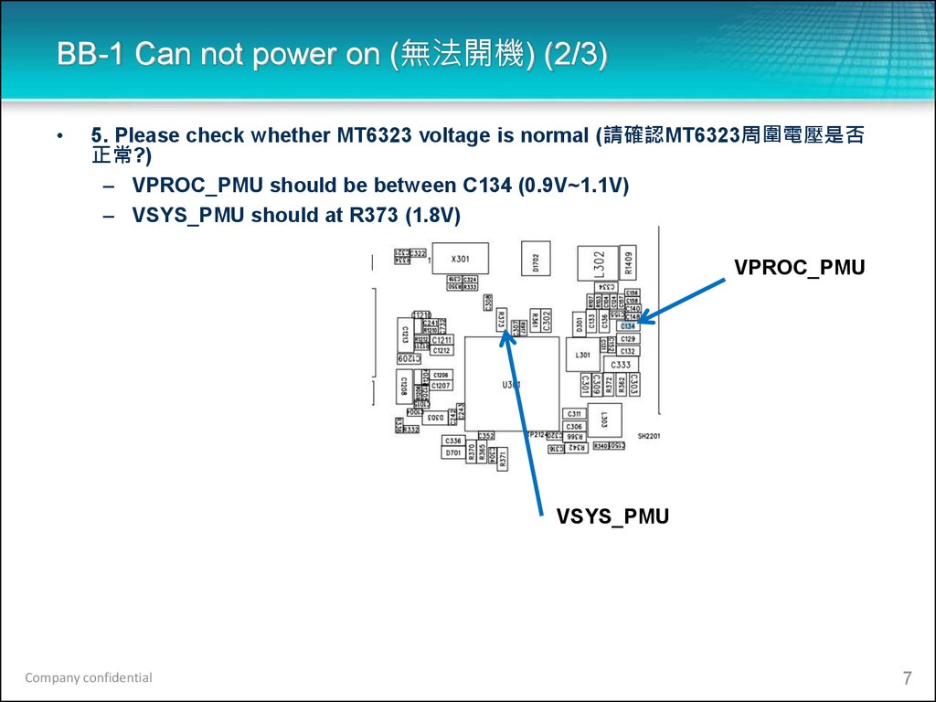
BB-1 Can not power on (無法開機) (2/3)5. Please check whether MT6323 voltage is normal (請確認MT6323周圍電壓是否
正常?)
– VPROC_PMU should be between C134 (0.9V~1.1V)
– VSYS_PMU should at R373 (1.8V)
VPROC_PMU
VSYS_PMU
Company confidential
7
8.
BB-1 Can not power on (無法開機) (3/3)MT6323 Power On/Off sequence
VCORE≈0.7V~1.3V
VPORC≈0.7V~1.3V
VIO18=1.8V
VIO28=2.8V
VM12_INT=1.2V
VA1=2.5V
VA2=2.5V
VUSB=3.3V
VTCXO=2.8V
VMC=3.3V
VMCH=3.3V
RESET=1.8V
Company confidential
8
9.
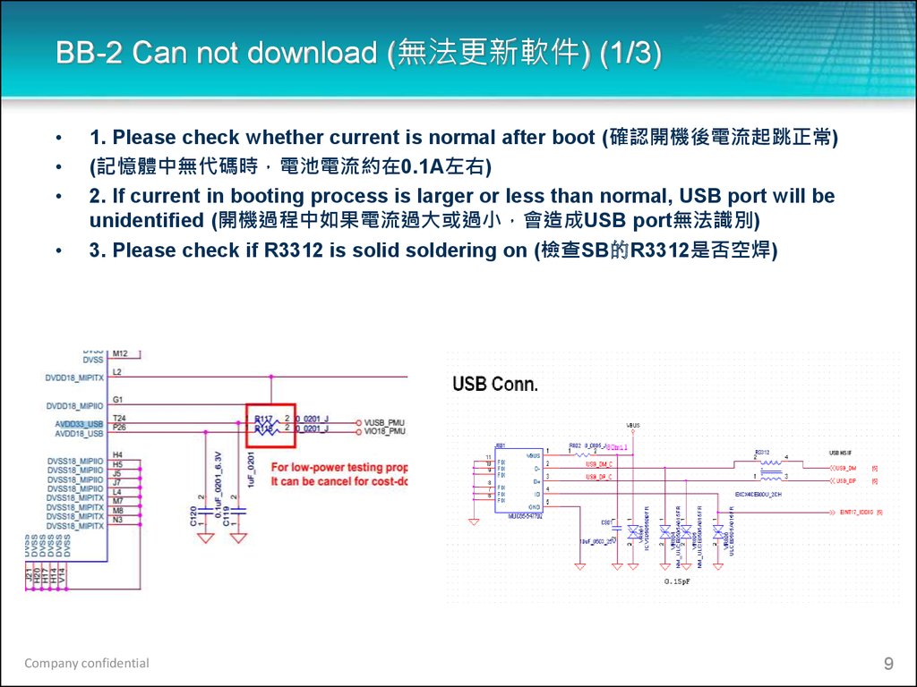
BB-2 Can not download (無法更新軟件) (1/3)1. Please check whether current is normal after boot (確認開機後電流起跳正常)
(記憶體中無代碼時 電池電流約在0.1A左右)
2. If current in booting process is larger or less than normal, USB port will be
unidentified (開機過程中如果電流過大或過小 會造成USB port無法識別)
3. Please check if R3312 is solid soldering on (檢查SB的R3312是否空焊)
Company confidential
9
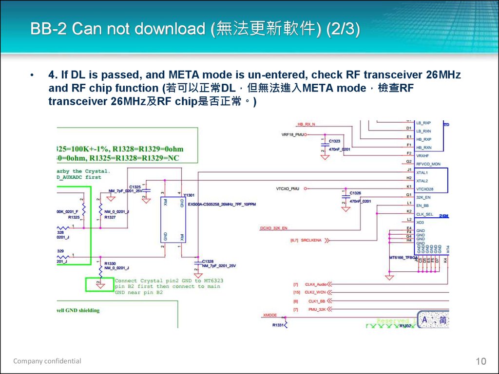
10.
BB-2 Can not download (無法更新軟件) (2/3)4. If DL is passed, and META mode is un-entered, check RF transceiver 26MHz
and RF chip function (若可以正常DL 但無法進入META mode 檢查RF
transceiver 26MHz及RF chip是否正常。)
Company confidential
10
11.
BB-2 Can not download (無法更新軟件) (3/3)5. Check if com port is correct (確認com port是否正確)
Company confidential
11
12.
BB-3 Can not charging (無法充電) (1/2)1. Check if battery resistance R332 Pin1(BAT_ID) is 10kΩ when
battery is installed (確認電池內阻R332 Pin1 (BAT_ID) 當接上電池
後阻抗應該約10kΩ.)
2. Check battery voltage, if 0V reveals open circuit (確認電池電壓
是否為正常 異常為0V (開路))
3. Check if J801 USB connector failure (確認J801 USB connector
是否有異狀?)
Company confidential
12
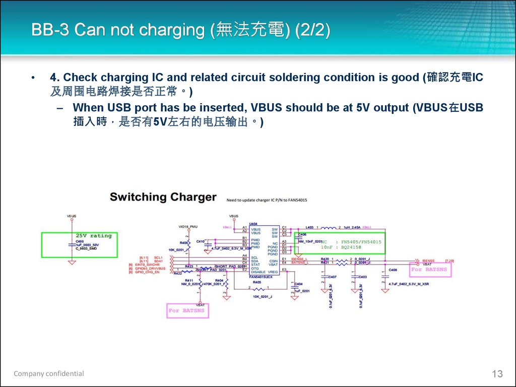
13.
BB-3 Can not charging (無法充電) (2/2)4. Check charging IC and related circuit soldering condition is good (確認充電IC
及周围电路焊接是否正常。)
– When USB port has be inserted, VBUS should be at 5V output (VBUS在USB
插入時 是否有5V左右的电压输出。)
Company confidential
13
14.
BB-4 SIM Card Identification error (SIM卡無法識別) (1/2)1. Check if SIM Card is in normal condition (更換SIM卡 確認卡片是否正常?)
2. Check if J3200 soldering condition is normal (確認J3200吃錫狀況是否正常?)
3. Check SIM related signal SRST, VSIM, SIO and SCLK (確認SIM 相關訊號)
– SRST, VSIM,SIO and SCLK
Company confidential
14
15.
BB-4 SIM Card Identification error (SIM卡無法識別) (2/2)SIM1/SIM2的供电电
压各来自PMU的两
组LDO output
SIM1/SIM2 output
voltage are coming
from two LDO
output of PMU
SIM1和SIM2的
DATA/RST/CLOCK
单独分开使用
DATA/RST/CLOCK
of SIM1 and SIM2
are used
seperately
Company confidential
15
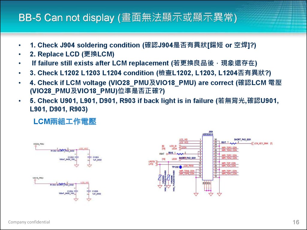
16.
BB-5 Can not display (畫面無法顯示或顯示異常)1. Check J904 soldering condition (確認J904是否有異狀[鍚短 or 空焊]?)
2. Replace LCD (更換LCM)
If failure still exists after LCM replacement (若更換良品後 現象還存在)
3. Check L1202 L1203 L1204 condition (檢查L1202, L1203, L1204否有異狀?)
4. Check if LCM voltage (VIO28_PMU及VIO18_PMU) are correct (確認LCM 電壓
(VIO28_PMU及VIO18_PMU)位準是否正確?)
5. Check U901, L901, D901, R903 if back light is in failure (若無背光,確認U901,
L901, D901, R903)
LCM兩組工作電壓
Company confidential
16
17.
BB-6 sensor function fail (感測器不良) (1/2)所有的sensor都是由I2C總線 中斷信號 電源組成.I2C總線上sensor間會相互影響
所以維修某個 sensor不良時需要同步檢查其他sensor路徑。
All sensors are consisted by I2C bus, interrupt signal and power. Sensors on
I2C bus are affected by each other, therefore related sensors checking is
needed when repairing sensor.
G-sensor供电电压。该电压等同于
VIO18 该电压异常系统就无法开起来
所以sensor不良不用check此电位。
G-Sensor voltage is as same as
VIO18. if this voltage is in error,
system will not boot on. Therefore
it is not necessary to check this
voltage when sensors are on failure
Company confidential
17
18.
BB-6 sensor function fail (感測器不良) (2/2)G-sensor I2C通過上拉電阻連接到CPU 此I2C與touch panel共用
VDD18_PMU異常會造成所有sensor fail。
G-sensor I2C connect to CPU with Pull-up resistor, which share
with touch panel, VDD18_PMU error will lead to all sensors
failure.
Company confidential
18
19.
BB-7 Touch Panel no function (無法觸屏) (1/2)1. Check if TP connector is loosen (確認TP Connector 是否鬆脫?)
2. Replace TP (更換TP)
If failure still exists after TP replacement (若更換後良品後 現象還存在)
3. Check if J2001 is on failure (確認J2001是否有異狀[鍚短 or 空焊]? )
4. Check TB voltage(VDD28_PMU and VDD1V8_PMU) is correct (確認TB 電壓
(VDD28_PMU及VDD1V8_PMU)位準是否正確?)
5. Check control signal of I2C, Reset, INT are correct (確認控制訊號 I2C, Reset,
INT動作是否正常?)
Company confidential
19
20.
BB-7 Touch Panel no function (無法觸屏) (2/2)TP circuit
復位信號
Reset Signal
TP工作電壓
2.8V/1.8V
TP Working
Voltage
2.8v/1.8v
Company confidential
20
21.
BB-8 Vibrator no function (馬達無振動)1. Check if motor is in normal condition (Resistance is 30Ω) (確認馬達是否正常
(馬達阻抗約30Ω))
2. Check if motor soldering condition (確認馬達是否有異狀[鍚短 or 空焊]?)
3. Check if D309 is reversed, C331 soldering condition is good (檢查D309是否反
向 C331焊接是否有异常[鍚短 or 空焊]?)
4. VIBR_PMU voltage is normal when booting (啟動時VIBR_PMU電壓是否正常)
Company confidential
21
22.
BB-9 Camera can not turn on (無法攝像) (1/4)1. Check camera module has been well assembled (確認組裝是否到位?)
2. Replace camera module (更換camera module)
If failure still exists after camera module replaced (若更換後良品後 現象還存在)
3. Check J902 is in normal condition (確認J902是否有異狀[鍚短 or 空焊]? )
4. Check EMI901, EMI902, EMI903 , EMI904, EMI905 soldering condition (確認
EMI901, EMI902, EMI903 , EMI904, EMI905是否有異狀[鍚短 or 空焊]? )
5. Check camera voltage(VCAMD_IO_PMU, VCAMA_PMU, VCAMD_PMU) are
correct (確認Camera 電壓 (VCAMD_IO_PMU, VCAMA_PMU, VCAMD_PMU )位準
是否正確?)
Company confidential
22
23.
BB-9 Camera can not turn on (無法攝像) (2/4)主camera的4組工作電壓均是由PMU LDO輸出通過給camera
All 4 working voltage of main camera are inputted from PMU LDO
Camera
I2C
源頭路徑
Company confidential
23
24.
BB-9 Camera can not turn on (無法攝像) (3/4)1:無法進入拍攝模式,此為camera無法通過I2C信號
被CPU正常識別造成,此不良主要查供電
/reset/CLK/PWD是否正常
1. Camera shooting model is not accessible.
The main cause is camera cannot be identified
by CPU via I2C, need to check power supply for
camera.
2:拍攝黑屏/油畫:此現象為手機進入拍攝模式后,但無
法讀取景物,此類不良主要是camera無法通過DATA
路徑將信號傳給CPU正常處理造成,此類不良主要檢
查camera的DATA。
2. Photos are blurry/black when shooting,
camera is not able to capture scenery after
entering shooting model. The main cause is
camera cannot pass signal to CPU to process
via Data path. Need to check camera DATA path.
Company confidential
24
25.
BB-9 Camera can not turn on (無法攝像) (4/4)VREF/HREF: Sensor垂直/水平參考信號
Sensor reference of horizon and vertical
MCLK: 來自CPU的主時鐘輸出
Main clock from CPU
PCLK: 象數時鐘輸入
Clock input from image-numerology
Company confidential
25
26.
BB-10 MIC no function (麥克風無作用)1. 確認J1003 Microphone是否正常 (正常Mic阻抗約0.95KΩ)
– Check if J1003 Microphone is in normal condition, MIC resistance should
be at 0.95KΩ.
2. 確認MIC 周邊電路是否有異狀[鍚短 or 空焊]?
– Check MIC and related circuit soldering condition.
MIC1
MIC2
Company confidential
26
27.
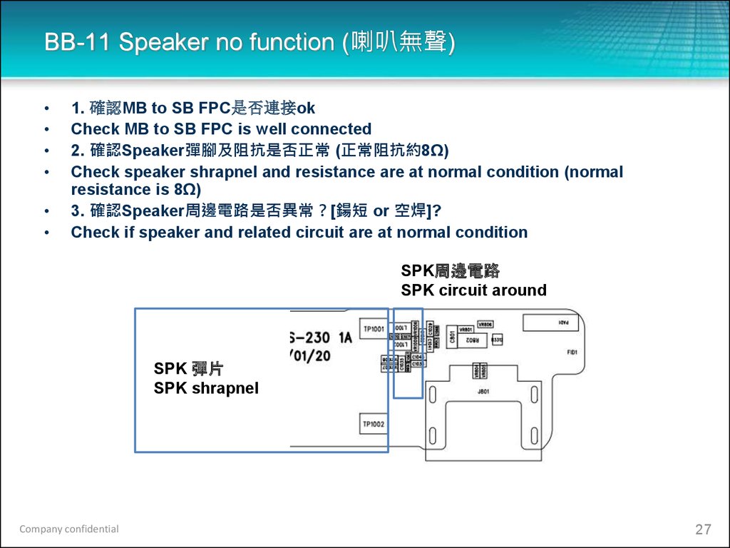
BB-11 Speaker no function (喇叭無聲)1. 確認MB to SB FPC是否連接ok
Check MB to SB FPC is well connected
2. 確認Speaker彈腳及阻抗是否正常 (正常阻抗約8Ω)
Check speaker shrapnel and resistance are at normal condition (normal
resistance is 8Ω)
3. 確認Speaker周邊電路是否異常 [鍚短 or 空焊]?
Check if speaker and related circuit are at normal condition
SPK周邊電路
SPK circuit around
SPK 彈片
SPK shrapnel
Company confidential
27
28.
BB-12 Audio function fail (Audio 不良) (1/4)Audio类不良针对不同测试项fail,检查不同的路径.
1:wave play back fail 测的是SPK路径.
2:receiver fail 测的是手机听筒路径.
3:headset fail 测的是耳机左右声道路径.
4:phone mic1 to headset fail 测的是手机MIC1路径.
5:phone mic1 to headset fail 测的是手机MIC1路径.
6:headsetmic to headset fail 测的是耳机MIC路径.
Check relevant path for different test item failure for Audio error
1:wave play back fail check SPK path
2:receiver fail Check receiver path.
3:headset fail check earphone L/R channel path.
4:phone mic1 to headset fail Check phone MIC1 path.
5:phone mic1 to headset fail Check phone MIC1 path.
6:headsetmic to headset fail Check phone MIC path
Company confidential
28
29.
BB-12 Audio function fail (Audio 不良) (1/4)Speaker path:
PMU給出SPK信號進入Audio PA 進行放大處理
PMU output SPK signal to Audio PA to amplify
Audio PA 輸出放
大后的SPK信號
Audio PA output
SPK signal after
amplifying
Company confidential
29
30.
BB-12 Audio function fail (Audio 不良) (2/4)Receiver path:
聽筒無聲,優先check 0om是否導通
Check 0Com first if receiver is not functional
PMU輸出音頻信號
PMU output audio signal
Phone MIC path
為MIC提供偏置電壓
Provide bias voltage for MIC
MIC信號輸入到
PMU進行音頻處理
MIC signal input
to PMU to
process audio
Company confidential
30
31.
BB-12 Audio function fail (Audio 不良) (3/4)耳機左右聲道電路: Earphone L/R channel circuit
PMU輸出耳機音頻信號
PMU output earphone audio
signal
耳機MIC路徑
Earphone MIC
path
耳機掛機鍵偵測信
號
Earphone dialbutton detection
Company confidential
耳機左右聲道連接至audio jack
Earphone L/R channel link to audio jack
耳機插入偵測PIN
Earphone insert
detection pin
31
32.
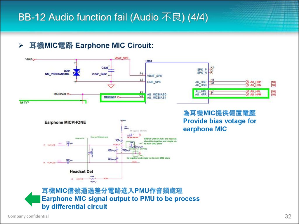
BB-12 Audio function fail (Audio 不良) (4/4)耳機MIC電路 Earphone MIC Circuit:
為耳機MIC提供偏置電壓
Provide bias votage for
earphone MIC
耳機MIC信號通過差分電路進入PMU作音頻處理
Earphone MIC signal output to PMU to be process
by differential circuit
Company confidential
32
33.
BB-13 SD Card no function (SD Card無作用)1. Check SD card is been inserted properly (確認SD CARD有確實卡到位)
2. Check SD card related circuit are in good condition (確認SD Card周邊電路是
否異常 [鍚短 or 空焊]?)
SD card 數據傳輸
Data transmission
SD card 供電端
Power supply
SD card 控制信號
Control signal
SD card 時鐘信號
Clock signal
SD card 偵測信號
SD card signal
detect
針對SD card fail,優先check U1604和
U1605是否空焊導致
CMD/CLK/DET/DATA被中斷
Check U1604 and U1605 soldering
condition first if SD card fail.
Company confidential
33
34.
WIFI/BT/GPSWIFI/BT/GPS 功能使用的IC為MTK MT6627
WIFI/BT/GPS IC are MTK MT6627
I/Q Signal
Connect to CPU
MT6582
SCLK,DataSignal
Company confidential
獨立的26M TCXO Output
Clock to MT6627
Separate 26M TCXO, output
clock to MT6627
34
35.
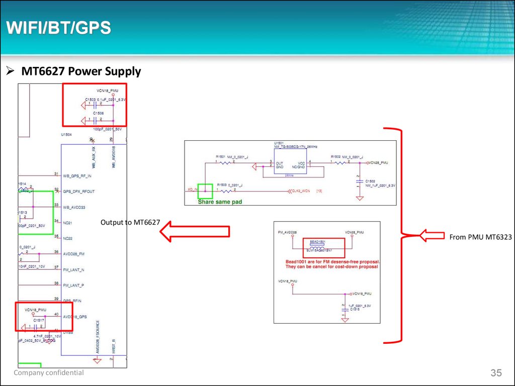
WIFI/BT/GPSMT6627 Power Supply
Output to MT6627
From PMU MT6323
Company confidential
35
36.
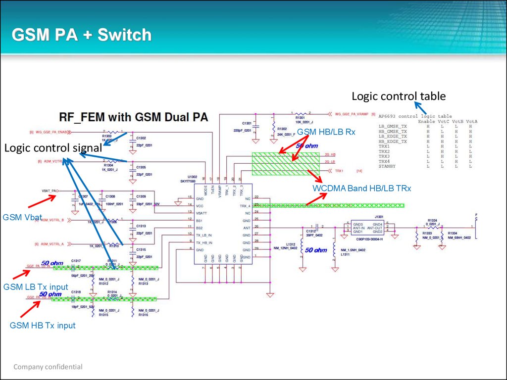
GSM PA + SwitchLogic control table
GSM HB/LB Rx
Logic control signal
WCDMA Band HB/LB TRx
GSM Vbat
GSM LB Tx input
GSM HB Tx input
Company confidential
37.
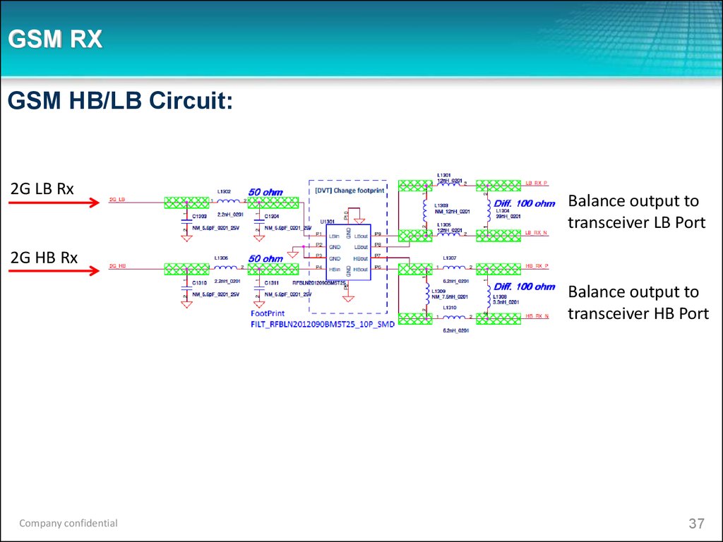
GSM RXGSM HB/LB Circuit:
2G LB Rx
Balance output to
transceiver LB Port
2G HB Rx
Balance output to
transceiver HB Port
Company confidential
37
38.
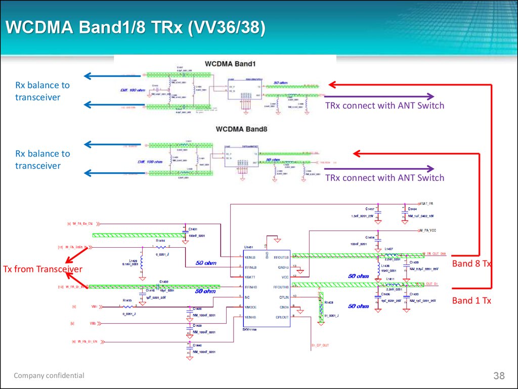
WCDMA Band1/8 TRx (VV36/38)Rx balance to
transceiver
TRx connect with ANT Switch
Rx balance to
transceiver
TRx connect with ANT Switch
Tx from Transceiver
Band 8 Tx
Band 1 Tx
Company confidential
38
39.
WCDMA Band2/5 TRx (VV37)Rx balance to
transceiver
TRx connect with ANT Switch
Rx balance to
transceiver
TRx connect with ANT Switch
Tx from Transceiver
Band 5 Tx
Band 2 Tx
Company confidential
39
40.
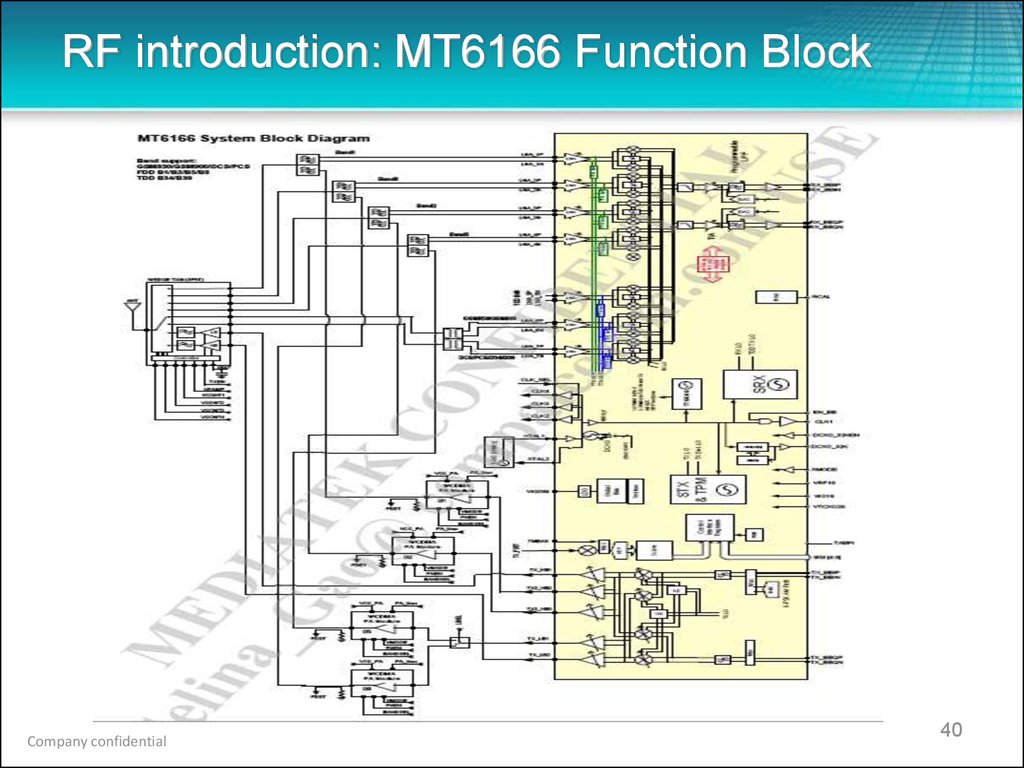
RF introduction: MT6166 Function BlockCompany confidential
40
41.
RF introduction: MT6166 Pin assignmentCompany confidential
41
42.
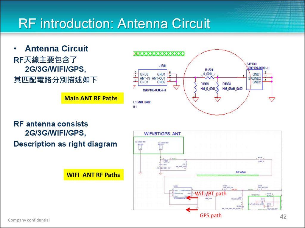
RF introduction: Antenna Circuit• Antenna Circuit
RF天線主要包含了
2G/3G/WIFI/GPS,
其匹配電路分別描述如下
Main ANT RF Paths
RF antenna consists
2G/3G/WIFI/GPS,
Description as right diagram
WIFI ANT RF Paths
Wifi /BT path
Company confidential
GPS path
42
43.
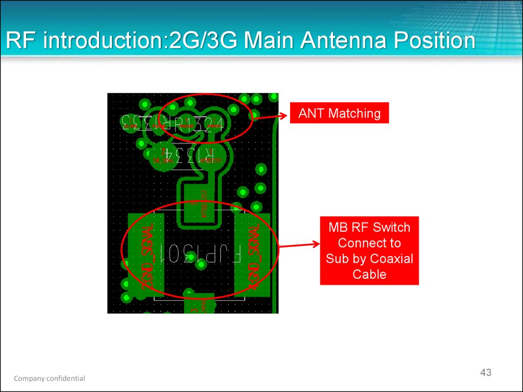
RF introduction:2G/3G Main Antenna PositionANT Matching
MB RF Switch
Connect to
Sub by Coaxial
Cable
Company confidential
43
44.
RF introduction: WIFI Antenna PositionWiFi/BT/GPS
Antenna
Matching
Company confidential
WiFi/BT/GPS
Antenna Clips
44
45.
RF common issueRF-1:Network function error
RF-2:GSM problem
RF-3:WCDMA problem
RF-4:GSM/WCDMA Rx error
RF-5:WIFI problem
45
Company confidential
46.
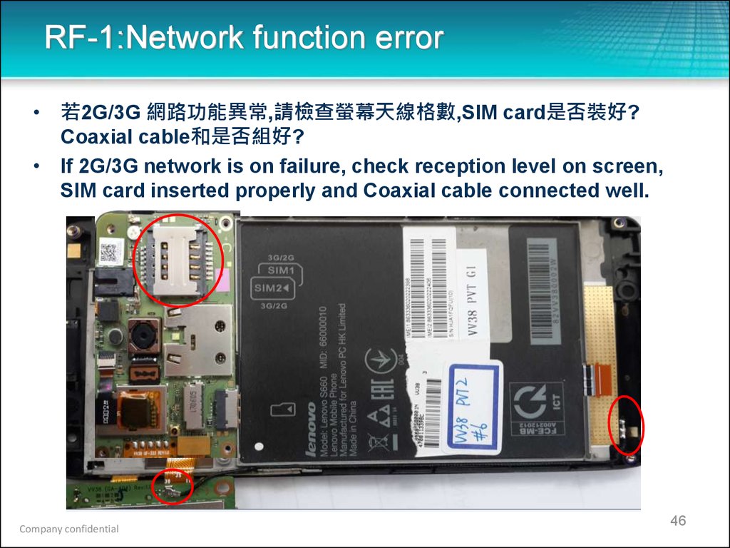
RF-1:Network function error• 若2G/3G 網路功能異常,請檢查螢幕天線格數,SIM card是否裝好?
Coaxial cable和是否組好?
• If 2G/3G network is on failure, check reception level on screen,
SIM card inserted properly and Coaxial cable connected well.
Company confidential
46
47.
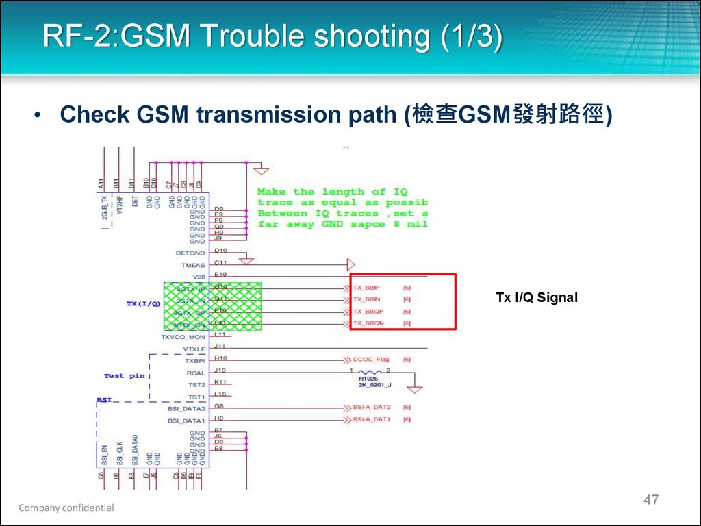
RF-2:GSM Trouble shooting (1/3)• Check GSM transmission path (檢查GSM發射路徑)
Tx I/Q Signal
Company confidential
47
48.
RF-2:GSM Trouble shooting (2/3)GSM發射路徑 GSM transmission path
–
–
–
–
由於2G PA和ASM整合在U1302,檢查發射時對應邏輯控制電壓是否正確
Due to 2G PA and ASM assembly in U1302, check logical control voltage is correct
when transmission testing
使用示波器量測下圖所標腳位的電壓是否符合右下列表
Use oscilloscope test below pins voltage if they match the right bottom table
Company confidential
48
49.
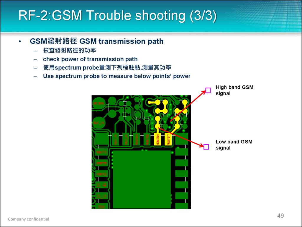
RF-2:GSM Trouble shooting (3/3)GSM發射路徑 GSM transmission path
–
–
–
–
檢查發射路徑的功率
check power of transmission path
使用spectrum probe量測下列標駐點,測量其功率
Use spectrum probe to measure below points’ power
High band GSM
signal
Low band GSM
signal
Company confidential
49
50.
RF-3:WCDMA Trouble shooting (1/5)WCDMA發射路徑 WCDMA transmission path
–
–
–
–
確認IQ路徑
Check IQ path
使用示波器量測下圖所標之腳位,檢視其波形
Use oscilloscope to check below points, check waveform.
Company confidential
50
51.
RF-3:WCDMA Trouble shooting (2/5)WCDMA發射路徑 WCDMA transmission path
–
–
–
–
確認發射路徑
Check signal transmission path
使用频谱仪量測下圖所標之腳位,檢視其Power
Use oscilloscope to test below point and power
Company confidential
51
52.
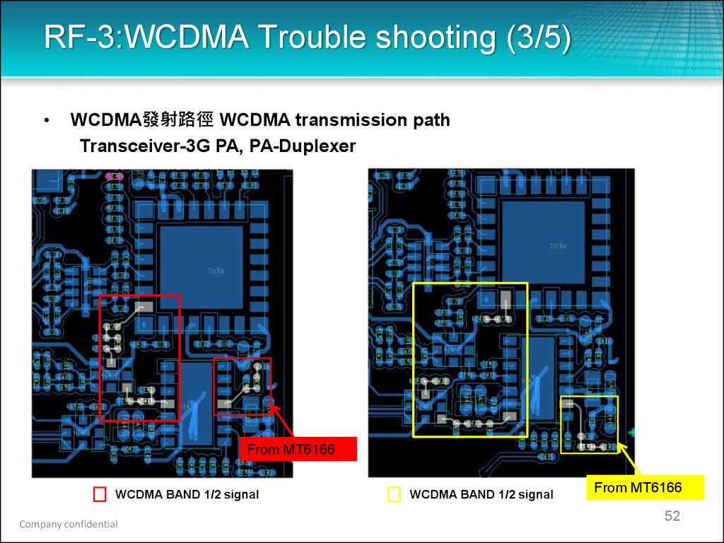
RF-3:WCDMA Trouble shooting (3/5)WCDMA發射路徑 WCDMA transmission path
Transceiver-3G PA, PA-Duplexer
From MT6166
WCDMA BAND 1/2 signal
Company confidential
WCDMA BAND 1/2 signal
From MT6166
52
53.
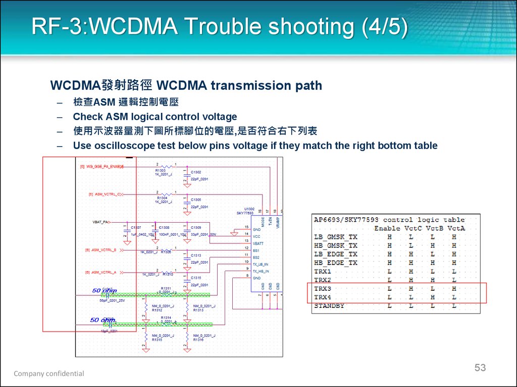
RF-3:WCDMA Trouble shooting (4/5)WCDMA發射路徑 WCDMA transmission path
–
–
–
–
檢查ASM 邏輯控制電壓
Check ASM logical control voltage
使用示波器量測下圖所標腳位的電壓,是否符合右下列表
Use oscilloscope test below pins voltage if they match the right bottom table
Company confidential
53
54.
RF-3:WCDMA Trouble shooting (5/5)發射路徑 ASM-RF Con (GSM + WCDMA)
Transmission Path ASM-RF Con (GSM + WCDMA)
GSM PA+ASM
Company confidential
54
55.
RF-4:GSM/WCDMA Trouble shooting接收路徑 Receiving Path
–
–
–
–
檢查 Antenna switch Module邏輯控制電壓
Check Antenna switch module logical control voltage
使用示波器量測下圖所標腳位的電壓是否符合右下列表
Use oscilloscope test below pins voltage if they match the right bottom table
Company confidential
56.
WIFI/BT/GPSWIFI/BT/GPS IC: MTK MT6627
BT/WIFI:
1. Check whether the antenna of
BT\WIFI damaged
2. Check whether BT\WIFI R1503 has
output frequency of 26M co _ clock
design
3. Check BT\WIFI TRX path
Company confidential
56
57.
WIFI/BT/GPSBT/WIFI TRX path
Co_clock design
MT6166
U1303
MT6627 U1504
Company confidential
MT6627 U1504
57
58.
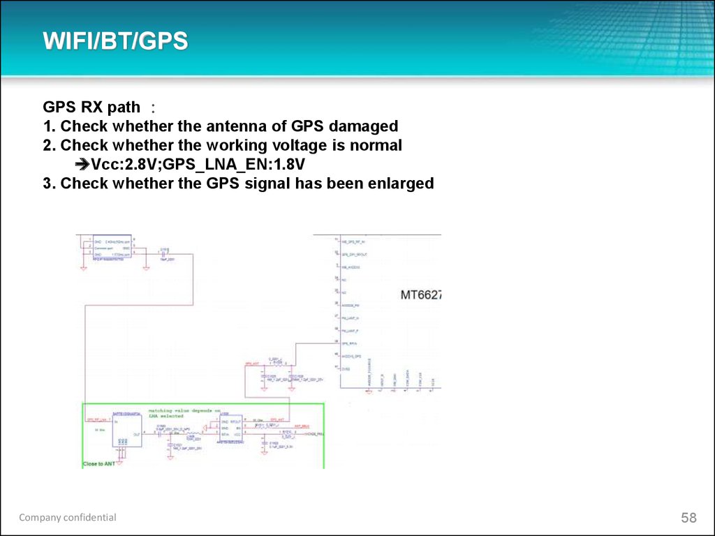
WIFI/BT/GPSGPS RX path
1. Check whether the antenna of GPS damaged
2. Check whether the working voltage is normal
Vcc:2.8V;GPS_LNA_EN:1.8V
3. Check whether the GPS signal has been enlarged
Company confidential
58
59.
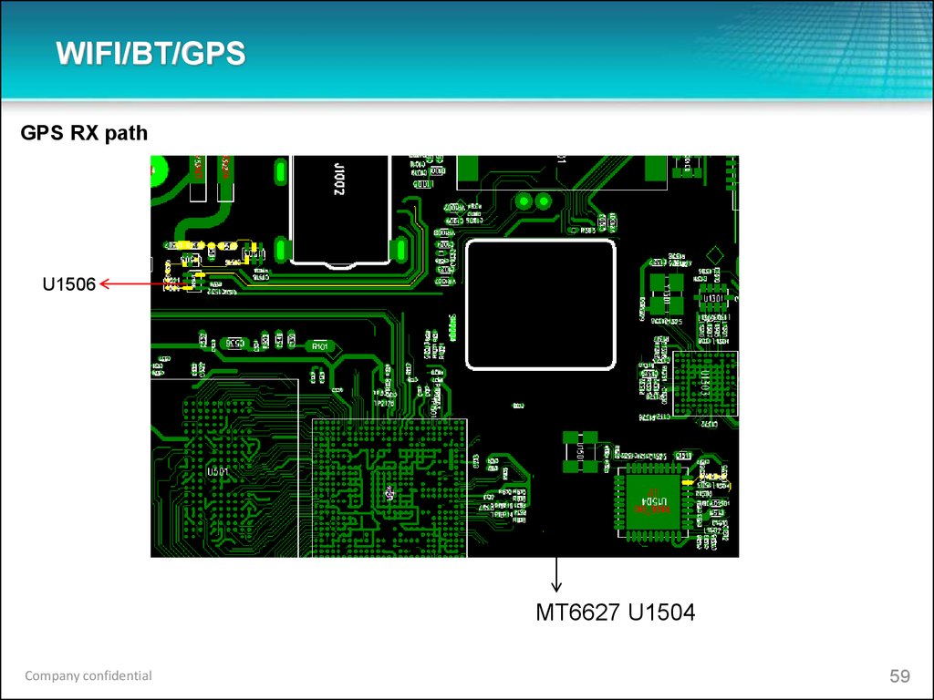
WIFI/BT/GPSGPS RX path
U1506
MT6627 U1504
Company confidential
59
60.
Thank YouCompany confidential
60



























 electronics


