


 informatics
Similar presentations:


Computer Architecture WS 2005-2006
1.
Mic-1: MicroarchitectureUniversity of Fribourg, Switzerland
System I: Introduction to
Computer Architecture
WS 2005-2006
20 December 2006
Béat Hirsbrunner, Amos Brocco, Fulvio Frapolli
<Computer Architecture WS 2006-2007, 20 December 2006> (1)
2.
Mic-1: Microarchitecture (1)<Computer Architecture WS 2005-2006, 20 December 2006> (2)
3.
Mic-1: Microarchitecture (2)Data path
Control section
<Computer Architecture WS 2005-2006, 20 December 2006> (3)
4.
The data pathFrom/
To
Memory
32-bit registers(with exception of
MBR, which is a 8 bit register)
B bus to drive data to
the ALU
C bus to drive data from
the ALU to registers
H register as A-input of
the ALU
ALU with 6 control
signals (and 2 outputs, N to test for Negative
numbers and Z to test for Zero)
<Computer Architecture WS 2005-2006, 20 December 2006> (4)
5.
ALU Control Signals1
<Computer Architecture WS 2005-2006, 20 December 2006> (5)
6.
The data pathRegisters have control signals to enable/disable
reading from them (put value on the B bus) and
writing to them (store value from the C bus)
It is possible to read only from one register at
time: so we can use a 4 -> 16 bit decoder
It is possible to write to one or more registers at
the same time: so we need 9 control signals for
the C bus.
<Computer Architecture WS 2005-2006, 20 December 2006> (6)
7.
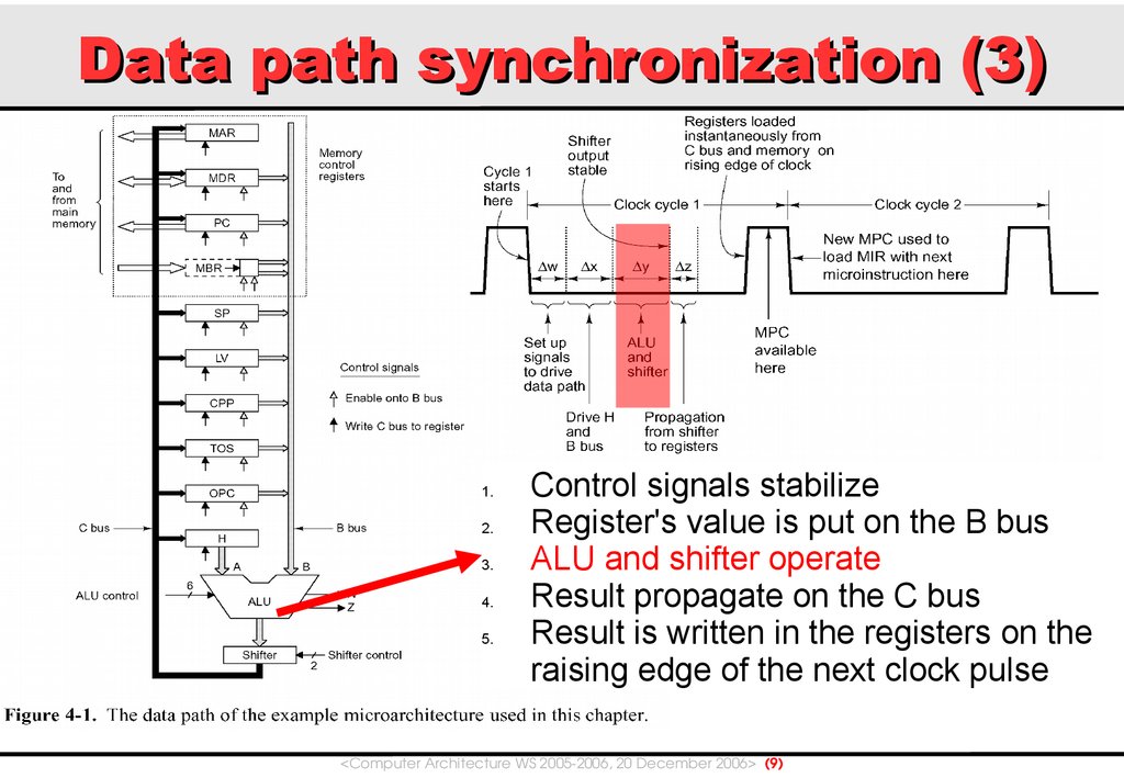
Data path synchronization (1)1.
2.
3.
4.
5.
Control signals stabilize
A register value is put on the B bus
ALU and shifter operate
Result propagate on the C bus
Result is written in the registers on the
raising edge of the next clock pulse
<Computer Architecture WS 2005-2006, 20 December 2006> (7)
8.
Data path synchronization (2)1.
2.
3.
4.
5.
Control signals stabilize
Register's value is put on the B bus
ALU and shifter operate
Result propagate on the C bus
Result is written in the registers on the
raising edge of the next clock pulse
<Computer Architecture WS 2005-2006, 20 December 2006> (8)
9.
Data path synchronization (3)1.
2.
3.
4.
5.
Control signals stabilize
Register's value is put on the B bus
ALU and shifter operate
Result propagate on the C bus
Result is written in the registers on the
raising edge of the next clock pulse
<Computer Architecture WS 2005-2006, 20 December 2006> (9)
10.
Data path synchronization (4)1.
2.
3.
4.
5.
Control signals stabilize
Register's value is put on the B bus
ALU and shifter operate
Result propagate on the C bus
Result is written in the registers on the
raising edge of the next clock pulse
<Computer Architecture WS 2005-2006, 20 December 2006> (10)
11.
Data path synchronization (4)1.
2.
3.
4.
5.
Control signals stabilize
Register's value is put on the B bus
ALU and shifter operate
Result propagate on the C bus
Result is written in the registers on the
raising edge of the next clock pulse
<Computer Architecture WS 2005-2006, 20 December 2006> (11)
12.
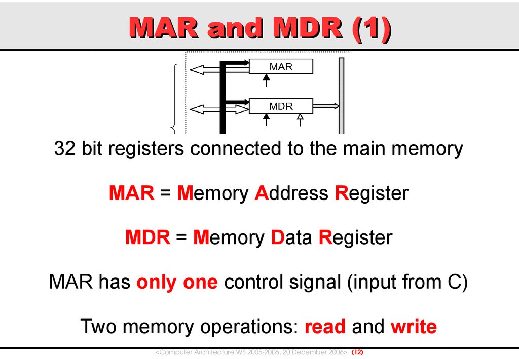
MAR and MDR (1)32 bit registers connected to the main memory
MAR = Memory Address Register
MDR = Memory Data Register
MAR has only one control signal (input from C)
Two memory operations: read and write
<Computer Architecture WS 2005-2006, 20 December 2006> (12)
13.
MAR and MDR (2)Data is word (4*8bit = 32bit in our ISA)
addressed!
=>MAR addresses are shifted 2bit left ( = * 4)
<Computer Architecture WS 2005-2006, 20 December 2006> (13)
14.
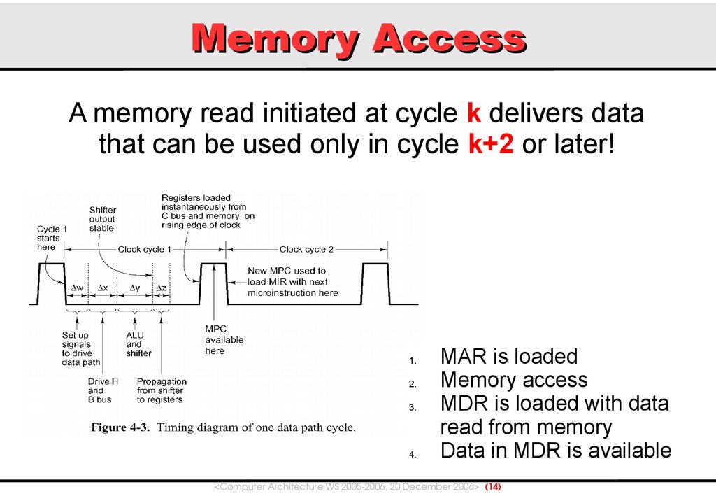
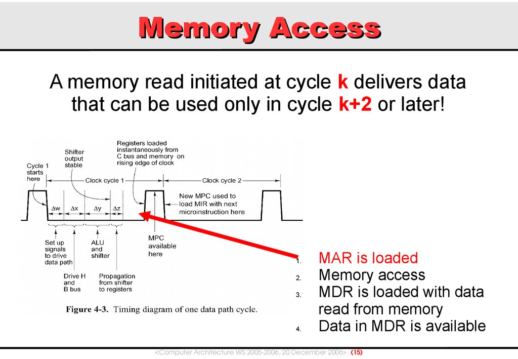
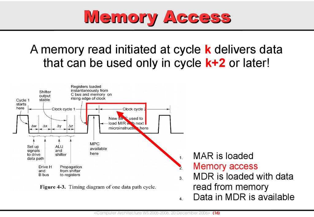
Memory AccessA memory read initiated at cycle k delivers data
that can be used only in cycle k+2 or later!
1.
2.
3.
4.
MAR is loaded
Memory access
MDR is loaded with data
read from memory
Data in MDR is available
<Computer Architecture WS 2005-2006, 20 December 2006> (14)
15.
Memory AccessA memory read initiated at cycle k delivers data
that can be used only in cycle k+2 or later!
1.
2.
3.
4.
MAR is loaded
Memory access
MDR is loaded with data
read from memory
Data in MDR is available
<Computer Architecture WS 2005-2006, 20 December 2006> (15)
16.
Memory AccessA memory read initiated at cycle k delivers data
that can be used only in cycle k+2 or later!
1.
2.
3.
4.
MAR is loaded
Memory access
MDR is loaded with data
read from memory
Data in MDR is available
<Computer Architecture WS 2005-2006, 20 December 2006> (16)
17.
Memory AccessA memory read initiated at cycle k delivers data
that can be used only in cycle k+2 or later!
1.
2.
3.
4.
MAR is loaded
Memory access
MDR is loaded with data
read from memory
Data in MDR is available
<Computer Architecture WS 2005-2006, 20 December 2006> (17)
18.
Memory AccessA memory read initiated at cycle k delivers data
that can be used only in cycle k+2 or later!
< clock cycle 3 >
1.
2.
3.
4.
MAR is loaded
Memory access
MDR is loaded with data
read from memory
Data in MDR is available
<Computer Architecture WS 2005-2006, 20 December 2006> (18)
19.
Memory Access (2)Until start of cycle k+2 the MDR register contains
old data
It is possible to issue consecutive requests, for
example at time k and k+1: corresponding results
will be available at k+2 and k+3
<Computer Architecture WS 2005-2006, 20 December 2006> (19)
20.
PC and MBR8 bit registers connected to the main memory used to read
(fetch) ISA instructions
PC = Program Counter
MBR = Memory Buffer Register
Access also requires one clock cycle (k -> k+2)
MBR has two control signals for the B bus, for signed or
unsigned operations
One memory operation: fetch
<Computer Architecture WS 2005-2006, 20 December 2006> (20)
21.
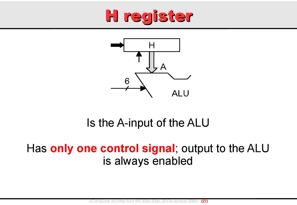
H registerIs the A-input of the ALU
Has only one control signal; output to the ALU
is always enabled
<Computer Architecture WS 2005-2006, 20 December 2006> (21)
22.
ISA, IJVM, MicroarchitectureISA = Instruction Set Architecture
(defines instructions, memory model, available
registers,...)
IJVM = An example ISA (it's stack based
architecture)
The IJVM (Integer Java Virtual Machine) level
executes the IJVM Instruction set
The IJVM is (in this case) implemented by the
Mic-1 Microarchitecture
<Computer Architecture WS 2005-2006, 20 December 2006> (22)
23.
Mic-1 implementationThe Mic-1 is a microprogrammed architecture:
each IJVM instruction (Macroinstruction) is
divided one or more steps.
In each step, a microinstruction is executed by
the Mic-1.
Microinstructions are simpler than ISA
macroinstructions.
<Computer Architecture WS 2005-2006, 20 December 2006> (23)
24.
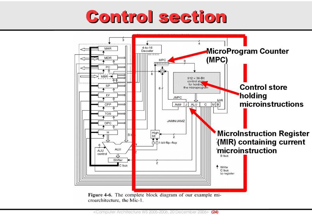
Control sectionMicroProgram Counter
(MPC)
Control store
holding
microinstructions
MicroInstruction Register
(MIR) containing current
microinstruction
<Computer Architecture WS 2005-2006, 20 December 2006> (24)
25.
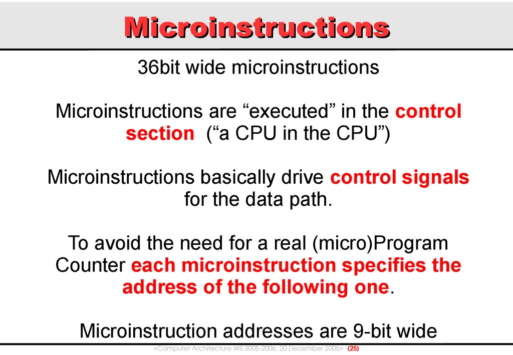
Microinstructions36bit wide microinstructions
Microinstructions are “executed” in the control
section (“a CPU in the CPU”)
Microinstructions basically drive control signals
for the data path.
To avoid the need for a real (micro)Program
Counter each microinstruction specifies the
address of the following one.
Microinstruction addresses are 9-bit wide
<Computer Architecture WS 2005-2006, 20 December 2006> (25)
26.
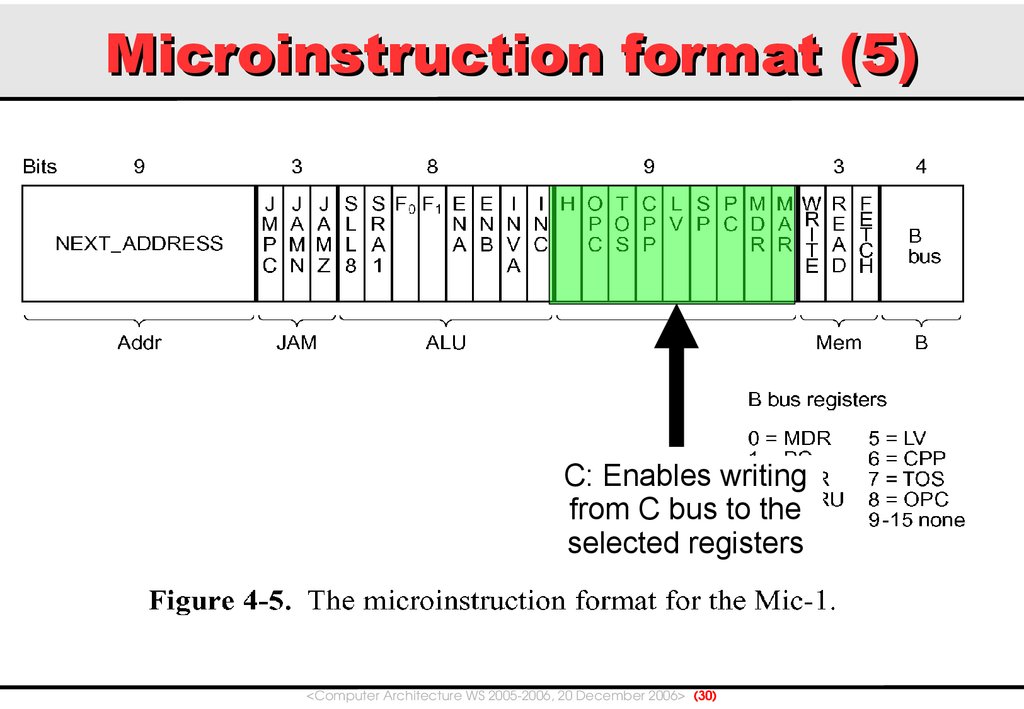
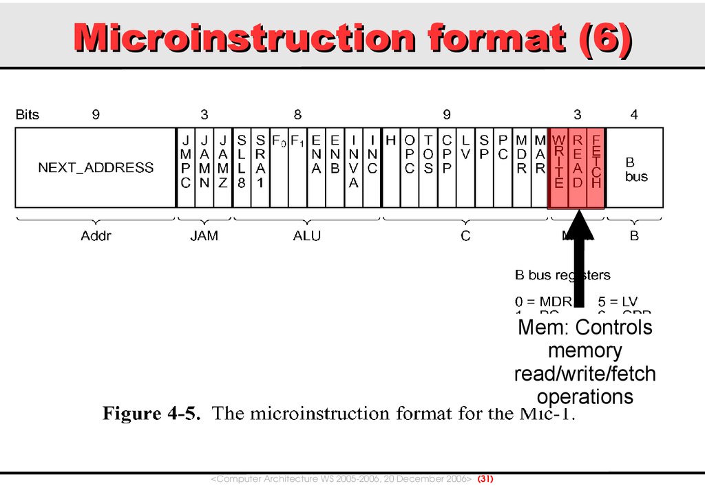
Microinstruction format (1)<Computer Architecture WS 2005-2006, 20 December 2006> (26)
27.
Microinstruction format (2)Addr: Address of the
next
microinstruction
<Computer Architecture WS 2005-2006, 20 December 2006> (27)
28.
Microinstruction format (3)JAM: Determines
how to choose next
microinstruction
<Computer Architecture WS 2005-2006, 20 December 2006> (28)
29.
Microinstruction format (4)ALU: Control
signals to choose
ALU operations
<Computer Architecture WS 2005-2006, 20 December 2006> (29)
30.
Microinstruction format (5)C: Enables writing
from C bus to the
selected registers
<Computer Architecture WS 2005-2006, 20 December 2006> (30)
31.
Microinstruction format (6)Mem: Controls
memory
read/write/fetch
operations
<Computer Architecture WS 2005-2006, 20 December 2006> (31)
32.
Microinstruction format (7)B: Controls which
register can write to
the B bus
<Computer Architecture WS 2005-2006, 20 December 2006> (32)
33.
Driving control signals1.
MIR is loaded on the falling
edge of the clock based on the
MPC address, control signals
propagate
ALU Operation: N and Z values
available and saved
<Computer Architecture WS 2005-2006, 20 December 2006> (33)
34.
Driving control signals1.
MIR is loaded on the falling
edge of the clock based on the
MPC address, control signals
propagate
ALU Operation: N and Z values
available and saved
<Computer Architecture WS 2005-2006, 20 December 2006> (34)
35.
Driving control signals1.
MIR is loaded on the falling
edge of the clock based on the
MPC address, control signals
propagate
ALU Operation: N and Z values
available and saved
<Computer Architecture WS 2005-2006, 20 December 2006> (35)
36.
Next microinstruction (1)Addr (the address of the next
microinstruction coded in the current
microinstruction) is copied in the MPC
(lower 8 bits, high bit is 0)
Addr[8]
If J is 000 the next address is in the MPC
and the next microinstruction can be read
from the control store (Note:
microinstruction are not stored in the same
order as Figure 4-17)
If J is not 000 it is necessary to compute
the next microaddress depending on the
values of J, N and Z (whose value has
been saved in flip-flop because the ALU
returns correct result as long as data is
passing through it)
<Computer Architecture WS 2005-2006, 20 December 2006> (36)
37.
Next microinstruction (2)If JAMN or JAMZ are set to 1, the 'High bit'
function computes the value of the high bit
of the MPC as follows:
F = (JAMZ and Z) or (JAMN and N) or
Addr[8]
(To avoid confusion: Addr[8] is in fact the 9 th bit, the highest, of
Addr, as bits count start from 0)
Addr[8]
So the MPC can assume either the value
of Addr or the value of Addr with the high
bit ORred with 1
<Computer Architecture WS 2005-2006, 20 December 2006> (37)
38.
Next microinstruction (3)F = (JAMZ and Z) or (JAMN and N) or
Addr[8]
An example:
Let Addr <= 0xFF (or we would get the
same value, 0xFF in either case)
Let JAMZ = 1 (or JAMN = 1)
Addr[8]
Let Z=1 (or N=1)
in this case MPC is Addr + 0x100 (for
example: if Addr=0x92, MPC = 0x92 +
Note: 0x100 = 256
<Computer Architecture WS 2005-2006, 20 December 2006> (38)
0x100 = 0x192)
39.
Microinstructions (4)...but why is all that stuff required to determine
the next microinstruction ?
Reason: efficiency
In case of conditional jumps (if..then..else) we normally need two
jump addresses as parameter.
To uniform the microinstruction format we want all instruction to
have the same length: either we make all microinstruction
contain two addresses (-> waste of space) or (better solution) we
specify only one address and compute the second one as Addr +
Constant Value (in Mic-1 Constant Value = 0x100)
<Computer Architecture WS 2005-2006, 20 December 2006> (39)
40.
Next microinstruction (5)If JMPC = 0, Addr is copied to MPC
If JMPC = 1, the lower 8-bits of Addr are
ORred with the MBR value, and the result
is put in the MPC
Normally when JMPC = 1, Addr is set to
either 0x000 or 0x100
Addr[8]
JMPC is used to jump to the address
specified by the MBR, which, as we will
see, contains the opcode of the ISA
instruction: in fact, microinstruction for
each macroinstruction are stored
starting from the position determined by
the opcode of the latter.
<Computer Architecture WS 2005-2006, 20 December 2006> (40)
41.
Next microinstruction (6)Example
ISA instruction:
BIPUSH
opcode is 0x10
corresponding microinstructions starts at
address 0x10 in the control store
Addr[8]
For the reasons explained in the previous
slides, it is clear that the next
microinstruction can be determined only
when the MBR, N and Z are ready, i.e.
starting from the successive clock pulse)
<Computer Architecture WS 2005-2006, 20 December 2006> (41)