Similar presentations:
Clocking for Telecom Infrastructure & Data Center Applications
1. Clocking for Telecom Infrastructure & Data Center Applications
Clocking for Telecom Infrastructure &Data Center Applications
Clock and Timing Solutions
TI Information – Selective Disclosure
1
2. TI clocks for Telecom Infrastructure & Data Center
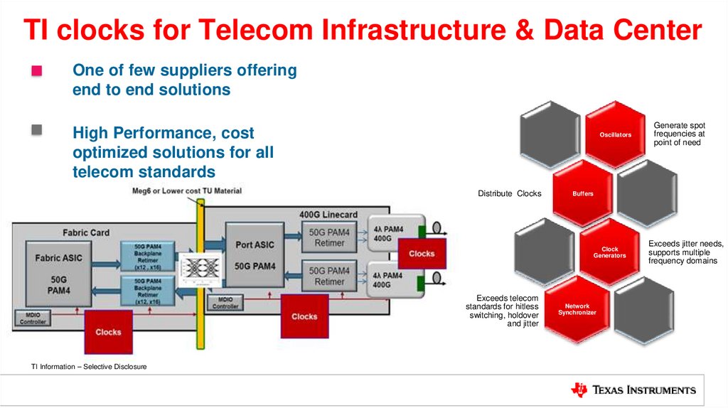
TI clocks for Telecom Infrastructure & Data CenterOne of few suppliers offering
end to end solutions
High Performance, cost
optimized solutions for all
telecom standards
Oscillators
Distribute Clocks
Buffers
Clock
Generators
Exceeds telecom
standards for hitless
switching, holdover
and jitter
TI Information – Selective Disclosure
Generate spot
frequencies at
point of need
Network
Synchronizer
Exceeds jitter needs,
supports multiple
frequency domains
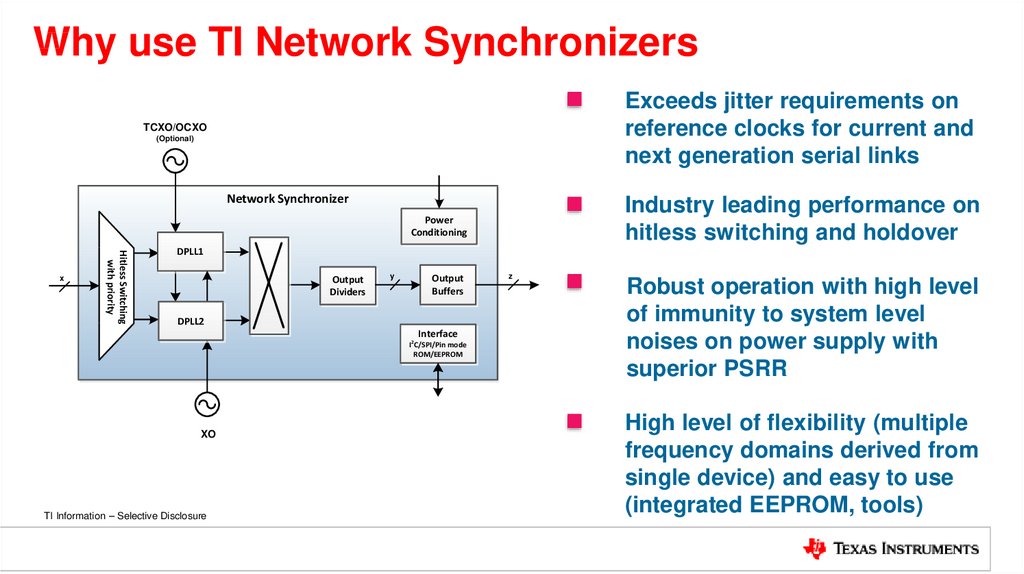
3. Why use TI Network Synchronizers
Exceeds jitter requirements onreference clocks for current and
next generation serial links
TCXO/OCXO
(Optional)
Network Synchronizer
Industry leading performance on
hitless switching and holdover
Power
Conditioning
Hitless Switching
with priority
x
DPLL1
Output
Dividers
y
Output
Buffers
DPLL2
Interface
I2C/SPI/Pin mode
ROM/EEPROM
XO
TI Information – Selective Disclosure
z
Robust operation with high level
of immunity to system level
noises on power supply with
superior PSRR
High level of flexibility (multiple
frequency domains derived from
single device) and easy to use
(integrated EEPROM, tools)
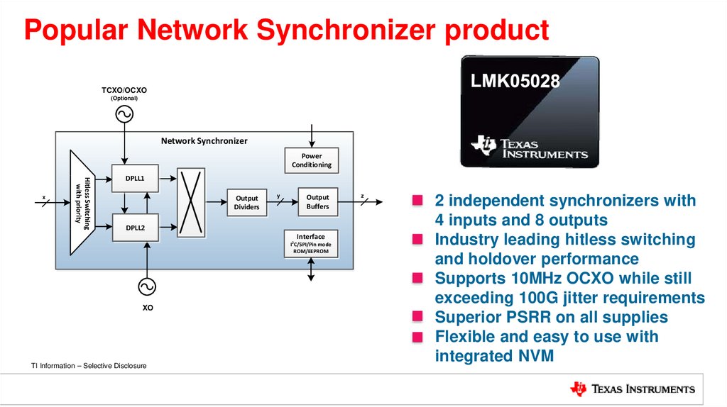
4. Popular Network Synchronizer product
TCXO/OCXO(Optional)
Network Synchronizer
Power
Conditioning
Hitless Switching
with priority
x
DPLL1
Output
Dividers
y
Output
Buffers
DPLL2
Interface
I2C/SPI/Pin mode
ROM/EEPROM
z
XO
TI Information – Selective Disclosure
2 independent synchronizers with
4 inputs and 8 outputs
Industry leading hitless switching
and holdover performance
Supports 10MHz OCXO while still
exceeding 100G jitter requirements
Superior PSRR on all supplies
Flexible and easy to use with
integrated NVM
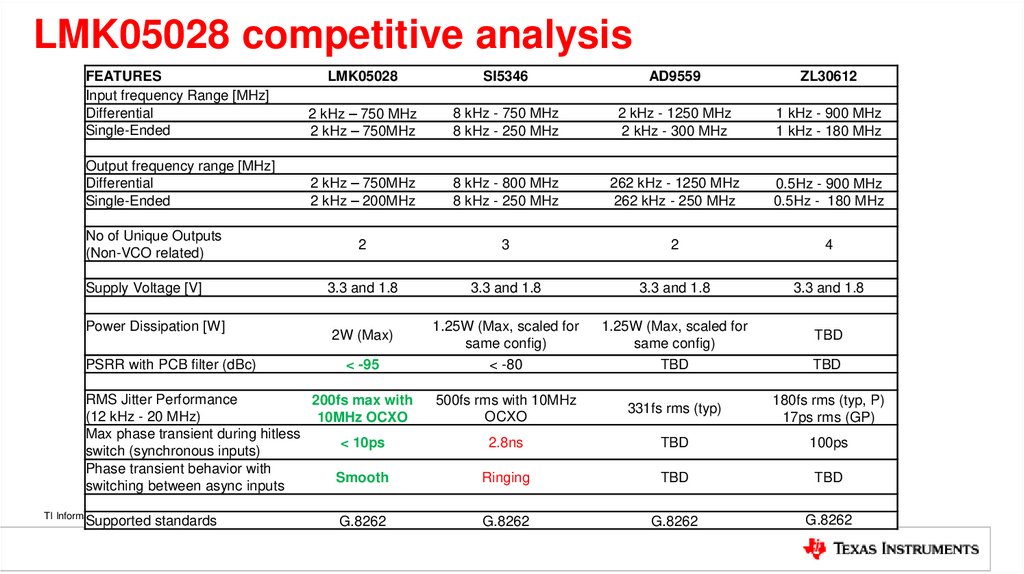
5. LMK05028 competitive analysis
FEATURESInput frequency Range [MHz]
Differential
Single-Ended
LMK05028
SI5346
AD9559
ZL30612
2 kHz – 750 MHz
2 kHz – 750MHz
8 kHz - 750 MHz
8 kHz - 250 MHz
2 kHz - 1250 MHz
2 kHz - 300 MHz
1 kHz - 900 MHz
1 kHz - 180 MHz
Output frequency range [MHz]
Differential
Single-Ended
2 kHz – 750MHz
2 kHz – 200MHz
8 kHz - 800 MHz
8 kHz - 250 MHz
262 kHz - 1250 MHz
262 kHz - 250 MHz
0.5Hz - 900 MHz
0.5Hz - 180 MHz
2
3
2
4
3.3 and 1.8
3.3 and 1.8
3.3 and 1.8
3.3 and 1.8
1.25W (Max, scaled for
same config)
< -80
1.25W (Max, scaled for
same config)
TBD
500fs rms with 10MHz
OCXO
331fs rms (typ)
180fs rms (typ, P)
17ps rms (GP)
2.8ns
TBD
100ps
Ringing
TBD
TBD
G.8262
G.8262
G.8262
No of Unique Outputs
(Non-VCO related)
Supply Voltage [V]
Power Dissipation [W]
PSRR with PCB filter (dBc)
2W (Max)
< -95
RMS Jitter Performance
200fs max with
(12 kHz - 20 MHz)
10MHz OCXO
Max phase transient during hitless
< 10ps
switch (synchronous inputs)
Phase transient behavior with
Smooth
switching between async inputs
TI Information – Selective Disclosure
Supported standards
G.8262
TBD
TBD
6. Why use TI Clock Generators
Exceeds jitter requirements onreference clocks for current and
next generation serial links
Clock generator
Smart MUX
x
PLL1
y
PLL2
Output
Dividers
Output
Buffers
z
Robust operation with high level
of immunity to system level
noises on power supply with
superior PSRR
High level of flexibility (multiple
frequency domains derived from
single device) and easy to use
(integrated EEPROM, tools)
TI Information – Selective Disclosure
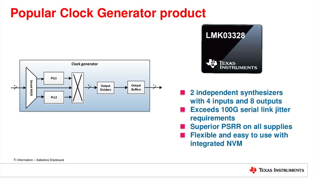
7. Popular Clock Generator product
Clock generatorSmart MUX
x
PLL1
y
PLL2
Output
Dividers
Output
Buffers
z
TI Information – Selective Disclosure
2 independent synthesizers
with 4 inputs and 8 outputs
Exceeds 100G serial link jitter
requirements
Superior PSRR on all supplies
Flexible and easy to use with
integrated NVM
8. LMK03328 Competitive Analysis
Parameter/FeatureDevice control
NVM
Pin mode settings
Flexibility
Frequency Margining
RMS Jitter @156.25 LVPECL fs
25MHz input
Output Types
PSRR (dBc)
Number of Outputs
Operating Conditions oC
Power supply Analog V
Power supply Digital V
Power Dissipation W
Package Type
TI Information – Selective Disclosure
TI LMK03328
I2C, EPROM
Pin mode
Y, 100 writes
Y, 64 states
SI5341
IDT 8T49NS010
I2C, SPI
I2C,Pin mode
Y, 2 writes
N/A
N
Y, 8 states
Low
Limited divider settings
High
High
Fine and Coarse
Coarse
N/A
120
160
120
LVPECL, LVDS, HCSL, LVCMOS
-92
-80
8 outputs (Differential or 10 outputs (Differential or 2x
2x LVCMOS)
LVCMOS)
-40 to 85
3.3
1.8/2.5/3.3
2.25
7mm x 7mm
QFN-48
-40 to 85
3.3
1.8/2.5/3.3
1.14
9mm x 9mm
QFN-64
LVPECL, LVDS
TBD
10 outputs (Differential)
-40 to 85
3.3
3.3
2.57
8mm x 8mm
QFN-56
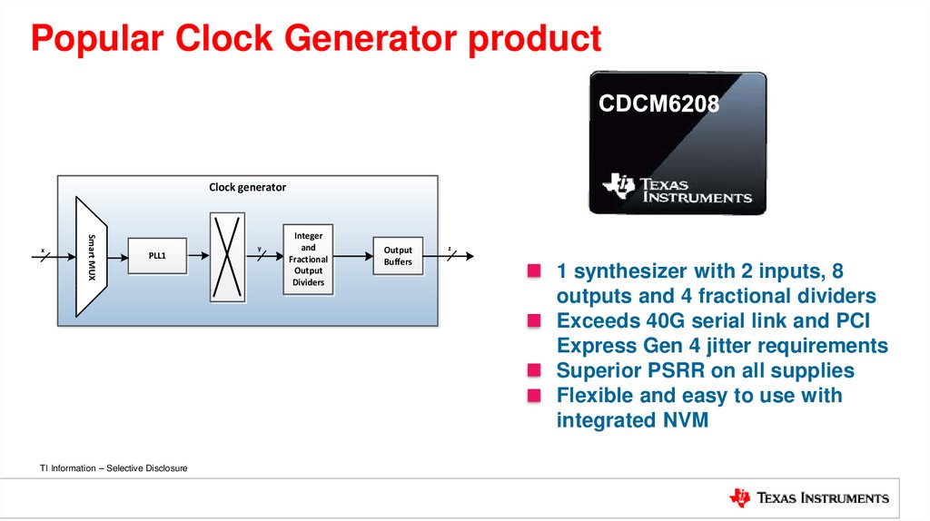
9. Popular Clock Generator product
Clock generatorSmart MUX
x
PLL1
y
Integer
and
Fractional
Output
Dividers
Output
Buffers
z
TI Information – Selective Disclosure
1 synthesizer with 2 inputs, 8
outputs and 4 fractional dividers
Exceeds 40G serial link and PCI
Express Gen 4 jitter requirements
Superior PSRR on all supplies
Flexible and easy to use with
integrated NVM
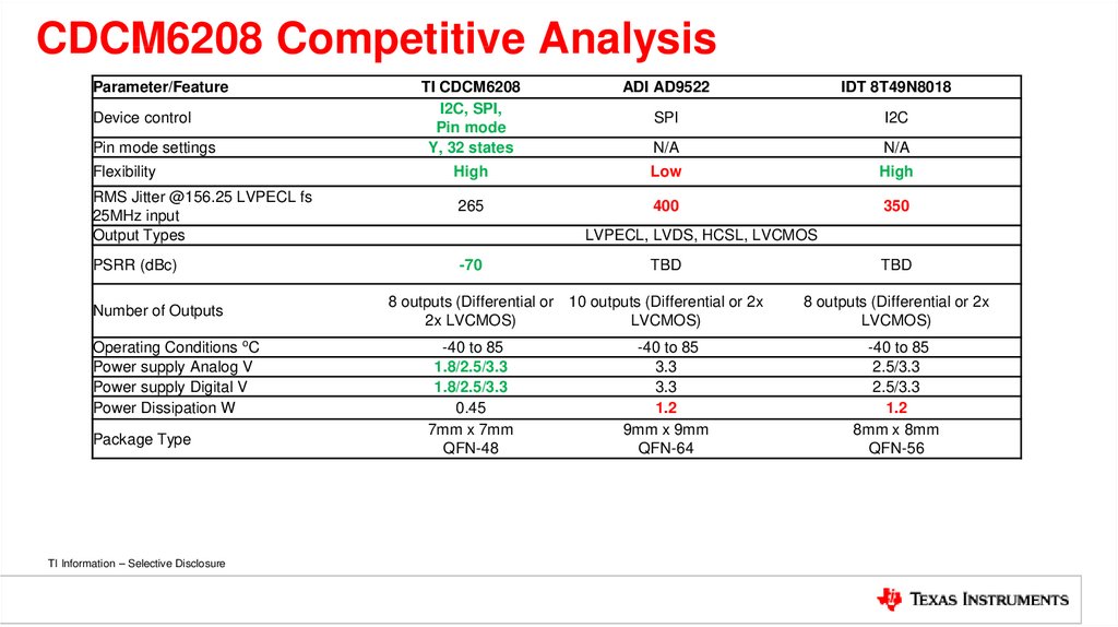
10. CDCM6208 Competitive Analysis
Parameter/FeatureDevice control
Pin mode settings
Flexibility
RMS Jitter @156.25 LVPECL fs
25MHz input
Output Types
PSRR (dBc)
Number of Outputs
Operating Conditions oC
Power supply Analog V
Power supply Digital V
Power Dissipation W
Package Type
TI Information – Selective Disclosure
TI CDCM6208
I2C, SPI,
Pin mode
Y, 32 states
ADI AD9522
IDT 8T49N8018
SPI
I2C
N/A
N/A
High
Low
High
265
400
350
LVPECL, LVDS, HCSL, LVCMOS
-70
TBD
8 outputs (Differential or 10 outputs (Differential or 2x
2x LVCMOS)
LVCMOS)
-40 to 85
1.8/2.5/3.3
1.8/2.5/3.3
0.45
7mm x 7mm
QFN-48
-40 to 85
3.3
3.3
1.2
9mm x 9mm
QFN-64
TBD
8 outputs (Differential or 2x
LVCMOS)
-40 to 85
2.5/3.3
2.5/3.3
1.2
8mm x 8mm
QFN-56
11. Popular Clock Generator product
Clock generatorSmart MUX
x
PLL1
y
Integer
and
Fractional
Output
Dividers
Output
Buffers
z
TI Information – Selective Disclosure
1 synthesizer with 2 inputs, 4
outputs and 4 fractional dividers
Exceeds Express Gen 4 jitter
requirements
Superior PSRR on all supplies
Flexible and easy to use with
integrated NVM
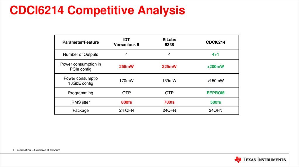
12. CDCI6214 Competitive Analysis
Parameter/FeatureIDT
Versaclock 5
SiLabs
5338
CDCI6214
Number of Outputs
4
4
4+1
Power consumption in
PCIe config
256mW
225mW
<200mW
Power consumptio
10GbE config
170mW
139mW
<150mW
Programming
OTP
OTP
EEPROM
RMS jitter
800fs
700fs
500fs
Package
24 QFN
24QFN
24QFN
TI Information – Selective Disclosure
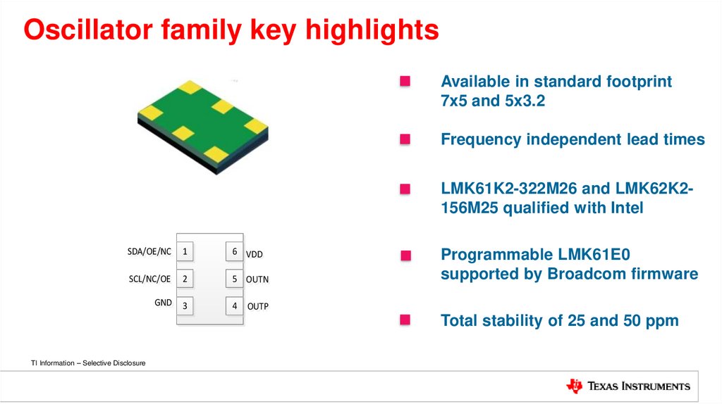
13. Oscillator family key highlights
Available in standard footprint7x5 and 5x3.2
Frequency independent lead times
LMK61K2-322M26 and LMK62K2156M25 qualified with Intel
SDA/OE/NC
SDA/OE/NC 1
6 VDD
VDD
SCL/NC/OE
SCL/NC/OE 2
5 OUTN
OUTN
GND
GND 3
4
Programmable LMK61E0
supported by Broadcom firmware
OUTP
OUTP
Total stability of 25 and 50 ppm
TI Information – Selective Disclosure
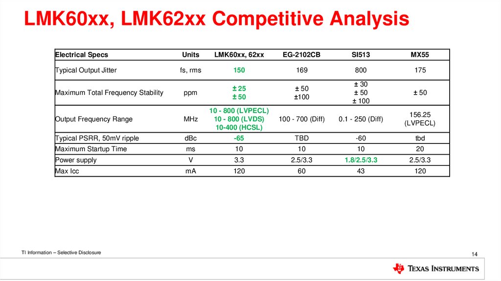
14. LMK60xx, LMK62xx Competitive Analysis
Electrical SpecsUnits
LMK60xx, 62xx
EG-2102CB
SI513
MX55
Typical Output Jitter
fs, rms
150
169
800
175
Maximum Total Frequency Stability
ppm
± 25
± 50
± 50
±100
± 30
± 50
± 100
± 50
Output Frequency Range
MHz
10 - 800 (LVPECL)
10 - 800 (LVDS)
10-400 (HCSL)
100 - 700 (Diff)
0.1 - 250 (Diff)
156.25
(LVPECL)
Typical PSRR, 50mV ripple
dBc
-65
TBD
-60
tbd
Maximum Startup Time
ms
10
10
10
20
V
3.3
2.5/3.3
1.8/2.5/3.3
2.5/3.3
mA
120
60
43
120
Power supply
Max Icc
TI Information – Selective Disclosure
14
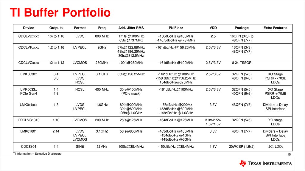
15. TI Buffer Portfolio
DeviceOutputs
Format
Freq
Add. Jitter RMS
PN Floor
VDD
Package
CDCLVDxxxx
1:4 to 1:16
LVDS
800 MHz
171fs @100MHz
65fs @737MHz
-156dBc/Hz @100MHz
-146.5dBc/Hz @ 737MHz
2.5
16QFN (3x3) to
48QFN (7x7)
CDCLVPxxxx
1:2 to 1:16
LVPECL
2GHz
57fs@122.88MHz
48fs@156.25MHz
30fs@312.5MHz
-161dbc/Hz @156.25MHz
2.5V/3.3V
16QFN (3x3)
48QFN (7x7)
CDCLVCxxxx
1:2 to 1:12
LVCMOS
250MHz
100fs@250MHz
-161dBc/Hz @100MHz
2.5V/3.3V
8-24 TSSOP
LMK0030x
3:4
3:8
LVPECL
LVDS
HCSL
3.1 GHz
55fs@156.25MHz
-162 dBc/Hz @100MHz
-158 dBc/Hz@156.25MHz
154dBc/Hz@625MHz
2.5V/3.3V
32QFN (5x5)
40QFN (6x6)
XO Stage
PSRR <-70dB
LDOs
LMK0033x
PCIe Gen4
1:4
1:8
HCSL
400 MHz
30fs@100MHz
(PCIe mask)
-161dBc/Hz@100MHz
2.5V/3.3V
32QFN (5x5)
40QFN (6x6)
XO Stage
PSRR <-70dB
LDOs
LMK0x1xxx
1:8
LVDS
LVPECL
1.6GHz
80fs@200MHz
30fs@800MHz
25fs@1.6GHz
-156dBc/Hz @200Mz
-153dBc/Hz @800MHz
-148dBc/Hz @1.6GHz
3.3V
48QFN (7x7)
Dividers + Delay
SPI Interface
CDCLVC1310
1:10
LVCMOS
200 MHz
25fs@125MHz
-164dBc/Hz @125MHz
3.3V/2.5V/
1.8V/1.5V
32QFN (5x5)
XO stage
LDOs
LMK01801
2:14
LVDS
LVPECL
LVCMOS
3.1GHZ
50fs@800MHz
-163dBc/Hz @100MHz
-154dBc/Hz @1GHz
-148dBc/Hz @3GHz
3.3V
48QFN (7x7)
Dividers + Delay
SPI Interface
LDOs
CDC3S04
1:4
SINE
52MHz
100fs@38.4MHz
-150dBc/Hz @38.4MHz
1.8V
20WCSP (1.6x2)
I2C, LDOs
TI Information – Selective Disclosure
Extra Features
15




 electronics


