


 physics
Similar presentations:


")


")


Plasmonics
1.
Plasmonics• The long wavelength of light (≈ m) creates a problem for
extending optoelectronics into the nanometer regime.
• A possible way out is the conversion of light into plasmons.
• They have much shorter wavelengths than light and are
able to propagate electronic signals.
2.
What is a Plasmon ?A plasmon is a density wave in an electron gas. It is analogous to a
sound wave, which is a density wave in a gas consisting of molecules.
Plasmons exist mainly in metals, where electrons are weakly bound to
the atoms and free to roam. The free electron gas model provides a
good approximation (also known as jellium model).
The electrons in a metal can wobble like a piece of jelly, pulled back by
the attraction of the positive metal ions that they leave behind.
In contrast to the single electron wave function that we encountered
already, a plasmon is a collective wave where billions of electrons oscillate in sync.
3.
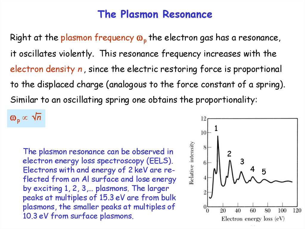
The Plasmon ResonanceRight at the plasmon frequency p the electron gas has a resonance,
it oscillates violently. This resonance frequency increases with the
electron density n , since the electric restoring force is proportional
to the displaced charge (analogous to the force constant of a spring).
Similar to an oscillating spring one obtains the proportionality:
p n
The plasmon resonance can be observed in
electron energy loss spectroscopy (EELS).
Electrons with and energy of 2 keV are reflected from an Al surface and lose energy
by exciting 1, 2, 3,… plasmons. The larger
peaks at multiples of 15.3 eV are from bulk
plasmons, the smaller peaks at multiples of
10.3 eV from surface plasmons.
1
2
3
4 5
4.
Why are Metals Shiny ?An electric field cannot exist inside a metal, because metal electrons
react to it by creating an opposing screening field (Lect. 2, Slide 13).
An example is the image charge, which exactly cancels the field of any
external charge. This is also true for an electromagnetic wave, where
electrons respond to the changing external field and screen it at any
given time. As a result, the electromagnetic wave cannot enter a metal
and gets reflected back out.
However, at high frequency (= high photon energy) there comes a point
when the external field oscillates too fast for the electrons to follow.
Beyond this frequency a metal loses its reflectivity. The corresponding
energy is the plasmon energy
Ep = ħ p (typically 10-30 eV,
deep into the ultraviolet).
The reflectivity of aluminum
cuts off at its plasmon energy
Data (dashed) are compared
to the electron gas model (full).
Ep
5.
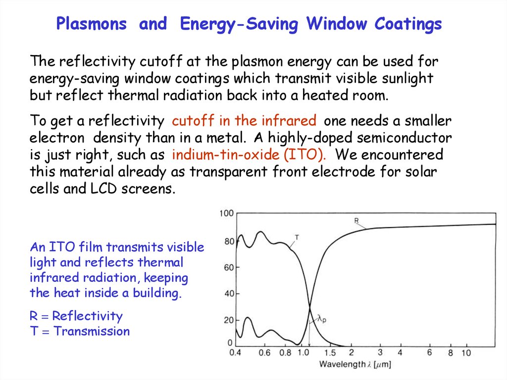
Plasmons and Energy-Saving Window CoatingsThe reflectivity cutoff at the plasmon energy can be used for
energy-saving window coatings which transmit visible sunlight
but reflect thermal radiation back into a heated room.
To get a reflectivity cutoff in the infrared one needs a smaller
electron density than in a metal. A highly-doped semiconductor
is just right, such as indium-tin-oxide (ITO). We encountered
this material already as transparent front electrode for solar
cells and LCD screens.
An ITO film transmits visible
light and reflects thermal
infrared radiation, keeping
the heat inside a building.
R = Reflectivity
T = Transmission
6.
Low-Dimensional Plasmons in NanostructuresLecture 8 showed how single electron waves become quantized by
confinement in a nanostructure. Likewise, collective electron waves
(= plasmons) are affected by the boundary conditions in a thin film,
a nano-rod, or a nano-particle.
Plasmons in metal nanoparticles are often called Mie-resonances,
after Gustav Mie who calculated them hundred years ago. Their
resonance energy and color depend strongly on their size, similar
to the color change induced in semiconductor nanoparticles by
confinement of single electrons (Lecture 9, Slides 6,7). In both
cases, smaller particles have higher resonance energy (blue shift).
7.
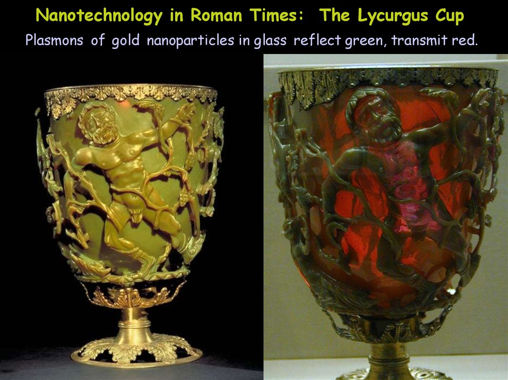
Nanotechnology in Roman Times: The Lycurgus CupPlasmons of gold nanoparticles in glass reflect green, transmit red.
8.
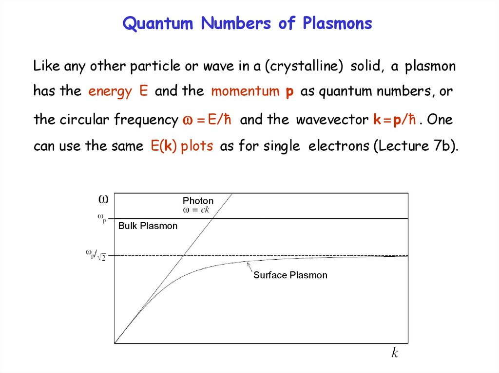
Quantum Numbers of PlasmonsLike any other particle or wave in a (crystalline) solid, a plasmon
has the energy E and the momentum p as quantum numbers, or
the circular frequency = E/ħ and the wavevector k = p/ħ . One
can use the same E(k) plots as for single electrons (Lecture 7b).
Photon
Bulk Plasmon
Surface Plasmon
9.
Coupling of Light and PlasmonsTo combine optoelectronics with plasmonics one has to convert
light (photons) into plasmons. This is not as simple as it sounds.
Bulk plasmons are longitudinal oscillations (parallel to the propa-
gation direction), while photons are transverse (perpendicular to
the propagation). They don’t match.
Surface plasmons are transverse, but they are mismatched to
photons in their momentum. The two E(k) curves never cross.
It is possible to provide the necessary momentum by a grating,
which transmits the wavevector k = 2 /d (d = line spacing) .
10.
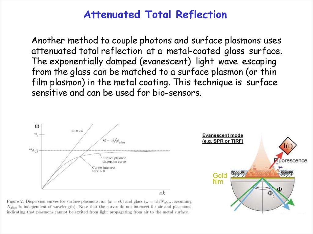
Attenuated Total ReflectionAnother method to couple photons and surface plasmons uses
attenuated total reflection at a metal-coated glass surface.
The exponentially damped (evanescent) light wave escaping
from the glass can be matched to a surface plasmon (or thin
film plasmon) in the metal coating. This technique is surface
sensitive and can be used for bio-sensors.
Gold
film
11.
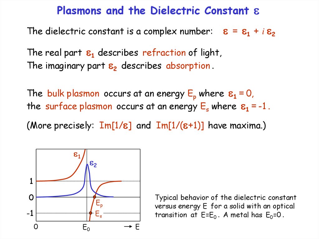
Plasmons and the Dielectric ConstantThe dielectric constant is a complex number:
= 1 + i 2
The real part 1 describes refraction of light,
The imaginary part 2 describes absorption .
The bulk plasmon occurs at an energy Ep where 1 = 0,
the surface plasmon occurs at an energy Es where 1 = -1 .
(More precisely: Im[1/ ] and Im[1/( +1)] have maxima.)
1
2
1
0
Typical behavior of the dielectric constant
versus energy E for a solid with an optical
transition at E=E0 . A metal has E0=0 .
Ep
-1
Es
0
E0
E
12.
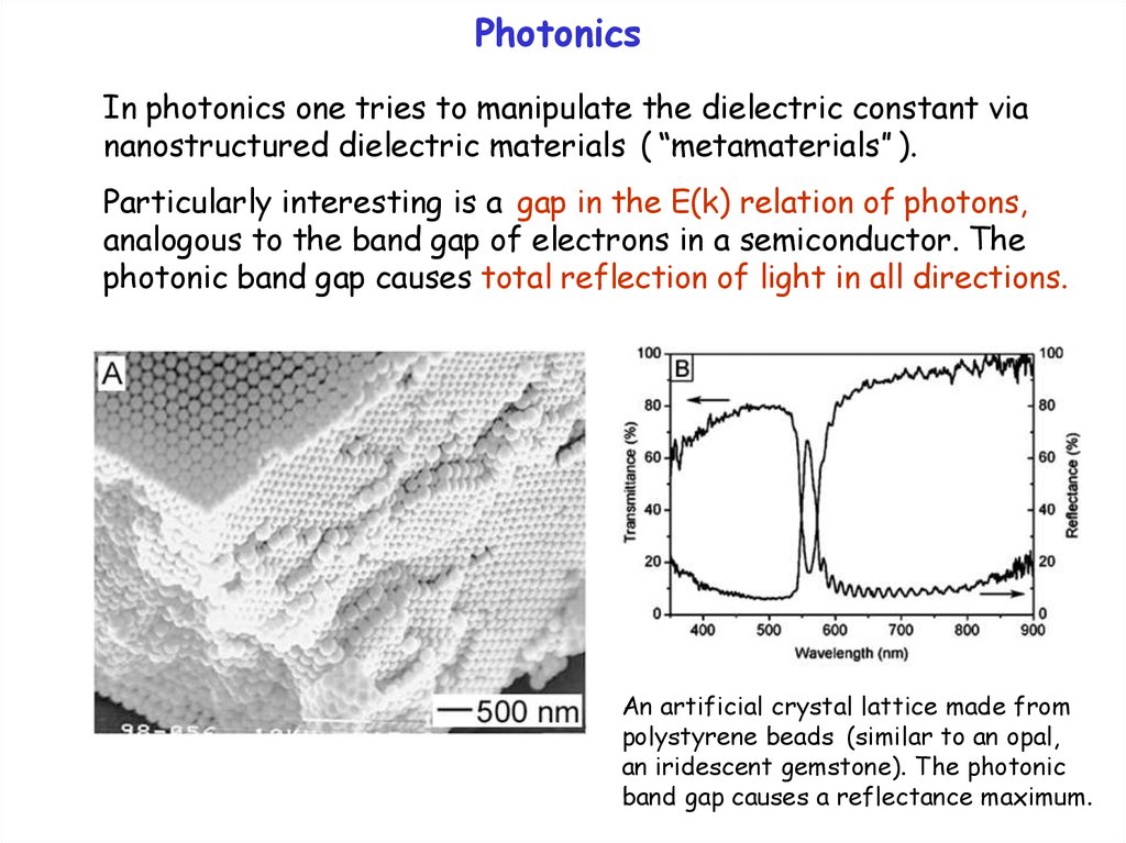
PhotonicsIn photonics one tries to manipulate the dielectric constant via
nanostructured dielectric materials ( “metamaterials” ).
Particularly interesting is a gap in the E(k) relation of photons,
analogous to the band gap of electrons in a semiconductor. The
photonic band gap causes total reflection of light in all directions.
An artificial crystal lattice made from
polystyrene beads (similar to an opal,
an iridescent gemstone). The photonic
band gap causes a reflectance maximum.
13.
Cloaking: Making an Object InvisibleSurrounding an object with a material having the right kind of
dielectric properties (negative refractive index) can make the
object invisible.
A
B
Cloaking simulation in two dimensions:
A. The black disc blocks the light coming from the left and reflects it back,
leaving a shadow towards the right (green/yellow).
B. The surrounding ring of cloaking material guides the light around the disc
and thereby fills in the shadow.
14.
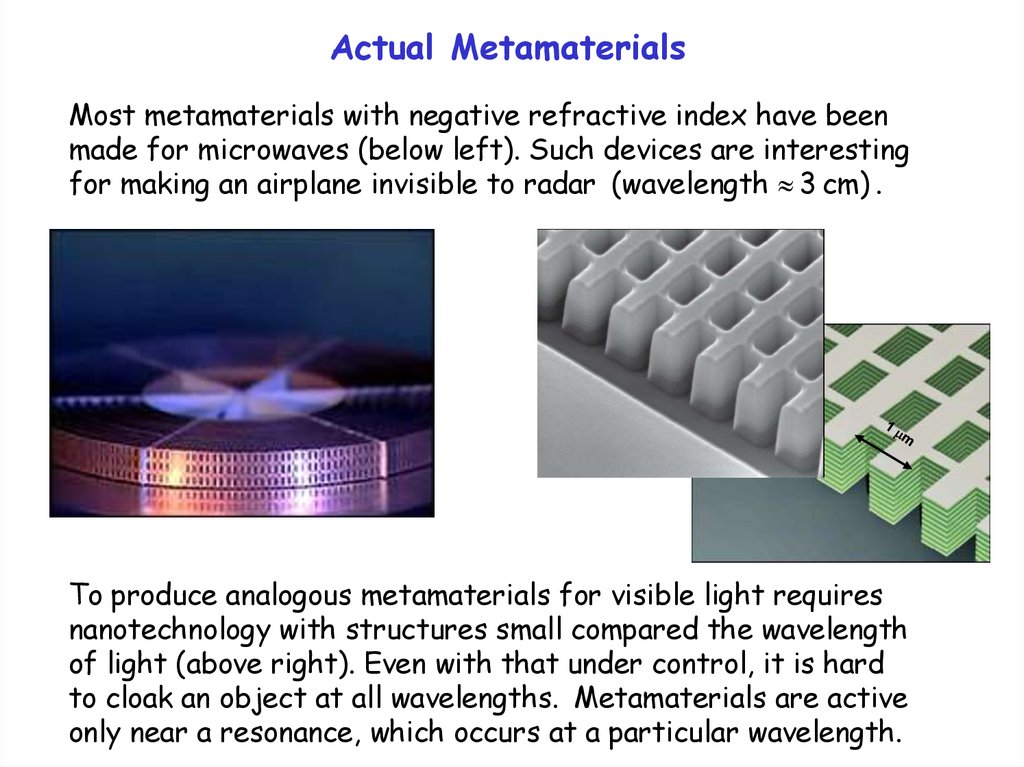
Actual MetamaterialsMost metamaterials with negative refractive index have been
made for microwaves (below left). Such devices are interesting
for making an airplane invisible to radar (wavelength 3 cm) .
To produce analogous metamaterials for visible light requires
nanotechnology with structures small compared the wavelength
of light (above right). Even with that under control, it is hard
to cloak an object at all wavelengths. Metamaterials are active
only near a resonance, which occurs at a particular wavelength.
15.
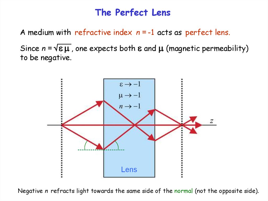
The Perfect LensA medium with refractive index n = -1 acts as perfect lens.
Since n = , one expects both and (magnetic permeability)
to be negative.
Lens
Negative n refracts light towards the same side of the normal (not the opposite side).