


 electronics
Similar presentations:
")


")


Semi conductor’s (lecture 2 - 1)
1.
Semiconductor’sPhysics
Lecture #1
Introduction. Semiconductors. Classification of Materials by Specific Electrical Conductivity
2.
Introduction to Semiconductors• Semiconductors are materials with electrical conductivity between conductors and
insulators.
• They are the foundation of modern electronics, used in devices like diodes, transistors, and
integrated circuits.
•Semiconductors are usually made from elements in Group IV of
the periodic table, like silicon (Si) and germanium (Ge).
•Their atomic structure allows for the creation of free charge
carriers (electrons and holes) under certain conditions.
•Covalent Bonds: Electrons shared between atoms.
•Band Gap: Energy difference between the valence band and
conduction band.
3.
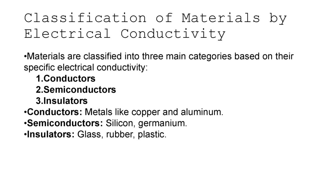
Classification of Materials byElectrical Conductivity
•Materials are classified into three main categories based on their
specific electrical conductivity:
1.Conductors
2.Semiconductors
3.Insulators
•Conductors: Metals like copper and aluminum.
•Semiconductors: Silicon, germanium.
•Insulators: Glass, rubber, plastic.
4.
Applications of Semiconductors•Semiconductors are essential in modern
technology:
•Diodes: Allow current to flow in one direction.
•Transistors: Act as switches or amplifiers.
•Integrated Circuits: Combine many
semiconductors in one chip.
•Importance in computers, smartphones, solar cells.
5.
A list of the main definitions and core elements insemiconductor physics
1. Semiconductor
• Definition: A material that has an electrical conductivity between that of a conductor and an insulator. Its conductivity can be altered by introducing impurities
(doping) or by applying an external electric field.
• Examples: Silicon (Si), Germanium (Ge), Gallium Arsenide (GaAs).
2. Band Theory of Solids
• Conduction Band: The range of electron energy levels in a solid where electrons can move freely and contribute to conduction.
• Valence Band: The energy band in a solid where electrons are bound to atoms and are not free to move.
• Band Gap: The energy difference between the conduction band and the valence band. It determines the electrical conductivity of the material.
3. Intrinsic Semiconductor
• Definition: A pure semiconductor material without any significant doping. The number of charge carriers (electrons and holes) is generated by thermal excitation.
• Example: Pure silicon.
4. Extrinsic Semiconductor
• Definition: A semiconductor that has been doped with impurities to alter its electrical properties. Doping introduces additional charge carriers.
• Types:
n-type Semiconductor: Doped with donor atoms that have more valence electrons than the semiconductor, resulting in more free electrons.
p-type Semiconductor: Doped with acceptor atoms that have fewer valence electrons, creating more holes.
6.
A list of the main definitions and core elements insemiconductor physics
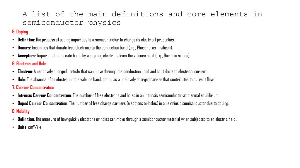
5. Doping
• Definition: The process of adding impurities to a semiconductor to change its electrical properties.
• Donors: Impurities that donate free electrons to the conduction band (e.g., Phosphorus in silicon).
• Acceptors: Impurities that create holes by accepting electrons from the valence band (e.g., Boron in silicon).
6. Electron and Hole
• Electron: A negatively charged particle that can move through the conduction band and contribute to electrical current.
• Hole: The absence of an electron in the valence band, acting as a positively charged carrier that contributes to current flow.
7. Carrier Concentration
• Intrinsic Carrier Concentration: The number of free electrons and holes in an intrinsic semiconductor at thermal equilibrium.
• Doped Carrier Concentration: The number of free charge carriers (electrons or holes) in an extrinsic semiconductor due to doping.
8. Mobility
• Definition: The measure of how quickly electrons or holes can move through a semiconductor material when subjected to an electric field.
• Units: cm²/V·s
7.
A list of the main definitions and core elements insemiconductor physics
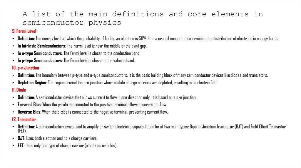
9. Fermi Level
• Definition: The energy level at which the probability of finding an electron is 50%. It is a crucial concept in determining the distribution of electrons in energy bands.
• In Intrinsic Semiconductors: The Fermi level is near the middle of the band gap.
• In n-type Semiconductors: The Fermi level is closer to the conduction band.
• In p-type Semiconductors: The Fermi level is closer to the valence band.
10. p-n Junction
• Definition: The boundary between p-type and n-type semiconductors. It is the basic building block of many semiconductor devices like diodes and transistors.
• Depletion Region: The region around the p-n junction where mobile charge carriers are depleted, resulting in an electric field.
11. Diode
• Definition: A semiconductor device that allows current to flow in one direction only. It is based on a p-n junction.
• Forward Bias: When the p-side is connected to the positive terminal, allowing current to flow.
• Reverse Bias: When the p-side is connected to the negative terminal, preventing current flow.
12. Transistor
• Definition: A semiconductor device used to amplify or switch electronic signals. It can be of two main types: Bipolar Junction Transistor (BJT) and Field Effect Transistor
(FET).
• BJT: Uses both electron and hole charge carriers.
• FET: Uses only one type of charge carrier (electrons or holes).
8.
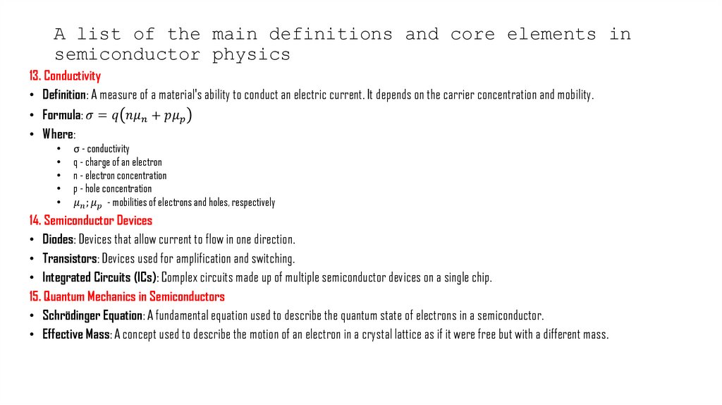
A list of the main definitions and core elements insemiconductor physics
13. Conductivity
• Definition: A measure of a material's ability to conduct an electric current. It depends on the carrier concentration and mobility.
• Formula: