


")
 и нанесения резиста (Sawatec)")
")


 (США, Arizona State University): results of simulation")

 vs. electron energy E")


 high performance")
 low power")


")
 => no realism")

")


")


 electronics
Similar presentations:
. Junction field-effect transistor (JFET)")


Приборы полупроводниковой микро- и наноэлектроники
1.
Приборы полупроводниковой микро- инаноэлектроники
В.В. Вьюрков – лектор, зам. зав. кафедрой
Факультет физической и квантовой электроники (ФФКЭ МФТИ)
Физико-технологический институт
Российской академии наук
2. План лекций
Технология наноэлектронныхприборов
Теория наноэлектронных
приборов
Квантовые компьютеры
3.
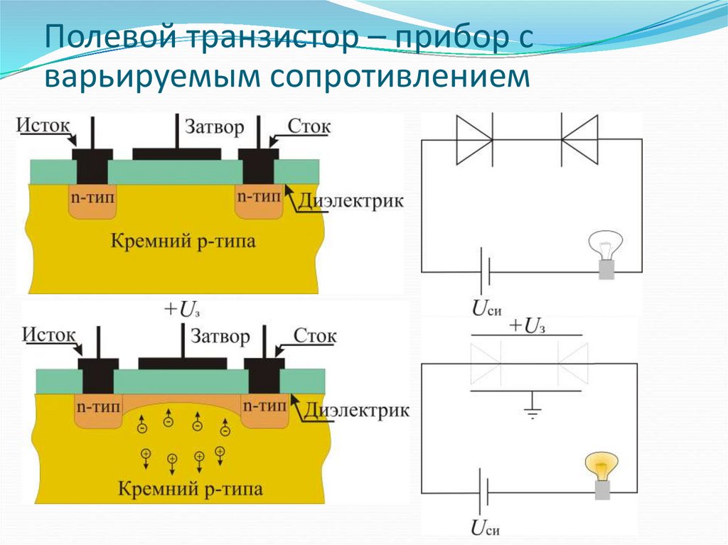
Полевой транзистор – прибор сварьируемым сопротивлением
4. The end of Moore’s ‘law’?
5.
IBM Gains Confidence in 22 nm ETSOI(IEDM Conf., Dec. 2009)
6. Intel Going Vertical for 22nm Transistors in 2011
7.
Multi-gate FETsN=2
N=3
N = 3,14
Intel Corp.
N = 3,4
N=4
N=3
8. Экспериментальный технологический маршрут изготовления МДП КНИ - нанотранзистора
Основные этапы изготовления :1. Формирование STI изоляции;
2. Изготовление затворного стека;
3. Изготовление спейсеров, истока/стока;
5. Изготовление контактов к стоку/ истоку;
6. Изоляция транзистора, формирование
контактных окон;
7. Металлизация.
9. Изготовление полевого транзистора
10. Изготовление полевого транзистора
11. Электронный литограф Raith-150
• 150x150mm stage for directwriting over 6” wafers
Automatic airlock for sample
loading
Schottky thermal fieldemission filament
200V-30kV beam acceleration
2pA-10nA beam current
2nm beam resolution at 20kV
Laser interferometer for stage
positioning with ~30nm
precision
12. Аналитический автоэмиссионный растровый электронный микроскоп для исследования наноструктур ULTRA ZEISS
1.0 нм при 15 кВ 1.7Пространственное
нм при 1 кВ
разрешение
4.0 нм при 0.1 кВ
12х – 900 000х в
режиме вторичных
электронов
100х – 900 000х в
режиме обратно
Диапазон увеличений рассеянных электронов
Автоэмиссионный
(термоэмиссионного
типа).Стабильность
Источник электронов лучше, чем 0.2% в час.
Диапазон ускоряющих
напряжений
20 В – 30 000 В
Диапазон рабочих
токов
4 пА – 20 нА
13. Установка атомно-слоевого осаждения FlexAl (Oxford Instruments Plasma Technology)
SubstratesUp to 200mm wafers
handling and pieces on
carrier plate
Precursosrs
Bubbled liquid and
solid precursors
Max precursor source
temperature
200ºC (oven and
jacket)
Additional precursors
Water + ozone
Mfc controlled gas lines
with rapid delivery system
1) thermal gas
precursors (e.g. NH3,
O2)
2) plasma gases (e.g.
O2, N2, H2)
In situ diagnostic features
Ellipsometry, OES
Swagelok 10ms rapid pulsing
ALD valves
Yes
Removable inner chamber
Yes
Wafer stage temperature
range
550ºC
14. Установки фотолитографии (Zuss) и нанесения резиста (Sawatec)
15. Установка плазмохимического травления Plasma Lab 100 Dual (Oxford Instruments Plasma Technology)
ICP Etch(380)Загрузка
шлюз
Подложки
до 200 мм
Диапазон температур
от -140°С до +400°С
Возбуждение плазмы
ВЧ
Линий газоподачи с РРГ
до 12 на каждую камеру
Плазменная очистка
камеры
есть
Вакуумная система
ТМН
Система управления
PC2000
Рабочие газы
HCl, C4H8, CF4, SF6, O2
16. Установка быстрого фотонного отжига Annealsys AS-100
Pyrometer and thermocouplecontrol
Fast digital PID temperature
controller
Temperature range: RT to
1200°C
Ramp rate up to 200°C/s
Cooling rate up to 100°C/s
RTA (Rapid Thermal
Annealing)
RTO (Rapid thermal
oxidation)
Diffusion, contact annealing
Nitridation
17. Теория наноэлектронных приборов
Требования современной электроники: Low-powerи High-performance
Альтернативные механизмы переноса тока:
туннелирование
Альтернативные материалы: графен и его
модификации
Масштабирование традиционных полевых
транзисторов;
18. SIMULATION
19. Эволюция моделей электронного транспорта
Charged waves:Schrödinger equation
Charged particles:
Boltzmann kinetic equation
Charged fluid:
Hydrodynamic equations
20. Квантовые эффекты в полевых нанотранзисторах
Поперечноеквантование;
Туннелирование и
интерференция
электронных волн;
Квантовая
статистика.
21. Silicon conduction band structure
Effective mass and transversalmt 0.19m0 , ml 0.98m0
quantization energy
0
2m d Si
2
2
22. Landauer-Büttiker formalism
GATES
O
U
R
C
E
1i
D
R
A
I
N
Tij
Rij
Transversal quantization
Landauer-Buttiker formalism
2e
(wave-guide modes) in a channel I (VD )
h
dET ( E ) f ( E ) f
ij
i
j
S
D
( E )
23. Everlasting controversy in kinetic simulation
Distribution function (equilibrium) is known only incontacts
Strong scattering in contacts
24. Heavy doping – low doping junction at S/D contact
Few of incident particlessurmount the barrier
=>
Equilibrium distribution
for particles
coming in the channel
-1
2.0x10
Potential energy, [eV]
0.0
-1
-2.0x10
-1
-4.0x10
-1
-6.0x10
-1
-8.0x10
Potential energy for different drain voltage
F ermi level in source contact
0
-1.0x10
-10
-5
0
5
10
x, [nm]
High self-consistent barrier at S/D contacts
Analytical solution obtained
for modified (BGK)
collision integral
in τ-approximation
25. Main strategy of simulation
Self-consistent solution ofSchrödinger equation
+
Maxwell equation
(Poisson equation)
26. Solution of 3D Schrödinger equation
22m
( x, y, z ) V ( x, y, z ) ( x, y , z ) ( x, y , z )
V(x,y,z) is a potential.
The direct solution of the stationary 3D Schrödinger
equation via a finite difference scheme comes across a
well known instability caused by evanescent modes.
In fact, the exponential growth of upper modes
makes a computation impossible.
27. D.K.Ferry et al. (2005) (США, Arizona State University): results of simulation
28.
Solution of Schrödinger equation:transverse mode representation + high-precision
arithmetic
( x, y , z )
N
a ( x )
i 1
i
i
( y, z )
where ψi(y,z) is the i-th transverse mode wave function,
N is a number of involved modes.
The space evolution of coefficients ai(x) is governed by matrix elements
M ij ( x ) i ( y, z ) | V ( x, y, z ) | j ( y, z )
The off-diagonal elements Mij manage the mode conversion.
The diagonal elements Mii manage the quantum reflection, interference and tunneling of the i-th mode.
29. Calculated transmission coefficient T(E) vs. electron energy E
(4 random impurities in a channel)1.2
1.2
1
Transmission
Transmission
1
0.8
0.6
0.4
0.8
0.6
0.4
0.2
0.2
0
0
0
0.1
0.2
0.3
0.4
Energy, eV
[100] and [010] valleys
0.5
0
0.1
0.2
0.3
0.4
Energy, eV
[001] valleys
Transistor parameters are 10nm channel length and width, 5nm body thickness,
10^20 cm^-3 source/drain contact doping, 5nm contact length.
0.5
30. Gate voltage characteristics
Drain Current, [A]1E-5
Vd=0.9
Vd=0.05
1E-6
1E-7
1E-8
-0.4
-0.2
0.0
0.2
0.4
0.6
Gate Voltage, [V]
Sub-threshold swing is 71 mV per decade of current.
0.8
1.0
31. Impurities in channel:
-5Drain Current, [A]
1.2x10
-6
8.0x10
without impurities in channel
1 positive impurity in channel
1 negative impurity in channel
channel thickness 3 nm
-6
4.0x10
0.0
0.0
0.2
0.4
0.6
Drain Voltage, [V]
0.8
1.0
32. Impurities in channel:
-5Drain Current, [A]
1.2x10
-6
8.0x10
without impurities in channel
1 impurity near drain
1 impurity near source
channel thickness 3 nm
-6
4.0x10
0.0
0.0
0.2
0.4
0.6
Drain Voltage, [V]
0.8
1.0
33. Corrugated channel:
-5Drain Current, [A]
1.2x10
-6
8.0x10
flat channel
corrugated channel ( 0.5 nm step)
channel thickness 3 nm
-6
4.0x10
0.0
0.0
0.2
0.4
0.6
Drain Voltage, [V]
0.8
1.0
34. Corrugated channel:
-5Drain Current, [A]
1.2x10
-6
8.0x10
without narrow in channel
Narrow Left 0.5 nm
Narrow R ight 0.5 nm
channel thickness 3 nm
-6
4.0x10
0.0
0.0
0.2
0.4
0.6
Drain Voltage, [V]
0.8
1.0
35. Dispersion of characteristics
5-15% in calculated I-V curves< 10% is an everlasting condition for large integrated
circuits
More severe demands to technology may arise.
36.
Требования к современнойэлектронике
37. Требования к современной электронике: 1) high performance
RC задержка инвертораdelay time = Rin * Cout
Предельная частота:
пролётное время
v
f max
Lch
Необходима высокая
проводимость канала
транзисторов и малый
размер транзистора
Необходима малая
длина канала
(Intel – 22nm)
и/или высокая
подвижность (новые
материалы)
38. Требования к современной электронике: 2) low power
ПотребляемаяПассивная мощность
активная мощность
2
CVDD
Pa
f
2
Необходимо малое
напряжение питания и
быстрое переключение
между состояниями
Pp I OFFVDD
Необходим малый ток
в закрытом состоянии
Большое отношение
I ON / I OFF
39. Снижение энергопотребления
Предельная крутизна переключения: 60 мВ/декдля термоэмиссионого механизма переноса тока
Как сделать круче?
40.
Туннельные транзисторыпозволяют достичь
подпороговой крутизны выше (60мВ/дек)-1
при комнатной температуре
41. Tunnel FET vs. thermionic FET
eVI exp B
kT
d ln I
e
1
60 mV/dec
dVG
kT
Limits the drive voltage VDD>240 mV
to achieve 4 decade switching
Fcr
I Ev Ec VG exp
F
V
G
d ln I
dVG
Ec Ev
Low voltage switching possible –
low power operation
42. Tunnel transisors
Shottky-barrier FETGate-controlled reverse-biased
Shottky junction
Intraband metalsemiconductor tunneling
Interband tunnel FET
Gate-controlled reverse-biased
Esaki junction
Valence-to-conduction band
tunneling
43. Shottky-barier TFETs: ultimate subthreshold slope
I I tun I thermb
I therm exp
kT
4 2m 3
b
I tun exp
3
e
F
V
G
The subthreshold slope of tunnel
component is large only when
tunnel component is small and
masked by thermionic current
The (60 mV/dec)-1 limit persists
for SB FET despite the presence
of tunneling
Schematic view of current components in SB
FET vs gate voltage illustrating the
impossibility to achieve subthermal steepness
D. Svintsov et.al. Semiconductors 47, p. 279 (2013)
W. G Vandenberghe. et al. Appl. Phys. Lett. 102,
013510 (2013)
44. TFETs subthreshold: state of the art
H. Lu ans A.C. Seabaugh IEEE Journal of the Electron Devices Society 2 p. 44-49 (2014)45. Limits of the subthreshold slope: band tails
Nonzero currentdue to tunneling
from the DOS
tails!
E.O. Kane Phys. Rev. 131, (1963)
S. Mookerjea et. al. IEEE EDL 31 (2010)
C.D. Bessire et. al. Nano Lett. 11 (2011)
46. Limits of the subthreshold slope: band tails
E.O. Kane 1963 Phys. Rev 131 p. 79Comparison of TFET modeling with
perfectly flat bands (dashed) and taking
into account the band tails (solid)
47. Multigate TFET with electrically induced p-n junction
48. Simulated characteristics of MG-TFET
Simulated characteristics of MGTFET•Gate dielectric 2 nm, κ=25
(e.g. HfO2);
•Distance between gates
(“doping” and “control”
gates) is 2 nm;
•10 nm SOI thickness;
•Better subthreshold due to
tunneling
in
undoped
region (no band tails);
•Higher current due to
abrupt
screening
of
potential
below
the
“doping” gate.
Simulated I(VG)-curve for multigate FET with
electrically induced junctions (MG TFET, solid) and
common FETs with doped source and drain
49.
Graphene FETs50. Graphene and nanotubes: electronic properties
Semiconductor NTGraphene electronic spectrum
Metallic NT
51. Graphene structures
Deposited or epitaxial (on SiC orhBN) graphene: mobility 500010000 cm^2/V s due to
interface defects and bulk phonons
Suspended graphene or twisted
graphene stack: mobility 100000200000 cm^2/V s
no
interface defects and bulk phonons
52. Электронные свойства графена
53. FET structure
54. Модель транспорта электронов в графене
Высокая частота межэлектронных столкновенийпозволяет описывать транспорт в гидродинамической
модели
2
ρe u e ε e
ue
φ
1 2 ene
βe i ue βeh ue uh ,
t
x 2
vF
xi
2
uh
εh
φ
1 2 enh
βh i uh βeh uh ue .
t
x 2
v
x
i
F
ne , nh electron and hole concentrations
ρh u h
ρe , ρh electron and hole mass densities ρ nm0
ue , uh drift velocities
βe i , βh i friction coefficients
n
n0
1 u / vF 2
,ρ
3/ 2
ρ0
1 u / vF 2
5/ 2
D. Svintsov, V. Vyurkov, S. Yurchenko, V. Ryzhii, T.
Otsuji "Hydrodynamic model for electron-hole
plasma in graphene", Journal of Applied Physics,
Vol. 111, p. 083715 (2012)
D. Svintsov, V. Vyurkov, V. Ryzhii, T. Otsuji
“Hydrodynamic electron transport and nonlinear
waves in graphene”, Physical Review B, Vol. 88, p.
245444 (2013)
55. Моделирование характеристик полевых транзисторов
ЭкспериментТеория
Теория
Эксперимент
Моделирование характеристик полевых
транзисторов
56. Bipolar graphene FET channel
Vd < VgVd > Vg
Vd = 2Vg
Vd > 2Vg
57. Possible applications: Logic circuits?
Graphene=> good Ohmic source
and drain contact
Gap=0
=> big OFF-state current
Bilayers, nanoribons or graphane
=> bad Ohmic source and
drain contact
Gap≠0
=> low OFF-state current
58. Graphene vertical tunnel FETs
Layout of vertical graphene tunnel FET.Tunneling occurs between two graphene layers
separated by 3-10 monolayers of boron nitride
Band diagram of graphene lateral TFET. The
gate voltage controls the tunnel density of
states, but not the barrier height
L. Britnell et al ,Science vol. 335 p. 947 (2012)
L. Britnell et. al., Nature Communications vol. 4 art. no. 1794 (2013)
59. Graphene vertical tunnel FETs
Measured tunnel conductivity of verticalgraphene TFET vs. gate voltage
L. Britnell et. al., Science 335 p. 947 (2012)
T. Georgiou et. al. Nature Nanotechnology 8 p. 100 (2013)
A. Mishchenko et. al. Nature Nanotechnology 9 p. 808 (2014)
Calculated current gain of vertical graphene
TFET vs. frequency at different electron Fermi
energies in source layer. Cutoff frequency
~10MHz expected due to small tunneling
probability
60. Латеральный туннельный транзистор на основе графена
Структуры предлагаемых транзисторовD. Svintsov et. al., Semiconductors vol. 47, p. 279-284 (2013)
D. Svintsov et. al., J. Phys. D: Appl. Phys. Special issue “Graphene devices” (2014)
Рассчитанные характеристики, демонстрирующие
насыщение тока и высокое (>104) отношение
токов открытого и закрытого состояний
61. Транзисторы на основе двухслойного графена
γ12 Δ2ε p
p 2 vF2
2
4
2
γ14
p 2 vF2 γ12 Δ2
4
D. Svintsov, V. Vyurkov, V. Ryzhii, T. Otsuji "Effect of "Mexican Hat"
on Graphene Bilayer Field-Effect Transistor Characteristics", Japanese
Journal of Applied Physics, Vol. 50, Iss. 7, p. 070112 (2011)
62. Graphene bilayer
•Gap opening up to ~0.4 eV by transverseelectric field;
•Symmetric
dispersion
Conduction and valence band electron dispersions
in graphene under applied transverse electric field
“Mexican-hat”
band
63. Graphene bilayer
•Gap opening up to ~0.4 eV by transverseelectric field;
•Symmetric
dispersion
Conduction and valence band electron dispersions
in graphene under applied transverse electric field
“Mexican-hat”
band
Density of states in gapped graphene bilayer
demonstrating a van Hove singularity
64. Exploiting the van Hove singularity in tunneling
(A) Layout of the proposed graphene bilayer TFET with electrically defined sourceand drain regions (B) Band diagram of graphene bilayer TFET for the optimal
biasing conditions: VB > 0, US < 0, UD > 0. At zero top gate bias, VG = 0, the TFET
is switched on, while at VG < 0 it is switched off.
Schematic dependence of direct interband tunneling current
on the band overlap in parabolic band semiconductors of
different dimensionality (3D, 2D, 1D) and graphene bilayer.
65. Graphene bilayer TFET characteristics
Calculated room-temperature gate transfer (left) and current-voltage (right) characteristics ofgraphene bilayer TFET at fixed bias voltages at auxiliary gates: VB = 3.3 V, US = −0.6 V, UD = 0.25 V. Top
gate dielectric is 2 nm ZrO2, κ = 25, back gate dielectric is 10 nm SiO2, spacing between the source
doping and control gates dg = 5 nm, spacing between drain doping and control gates is 10 nm. The regions
highlighted in yellow correspond to the drive voltage swing of 150 mV, in which sufficient ON/OFF ratio and
high ON-state current are achieved. Inset: gate transfer characteristic in the log scale.
66. Proposed FET positioning
67. Observation of interband tunneling in GBL
D. A. Bandurin, D. Svintsov, I.Gayduchenko, S. G. Xu, A. Principi, M.
Moskotin, I. Tretyakov, D. Yagodkin, S.
Zhukov, T. Taniguchi, K. Watanabe, I. V.
Grigorieva, M. Polini, G. Goltsman,A. K.
Geim, G. Fedorov “Resonant Terahertz
Detection Using Graphene Plasmons”
arXiv:1807.04703
68. QUANTUM COMPUTERS
69. History
Soviet mathematician Yu. Manin (1980) andR. Feynman (1982) proposed to use a quantum system (quantum
computer) for simulation of quantum systems.
Shor’s algorithm (1994): for integer factorization (to undermine the
modern secret communication):
N is a number of digits
N
Classical factoring algorithm ~
Shor’s quantum factoring algorithm ~ N 3
Grover’s algorithm (1996): search in unsorted data base of N elements
2
quantum ~
,
N
classical ~ N
70. Bit vs. Qubit
BitQubit
Discrete |0> or |1>
Analog |0> and |1>
Qubit superpositional state
| | 0 |1|
| |2 | |2 1
71. Classical register vs. Quantum register
BitsClassical register
|1>|0>|1>|1>|0>…
N bits of information
Qubits
Quantum register
2
N
Entangled states
-dimensional Hilbert space:
huge information capacity
2300
Sequential computation
> number of atoms in Universe
Quantum parallelism of computation
Great acceleration of several algorithms!
72. Entangled states in quantum computer: quantum parallelism
73. Realism and locality in quantum mechanics
74. EPR pair (EPR paradox => non-locality)
EPR pair (EPR paradox => non-locality)1
(| | | | )
2
EPR pair of photons is produced in non-linear crystal via down-
conversion.
One photon is in Alice disposal, the next one is in Bob’s disposal.
Wave function of Bob’s photon is collapsed after Alice’s measurement.
Is information instantly transmitted form Alice to Bob and the
relativity principle broken? No.
The name “Eve” originates from the word “eavesdropping” –
подслушивание.
75. Bomb paradox (Elitzur и Vaidman) => no realism
Bomb paradox (Elitzur и Vaidman)=> no realism
76. No cloning theorem
ProofThe linearity of time evolution operator U(Δt) implies
Consequences:
‘--’ quantum computing – error correction much
complicated
‘++‘ quantum communication – secrecy is possible
77. Quantum communication: Alice – Bob – Eve (eavesdropping)
I. EPR pairsAlice --------------- Bob
↑
EPR pair ↑
II. Single photons
Alice -- --------- Bob
78. Realizations of quantum computers
Dopant atoms in siliconQuantum dots
Ions in traps
Cold atoms in optic traps
NV-centers in diamond
Superconducting structures: charge, phase and
transmon
2D electron gas with Quantum Hall Effect
2D electron gas on Helium,
and so on
79. Classical vs. Quantum
BitsDiscrete |0> or |1>
Qubits
Analog Qubit superpositional
state |0> and |1>
| | 0 |1|
Accuracy 10-4
Noise (decoherence) and technological variability!!!
Error correction???
80. Classical vs. quantum
81.
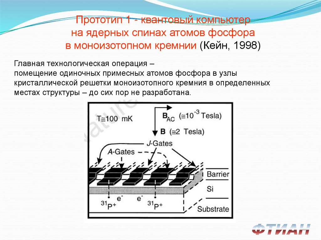
Прототип 1 - квантовый компьютерна ядерных спинах атомов фосфора
в моноизотопном кремнии (Кейн, 1998)
Главная технологическая операция –
помещение одиночных примесных атомов фосфора в узлы
кристаллической решетки моноизотопного кремния в определенных
местах структуры – до сих пор не разработана.
82. Предыстория
Квантовый компьютер на основе двойных квантовых точках. Fedichkin, M. Yanchenko, K.A. Valiev, Nanotechnology 11, 387 (2000) 141, 146 39.
Квантовый компьютер без перемещения заряда (борьба с
декогерентизацией)
V. Vyurkov, S. Filippov, L. Gorelik. Quantum computing based on space states
without charge transfer. Physics Letters A 374, 3285–3291 (2010)
Измерение состояния квантового регистра в канале
транзистора в режиме кулоновской блокады тока
M. Rudenko, V. Vyurkov, S. Filippov, A. Orlikovsky. Quantum register in a field-
effect transistor channel. Int. Conf. “Micro- and nanoelectronics – 2014”, Moscow,
Russia, October 6-10, 2014, Book of Abstracts, p. q1-05
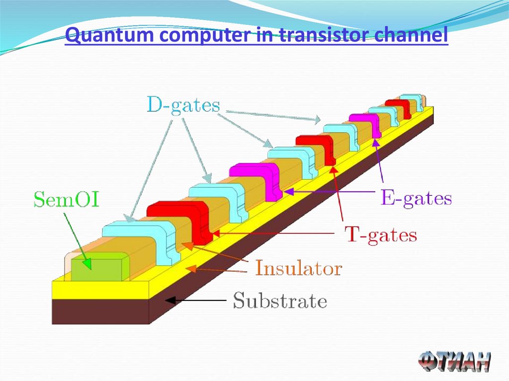
83. From quantum transistor to quantum computer
Quantum confinement;Tunneling and
interference of electron
waves;
Quantum statistics.
84.
Quantum computer in transistor channel85. 1а. Технический облик - лабораторный
1а. Технический облик лабораторныйМикросхема регистра с контактами
Измерительная установка
86. 1б. Технический облик - коммерческий
1б. Технический облик коммерческийИнтегральная схема регистра с управляющей и измерительной
системой
87. Field-defined quantum dots
Symmetric state in DQDAsymmetric state in DQD
88. Basic states in a DQD
Electron wave-function in a DQDSymmetric
Antisymmetric
Potential in a DQD
89. Basic states of two DQDs (without charge transfer !)
basis*Potential in two DQDs
Wave-function of two
electrons in two DQDs
90. Basic states of a qubit
Spin-polarized electrons:1
0
1 2 2 1
2
1
1
1 2 2 1
2
91. Qubit states
10
1 2 2 1
2
r1
r2
r1
r2
92. Qubit states
11
1 2 2 1
2
r1
r2
r1
r2
93. Realization of SWAP-gate
94. Realization of sqrt-SWAP
95. Realization of CNOT-gate
96. Coulomb blockade of current for measurement
Dot occupied => potential barrierDot vacant => potential well
Rough condition of Coulomb blockade: dot size D > Bohr radius
97. Calculated transmission coefficients
For fairly smooth potential profile the transmission through the well tends to 1whereas the transmission through the barrier tends to 0
98. Альтернативные проекты QC во ФТИАН
99. Квантовый регистр на основе двойных квантовых точек в оптическом резонаторе
100.
Квантовые компьютеры на NV-центрах в алмазеИскусственные алмазы:
теплопроводность
> 2000 Вт/м К
скорость звука
с = 17300 м/с
плотность
= 3515 кг/м3
модуль Юнга
E ~ 1000 ГПа
Спиновый кубит на
электронных уровнях
NV-центра
S z 1 1
3A
2
S z 1 0
101. Эпилог
СLight at the end of the tunnel
102. Collaboration
АО Микрон и НИИМЭНаноэлектронные технологии
ИФП СО РАН
Фраунгоферовский институт (Германия)
Графен
Лаборатория двумерных систем МФТИ (Д. Свинцов)
Университет Тохоку (Япония)
ИПТМ РАН
ТГц
МГУ им. М.В. Ломоносова
ИСВЧПЭ РАН
Квантовые компьютеры
Лаборатория квантовой информатики МФТИ (С. Филиппов)
МГУ им. М.В. Ломоносова
ИФП СО РАН
103.
104.
105.
106.
107.
108. Квантовые эффекты в полевых нанотранзисторах
•Уравнение Шредингера:•Уравнение Пуассона:
•Формула Ландауэра:
2
2m
( x, y, z ) V ( x, y, z ) ( x, y, z ) ( x, y, z)
4
en
2e
I
h i 0
dET ( E ) f ( E ) f
i
s
d
( E )
109. Теория наноэлектронных приборов
Цели современной наноэлектроники: Low-power иHigh-performance
Альтернативные механизмы переноса тока:
туннелирование
Альтернативные материалы: графен и его
модификации (в сотрудничестве с университетом
Тохоку, Япония)
Масштабирование традиционных полевых
транзисторов.
110. Транзисторы на основе графена: новые вопросы
Объяснение отрицательной дифференциальной проводимости;Амбиполярные эффекты в полевых транзисторах – одновременное
наличие электронов и дырок;
Создание инжекционных лазеров на основе графена.
V. Ryzhii, I. Semenikhin, M. Ryzhii, D. Svintsov, V. Vyurkov, A. Satou, and T. Otsuji “Double
injection in graphene p-i-n structures”, Journal of Applied Physics, Vol. 113, p. 244505 (2013)
111. Basic states in a DQD
Electron wave-function in a DQDSymmetric
Antisymmetric
Potential in a DQD
112. Coulomb blockade for measurement
113. Терагерцовые лазеры на основе графена
114. Терагерцовые лазеры на основе графена
Создание квантовой теории оптического поглощения в графенес неравновесными носителями;
Расчет рекомбинационных процессов, обусловленных
взаимодействием квазичастиц.
115. Электронные свойства графена
Бесщелевойполупроводник;
Линейный закон
дисперсии
0
ˆ
H vF
pˆ x ipˆ y
pˆ x ipˆ y
0
ε p = p vF
Отсутствие обратного
рассеяния
p | V r r | p
1 cos θ
2
Vq
pp