
Similar presentations:

 Optical")
 An introduction")


Creation of light-emitting structures based on CdSe nanoplatelets
1.
Creation of light-emitting structuresbased on CdSe nanoplatelets
Ruslan Azizov
PhD student 1st year
Scientific supervisor: Sergey Makarov
Faculty of Physics
2.
Introduction2
International Students and Scholars Rock k
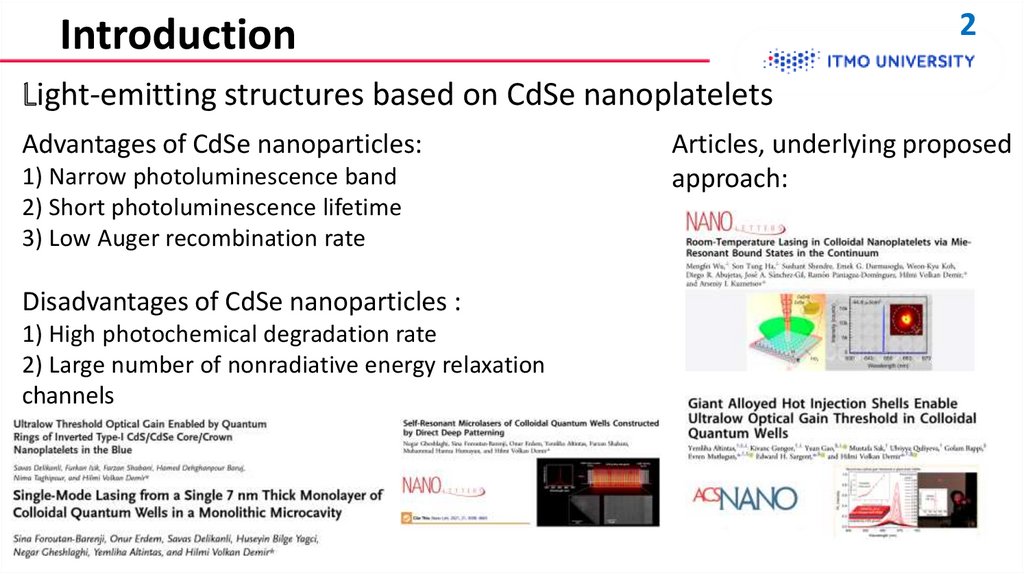
Light-emitting structures based on CdSe nanoplatelets
Advantages of CdSe nanoparticles:
1) Narrow photoluminescence band
2) Short photoluminescence lifetime
3) Low Auger recombination rate
Disadvantages of CdSe nanoparticles :
1) High photochemical degradation rate
2) Large number of nonradiative energy relaxation
channels
Articles, underlying proposed
approach:
3.
Purpose of research3
International Students and Scholars Rock k
Development and experimental investigation of resonant nanostructures
based on CdSe nanoplatelets for low-threshold laser generation
(full research cycle including numerical modelling, fabrication and postprocessing of CdSe NPL films, and measurement of emission characteristics)
4.
PLAN for 2021-20254
International Students and Scholars Rock k
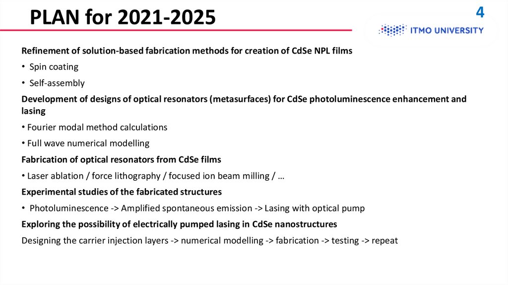
Refinement of solution-based fabrication methods for creation of CdSe NPL films
• Spin coating
• Self-assembly
Development of designs of optical resonators (metasurfaces) for CdSe photoluminescence enhancement and
lasing
• Fourier modal method calculations
• Full wave numerical modelling
Fabrication of optical resonators from CdSe films
• Laser ablation / force lithography / focused ion beam milling / …
Experimental studies of the fabricated structures
• Photoluminescence -> Amplified spontaneous emission -> Lasing with optical pump
Exploring the possibility of electrically pumped lasing in CdSe nanostructures
Designing the carrier injection layers -> numerical modelling -> fabrication -> testing -> repeat
5.
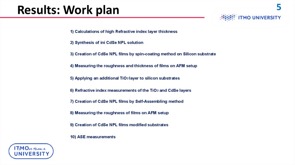
Results: Work plan1) Calculations of high Refractive index layer thickness
2) Synthesis of ini CdSe NPL solution
3) Creation of CdSe NPL films by spin-coating method on Silicon substrate
4) Measuring the roughness and thickness of films on AFM setup
5) Applying an additional TiO2 layer to silicon substrates
6) Refractive index measurements of the TiO2 and CdSe layers
7) Creation of CdSe NPL films by Self-Assembling method
8) Measuring the roughness of films on AFM setup
9) Creation of CdSe NPL films modified substrates
10) ASE measurements
5k
6.
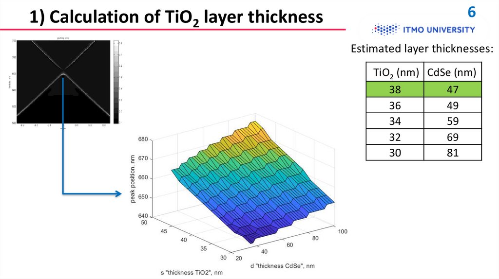
International Students and Scholars Rock6k1) Calculation of TiO2 layer thickness
Estimated layer thicknesses:
TiO2 (nm) CdSe (nm)
38
47
36
49
34
59
32
69
30
81
7.
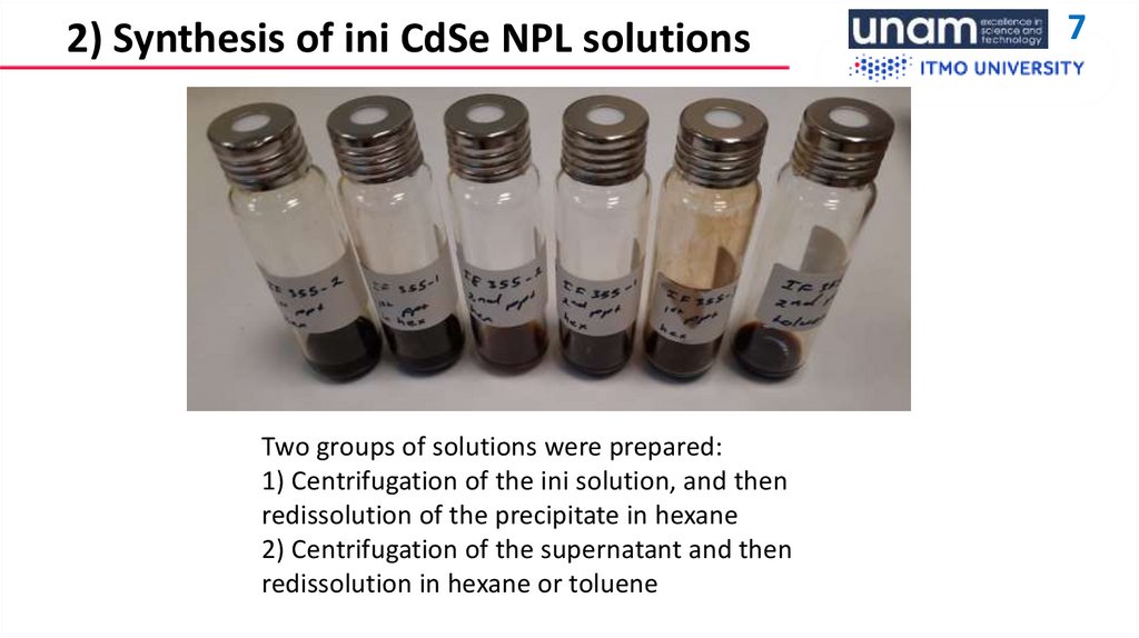
International Students and Scholars Rock7k2) Synthesis of ini CdSe NPL solutions
Two groups of solutions were prepared:
1) Centrifugation of the ini solution, and then
redissolution of the precipitate in hexane
2) Centrifugation of the supernatant and then
redissolution in hexane or toluene
8.
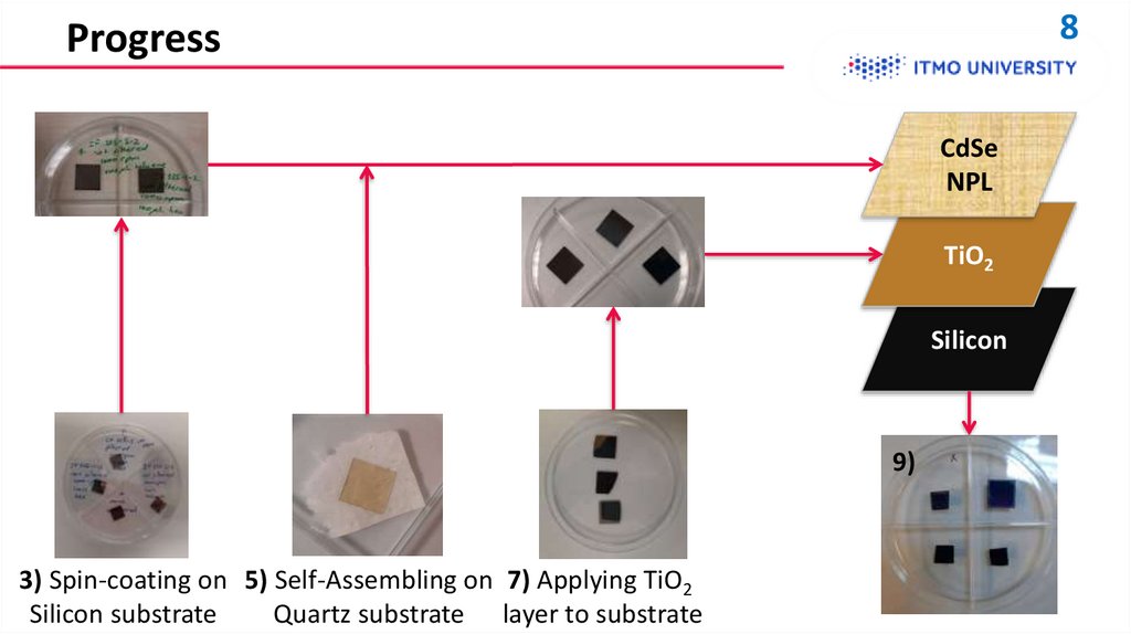
Progress8
International Students and Scholars Rock k
CdSe
NPL
TiO2
Silicon
9)
3) Spin-coating on 5) Self-Assembling on 7) Applying TiO2
Silicon substrate
Quartz substrate layer to substrate
9.
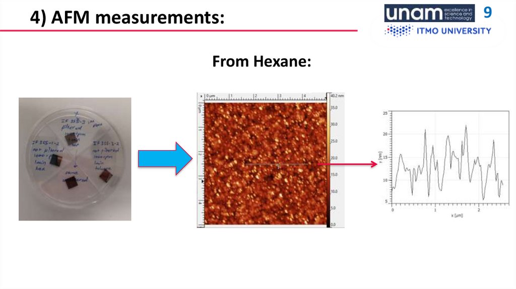
4) AFM measurements:From Hexane:
9
UNAM
International Students and
Scholars Rock k
10.
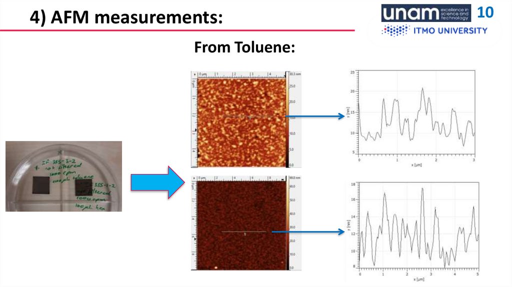
4) AFM measurements:From Toluene:
10k
UNAM
International Students and
Scholars Rock
11.
11kInternational Students and Scholars Rock
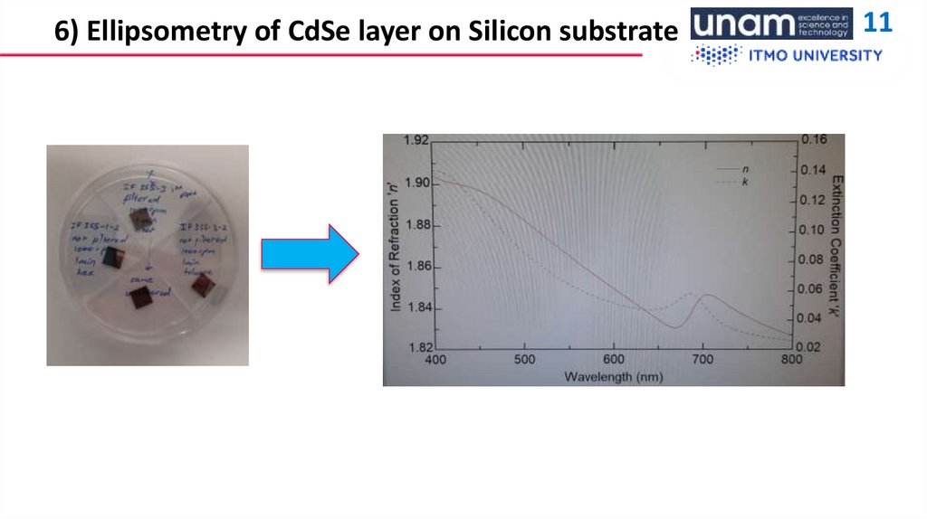
6) Ellipsometry of CdSe layer on Silicon substrate
12.
12kScholars Rock
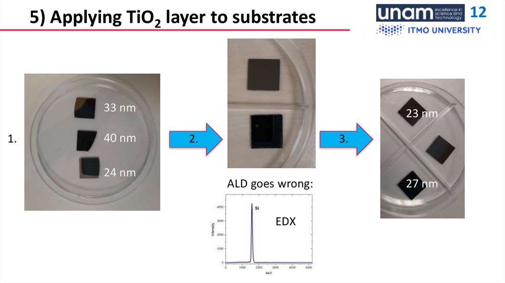
5) Applying TiO2 layer to substratesInternational Students andUNAM
33 nm
1.
40 nm
24 nm
23 nm
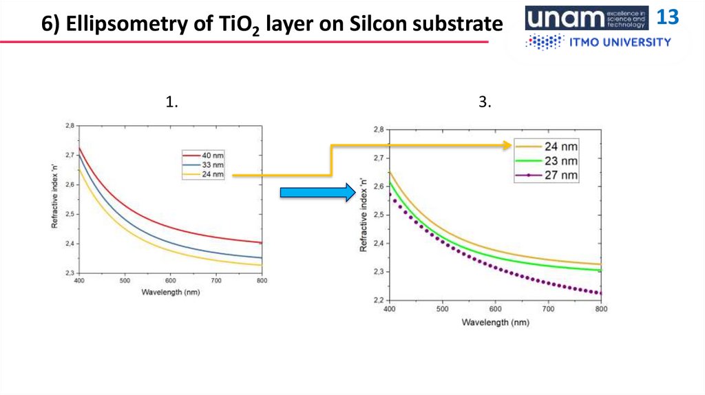
2.
3.
ALD goes wrong:
EDX
27 nm
13.
13kInternational Students and Scholars Rock
6) Ellipsometry of TiO2 layer on Silcon substrate
1.
3.
14.
14kUNAM
International Students and
Scholars Rock
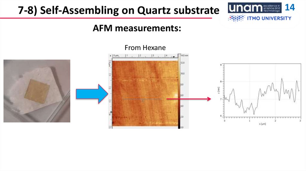
7-8) Self-Assembling on Quartz substrate
AFM measurements:
From Hexane
15.
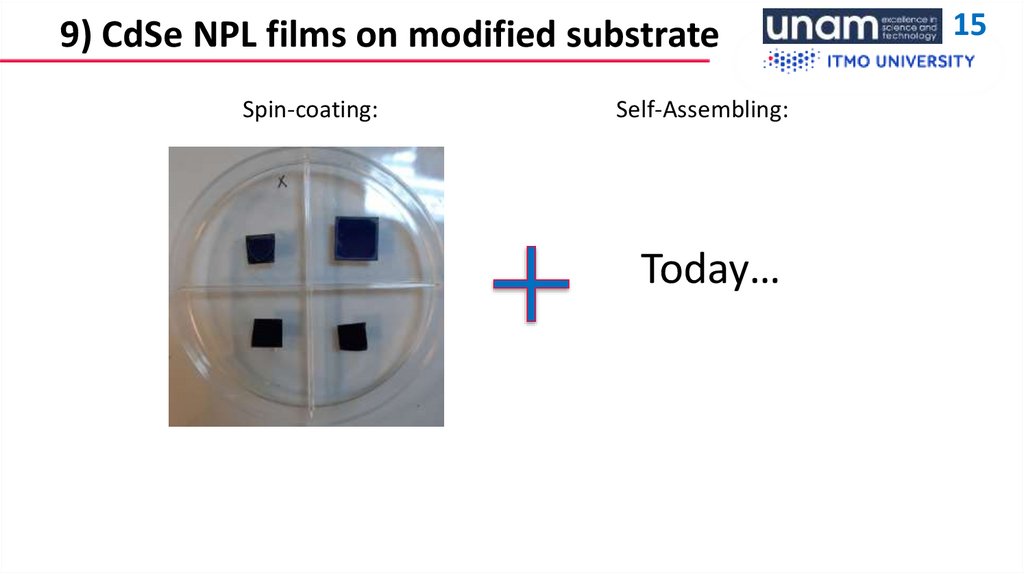
9) CdSe NPL films on modified substrateSpin-coating:
Self-Assembling:
Today…
15k