


")


")


")


 english
Similar presentations:


Basics Material Characterization Techniques. Structural (bulk and surface) Optical
1. Basics Material Characterization Techniques
Structural (bulk and surface)Optical
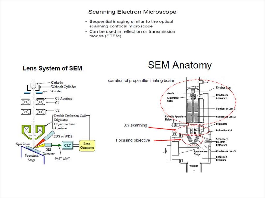
2. Basic Electron Microscopy
3.
4. Electron Microscopy - definition and types
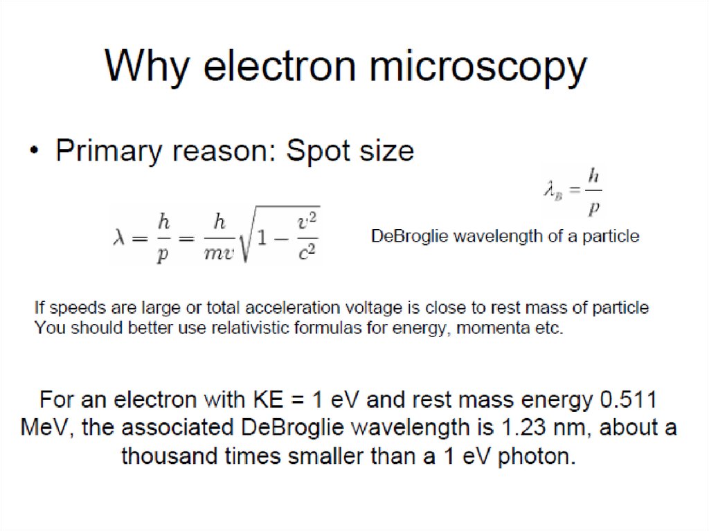
• Developed in the 1930s that use electron beamsinstead of light.
• because of the much lower wavelength of the
electron beam than of light, resolution is far
higher.
TYPES
• Transmission electron microscopy (TEM) is
principally quite similar to the compound light
microscope, by sending an electron beam through
a very thin slice of the specimen. The resolution
limit is less than 0.03 nanometer.
• Scanning electron microscopy (SEM) visualizes
details on the surfaces of cells and particles and
gives a very nice 3D view. The magnification is in
the lower range than that of the transmission
electron microscope.
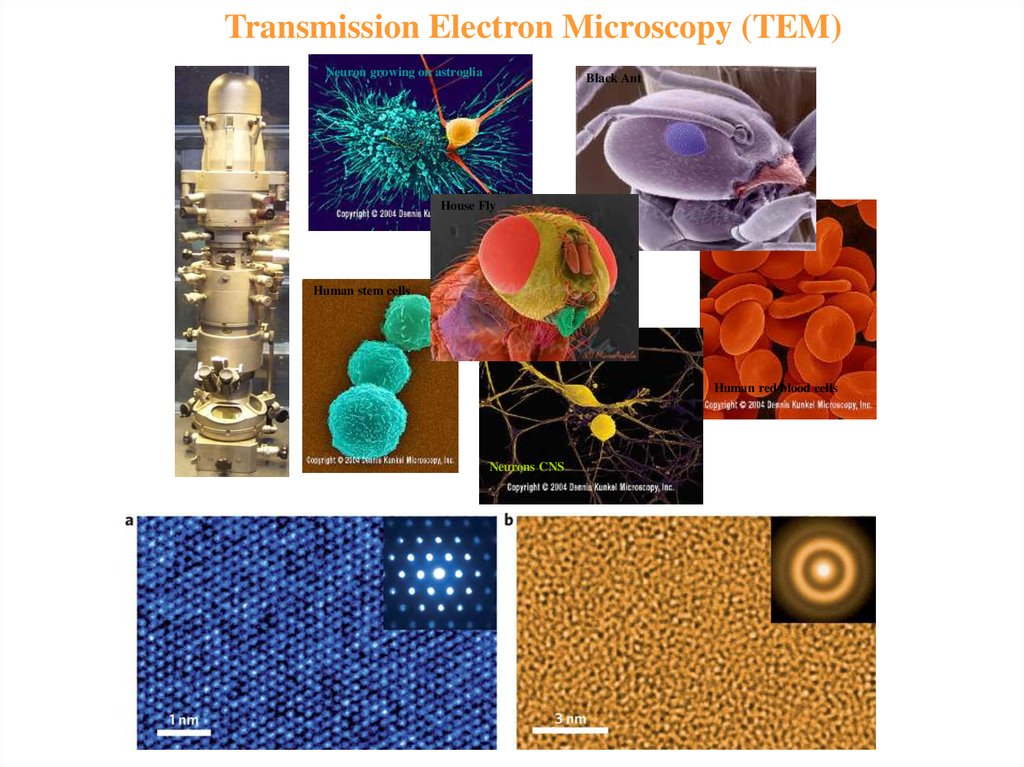
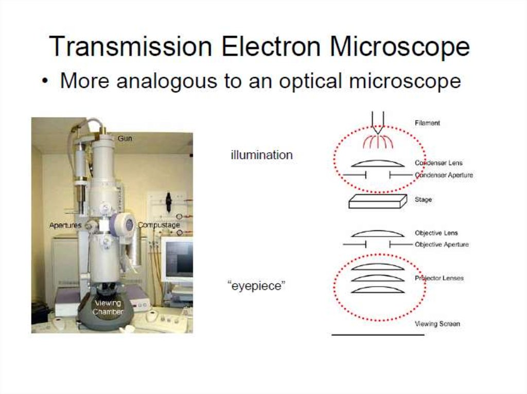
5. Transmission Electron Microscopy (TEM)
• beam of electrons is transmitted through a specimen, then animage is formed, magnified and directed to appear either on a
fluorescent screen or layer of photographic film or to be
detected by a sensor (e.g. charge-coupled device, CCD camera.
• involves a high voltage electron beam emitted by a cathode,
usually a tungsten filament and focused by electrostatic and
electromagnetic lenses.
• electron beam that has been transmitted through a specimen
that is in part transparent to electrons carries information about
the inner structure of the specimen in the electron beam that
reaches the imaging system of the microscope.
• spatial variation in this information (the "image") is then
magnified by a series of electromagnetic lenses until it is
recorded by hitting a fluorescent screen, photographic plate, or
CCD camera. The image detected by the CCD may be displayed
in real time on a monitor or computer.
6.
Transmission Electron Microscopy (TEM)Neuron growing on astroglia
Black Ant
House Fly
House Fly
Human stem cells
Human red blood cells
Neurons CNS
7.
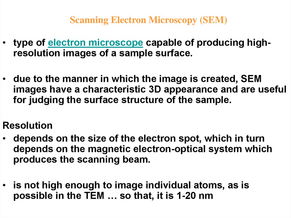
Scanning Electron Microscopy (SEM)• type of electron microscope capable of producing highresolution images of a sample surface.
• due to the manner in which the image is created, SEM
images have a characteristic 3D appearance and are useful
for judging the surface structure of the sample.
Resolution
• depends on the size of the electron spot, which in turn
depends on the magnetic electron-optical system which
produces the scanning beam.
• is not high enough to image individual atoms, as is
possible in the TEM … so that, it is 1-20 nm
8. the electron gun
9.
10.
11.
12.
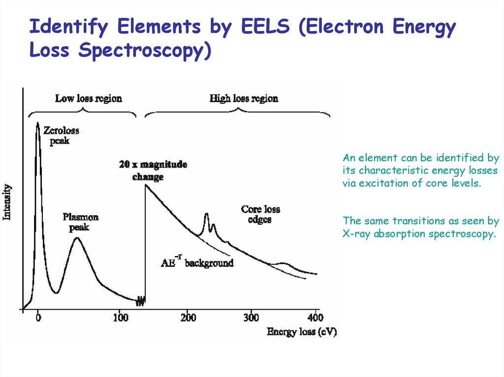
Identify Elements by EELS (Electron EnergyLoss Spectroscopy)
An element can be identified by
its characteristic energy losses
via excitation of core levels.
The same transitions as seen by
X-ray absorption spectroscopy.
13.
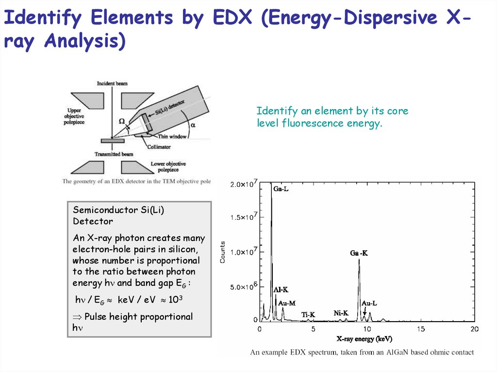
Identify Elements by EDX (Energy-Dispersive Xray Analysis)Identify an element by its core
level fluorescence energy.
Semiconductor Si(Li)
Detector
An X-ray photon creates many
electron-hole pairs in silicon,
whose number is proportional
to the ratio between photon
energy h and band gap EG :
h / EG keV / eV 103
Pulse height proportional
h
14.
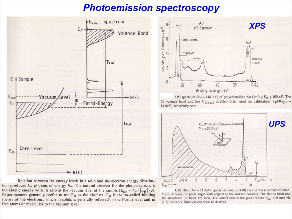
15. XPS spectoscopy
e0F
Vacuum Level
Fermi Level
Energy (eV)
• Photon removes a bound
electron according to:
KE = h - BE - F
• KE is the energy of the ejected
electron
• BE is the energy of the core
level
• Typical x-rays come from
thermionic emission of Al,
Mg, Cu, etc.
VB’s
h
L3
L2
L1
K
N (e)
16. Work Function
vac• Consequence of the
photoelectric effect
єF
Φ
e-
+
-
• Φ = EVAC - єF
єF
Φ
e-
+
• Adsorbates can increase
or decrease Φ
vac
-
• Important indicator of
physical and chemical
changes
17.
Photoemission spectroscopyXPS
UPS
18.
19. Scanning Tunneling Microscope (STM)
xyz-Piezo-Scannerz
high voltage
amplifier
y
x
probing tip
I
feedback
regulator
sample
Negative feedback keeps the current constant (pA-nA) by moving the tip up and down.
Contours of constant current are recorded which correspond to constant charge density.
20. Technology Required for a STM
• Sharp, clean tip(Etching, ion bombardment, field desorption by pulsing)
• Piezo-electric scanner
(Tube scanner, xyz scanner)
• Coarse approach
(Micrometer screws, stick-slip motors)
• Vibrational damping
(Spring suspension with eddy current damping, viton stack)
• Feed-back electronics
(Amplify the current difference, negative feedback to the z-piezo)
21.
Atomic resolution, several orders of magnitudebetter than the best electron microscope
Quantum mechanical tunnel-effect of electron
In-situ: capable of localized, non-destructive
measurements or modifications
material science, physics, semiconductor science,
metallurgy, electrochemistry, and molecular
biology
Scanning Probe Microscopes (SPM): designed
based on the scanning technology of STM
22. Theory and Principle
Tunneling CurrentA sharp conductive tip is brought to within a few
Angstroms of the surface of a conductor (sample).
The surface is applied a bias voltage, Fermi levels shift
The wave functions of the electrons in the tip overlap those
of the sample surface
Electrons tunnel from one surface to the other of lower
potential.
23.
24. Theory and Principle
In classical physics e flows are not possible without a directconnection by a wire between two surfaces
On an atomic scale a quantum mechanical particle behaves
in its wave function.
There is a finite probability that an electron will “jump” from
one surface to the other of lower potential.
25. Atomic Force Microscope (AFM)
deflectionsensor
cantilever
probing tip
feedback
regulator
sample
xy-piezo (lateral position)
high voltage
amplifier
z-piezo
(tip-sample distance)
Negative feedback keeps the force constant by adjusting the z-piezo such
that the up-down bending angle of the thin cantilever remains constant.
26. Deflection sensors
Photodiode withfour quadrants
Laser
27. Beam-deflection method
A light beam is reflected fromthe cantilever onto a photodiode
divided into 4 segments.
The vertical difference signal
provides the perpendicular
deflection.
The horizontal difference signal
provides the torsional bending of
the cantilever.
The two deflections determine
perpendicular and lateral forces
simultaneously.
28. AFM Cantilever and Tip To obtain an extra sharp AFM tip one can attach a carbon nanotube to a regular, micromachined silicon
tip.40 m
29.
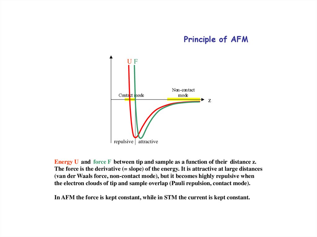
Principle of AFMV(r)
UF
Contact mode
Non-contact
mode
rz
repulsive attractive
Figur e 3.16. Potential energy be tween tip and
sample as a func tion o f the distanc e between them.
po tential tip
i s attractive
when they
apart
Energy U and force FThe
between
and sample
asarea far
function
of their distance z.
(non-con tact), but it will become strong ly
The force is the derivative
(= slope)
ofarethe
energy.
is attractive at large distances
repulsive
when they
close
toge therIt
(contact).
(van der Waals force, non-contact mode), but it becomes highly repulsive when
the electron clouds of tip and sample overlap (Pauli repulsion, contact mode).
In AFM the force is kept constant, while in STM the current is kept constant.
30. Dynamic Force Detection
f(b)
(I)
(II)
amplitude
(a)
frequency
A
f0
frequency
The cantilever oscillates like a tuning fork at resonance. Frequency shift and amplitude change
are measured for detecting the force.
(a) High Q-factor = low damping (in vacuum):
Sharp resonance, detect frequency change, non-contact mode
(b) Low Q-factor = high damping (in air, liquid):
Amplitude response, detect amplitude change, tapping mode
31. STM versus AFM
STM is particularly useful for probingelectrons at surfaces, for example the
electron waves in quantum corrals or the
energy levels of the electrons in dangling
bonds and surface molecules.
AFM is needed for insulating samples.
Since most polymers and biomolecules
are insulating, the probe of choice for
soft matter is often AFM. This image
shows DNA on mica, an insulator.
32.
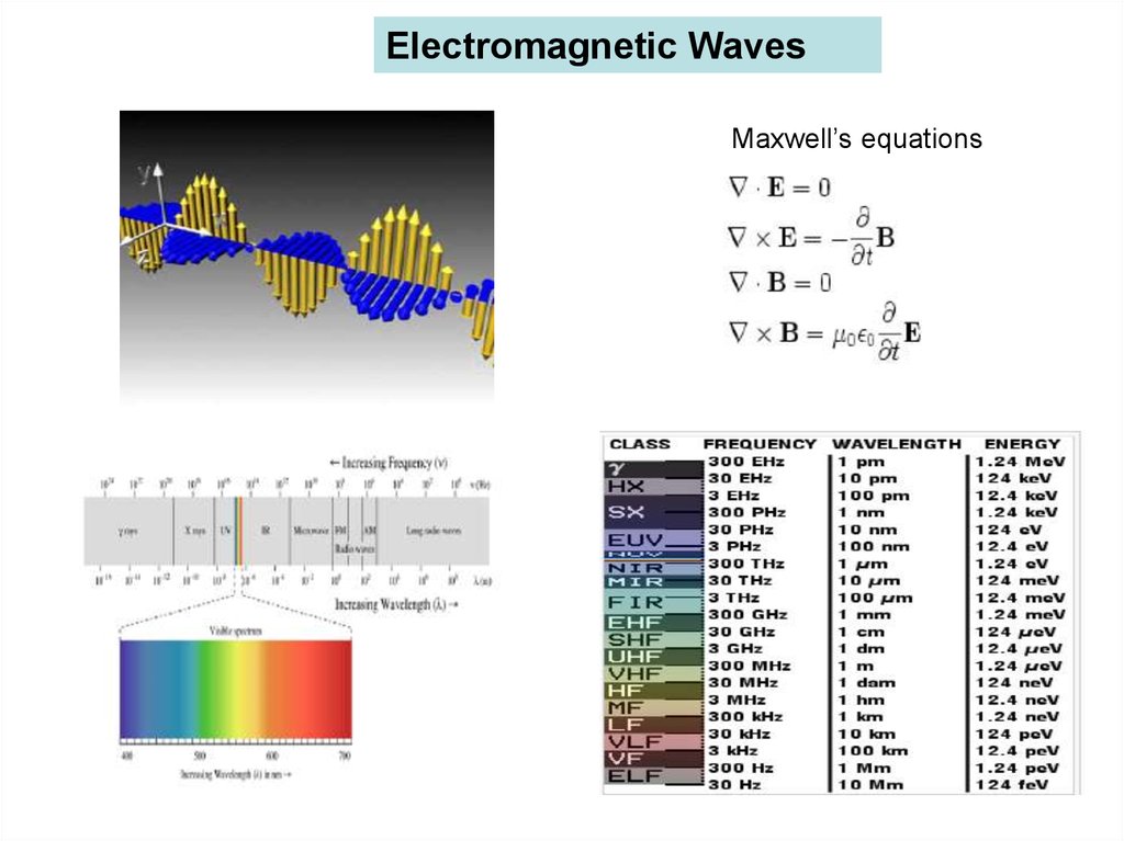
Electromagnetic WavesMaxwell’s equations
33.
34.
35. Energy Units for EM waves
• The Energy of EM waves is measured in severaldifferent units in the literature.
• E = h = hc/l
• 1 eV = 8065.5 cm-1 = 2.418 X 10¹⁴ Hz = 11,600 K.
• 1 eV = 1.2398 m
• 1 cm-1 = 0.12398 meV = 3X10¹⁰ Hz.
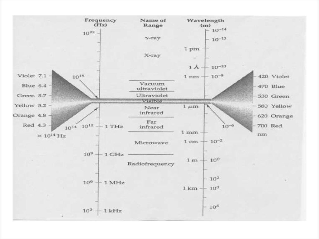
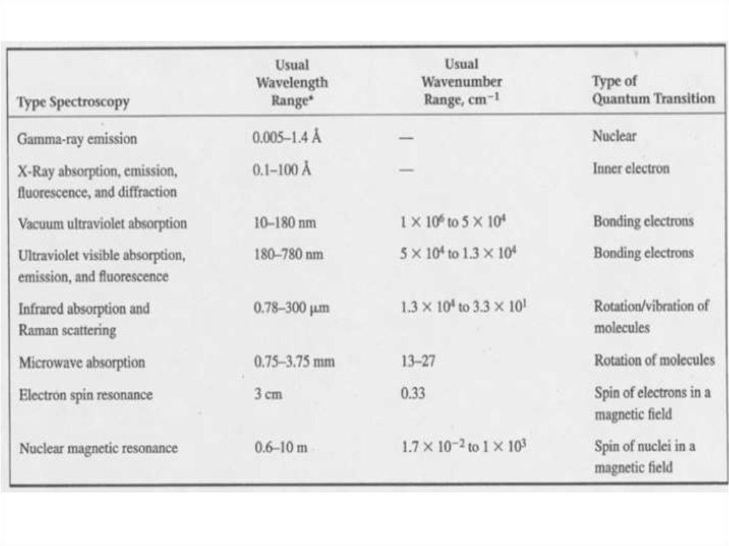
36.
UV-VIS spectroscopyCompound
l(nm)
Intensity/e
transition
with lowest
energy
CH4
122
intense
s-s* (C-H)
CH3CH3
130
intense
s-s* (C-C)
CH3OH
183
200
n-s* (C-O)
CH3SH
235
180
n-s* (C-S)
CH3NH2
210
800
n-s* (C-N)
CH3Cl
173
200
n-s* (C-Cl)
CH3I
258
380
n-s* (C-I)
CH2=CH2
165
16000
p-p* (C=C)
CH3COCH3
187
950
p-p* (C=O)
273
14
n-p* (C=O)
CH3CSCH3
460
weak
n-p* (C=S)
CH3N=NCH3
347
15
n-p* (N=N)
37. Linear spectroscopy Absorption Coefficient
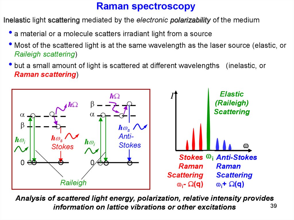
1. Free carrier absorption38. Raman Spectroscopy Basics
• Basic Physical Realization– Illuminate a specimen with laser light (e.g.
532nm)
– Scattered (no absorbed) Light in two forms
• Elastic (Rayleigh) → lscattered = lincident
• Inelastic (Raman) → lscattered lincident
– Light Experiences a “Raman Shift” in Wavelength
38
39.
Raman spectroscopyInelastic light scattering mediated by the electronic polarizability of the medium
• a material or a molecule scatters irradiant light from a source
• Most of the scattered light is at the same wavelength as the laser source (elastic, or
Raileigh scattering)
• but a small amount of light is scattered at different wavelengths
(inelastic, or
Raman scattering)
b
a
ћ
a
b
ћ i
ћ s
Stokes
ћ i
0
0
Raileigh
ћ
I
ћ s
AntiStokes
Elastic
(Raileigh)
Scattering
Stokes
Raman
Scattering
i- (q)
i Anti-Stokes
Raman
Scattering
i+ (q)
Analysis of scattered light energy, polarization, relative intensity provides
39
information on lattice vibrations or other excitations
40.
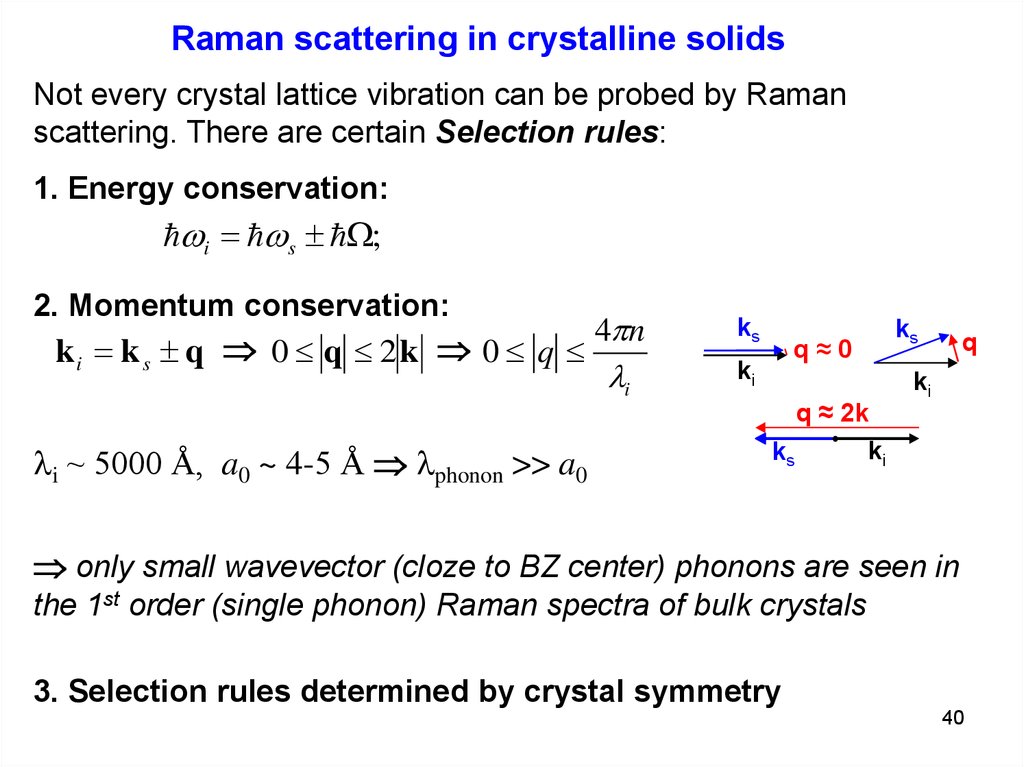
Raman scattering in crystalline solidsNot every crystal lattice vibration can be probed by Raman
scattering. There are certain Selection rules:
1. Energy conservation:
i s ;
2. Momentum conservation:
4pn
ki k s q 0 q 2 k 0 q
li
li ~ 5000 Å, a0 ~ 4-5 Å lphonon >> a0
ks
q≈0
ki
q ≈ 2k
ki
ks
ks
q
ki
only small wavevector (cloze to BZ center) phonons are seen in
the 1st order (single phonon) Raman spectra of bulk crystals
3. Selection rules determined by crystal symmetry
40
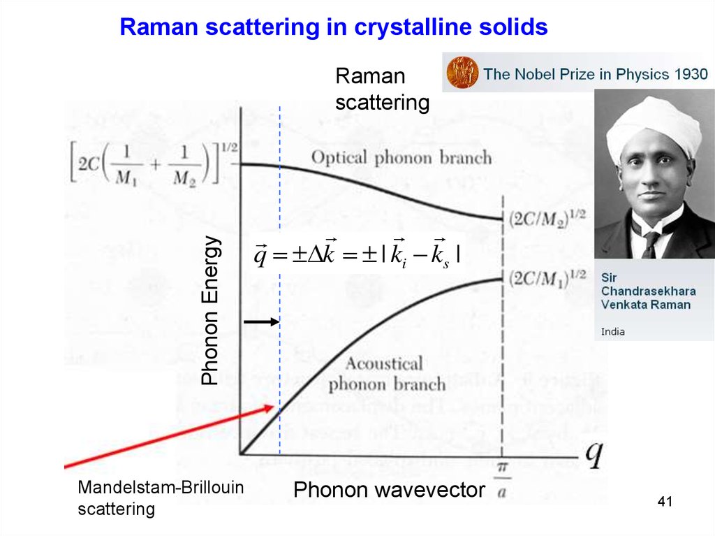
41.
Raman scattering in crystalline solidsPhonon Energy
Raman
scattering
Mandelstam-Brillouin
scattering
q k | ki - ks |
Phonon wavevector
41
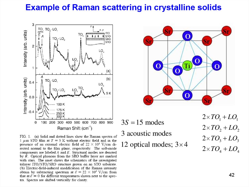
42.
Example of Raman scattering in crystalline solids3S 15 modes
3 acoustic modes
12 optical modes; 3 4
2 TO1 LO1
2 TO2 LO2
2 TO3 LO3
2 TO4 LO4
42
43.
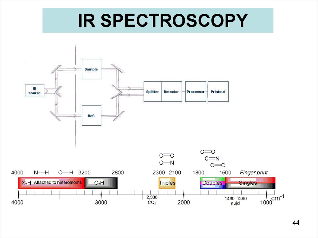
IR SPECTROSCOPYfar- infrared: 400-10 cm-1 (1000–30 μm), adjacent to the microwave region =>
rotational-vibrational
mid- IR: 4000-400 cm-1 (30–1.4 μm) => fundamental vibrations & rotational-vibrational
Near IR: 14000-4000 cm-1 (1.4–0.8 μm) can excite overtone or harmonic vibrations
Molecular Energy
E = Eel + Evib + Erot + …
Symmetrical
stretching
Antisymmetrical
stretching
Scissoring
Rocking
Wagging
Twisting
43
44.
IR SPECTROSCOPY44
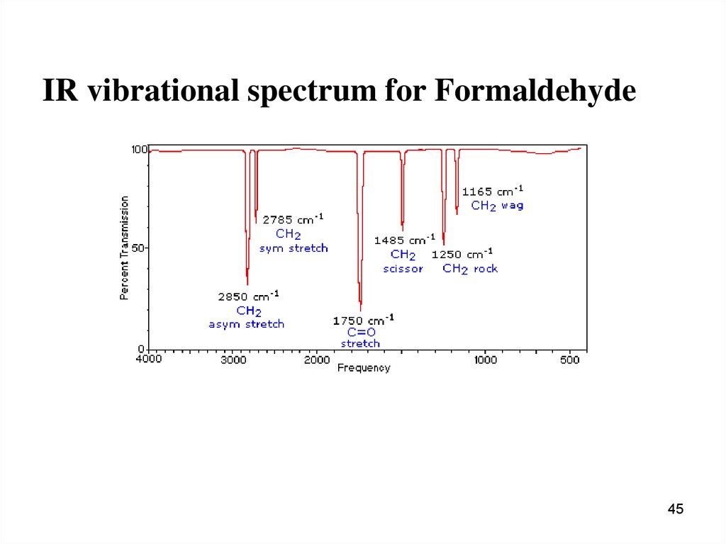
45.
IR vibrational spectrum for Formaldehyde45
46. Raman vs. FTIR
• FTIR– Sensitive to functional
group vibrations
especially OH stretch in
water, good for studying
the substituents on
organic molecules
– Usually needs some
sample prep for
transmission
– Good sensitivity
– Good
microscopic
technique
• Raman
– Sensitive to C=C, C≡C
• Distinguish diamondC from amorphous-C
• Studying backbone
vibrations of the
organic chain
– Little sample prep
– Fluorescence Light Can
Swamp Raman Light
– Fair sensitivity
– Good microscopic
technique
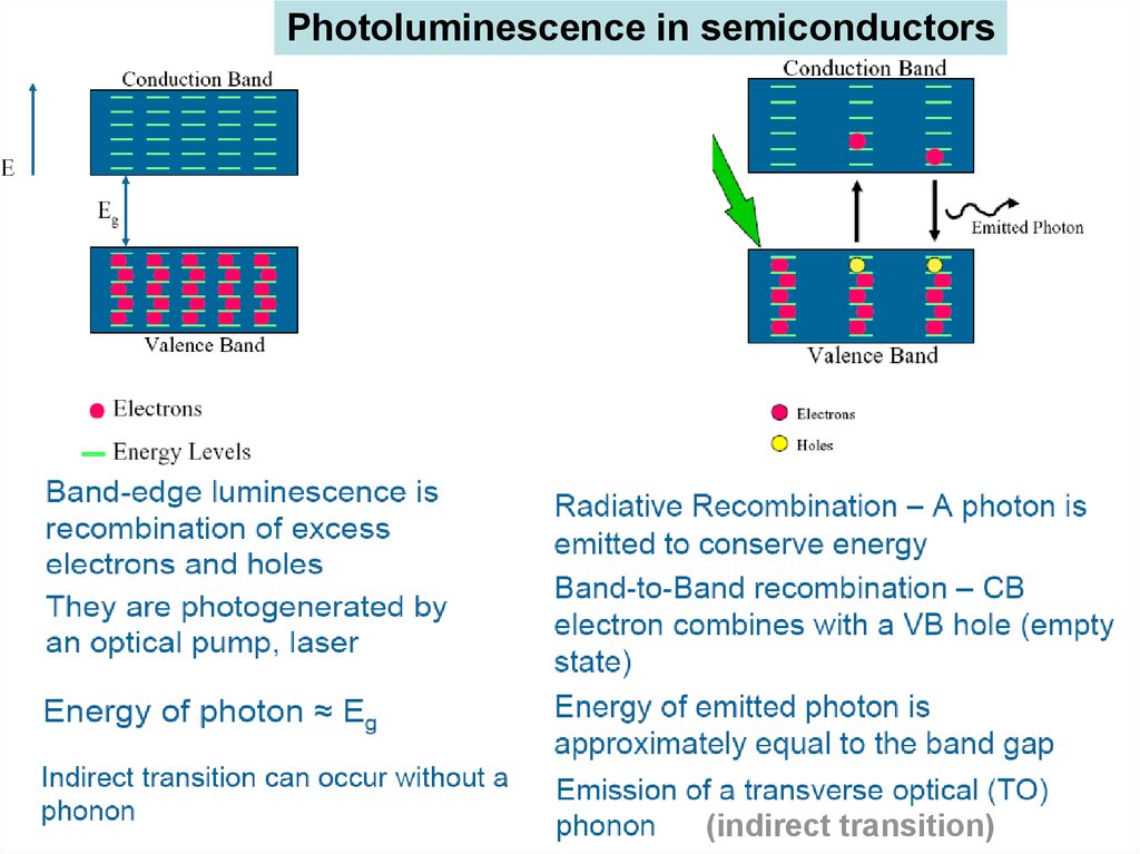
47. Luminescence
•Luminescence : Emission of radiation in excess of theamount emitted in thermal Equilibrium (Non equilibrium
phenomenon)
•Needs to create excess electrons and holes
•Electron-hole recombination => luminescence
If the emission is fast (<10-8 sec) – Fluorescent
Slow emission process --- Phosphorescent
48.
Photoluminescence in semiconductors(indirect transition)
49.
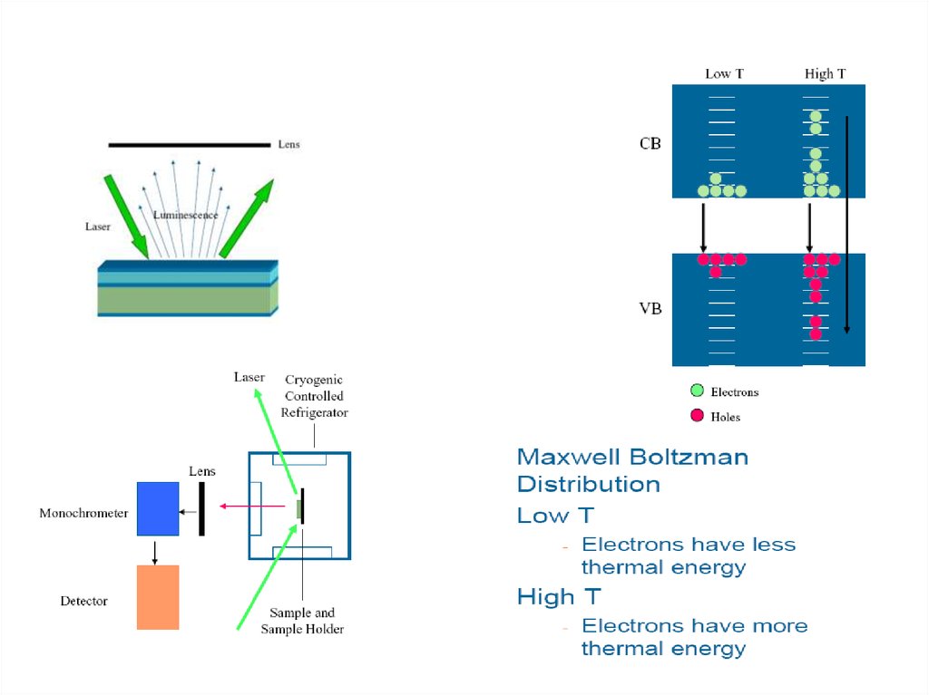
50. PL spectrum of a semiconductor
Reduced peak width atlow temperature
Photoluminescence intensity is
related to Temperature
51.
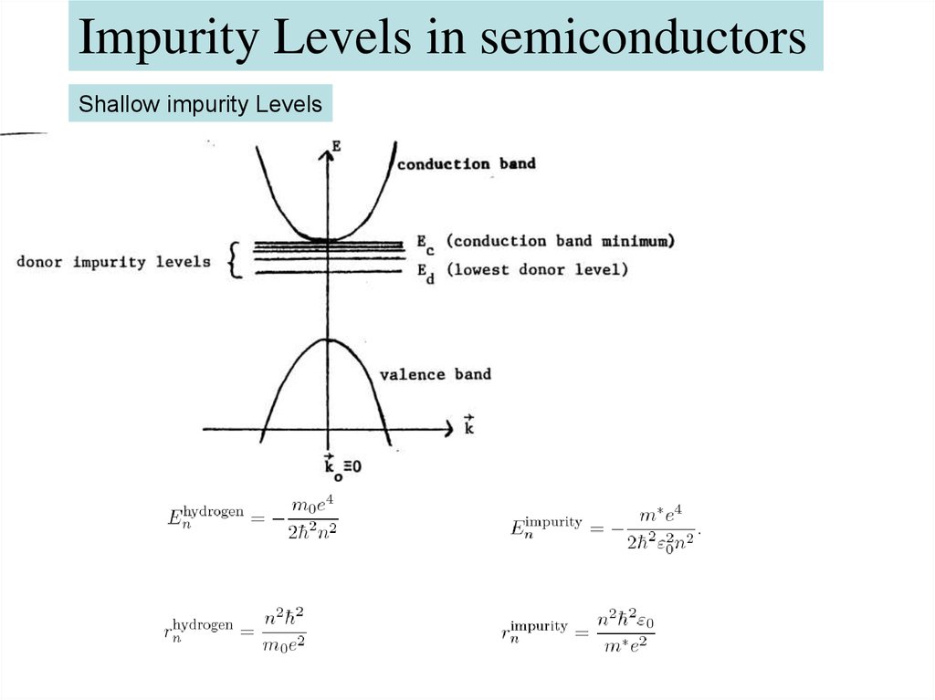
Impurity Levels in semiconductorsShallow impurity Levels
52. Excitons
•Electrons and holes bound together by their CoulombInteraction
•Important at low temperatures
LEDs and semiconductor lasers
•Created by photons with energy slightly less than Eg
53. Interaction of Electrons, X-rays, and Neutrons with matter
54.
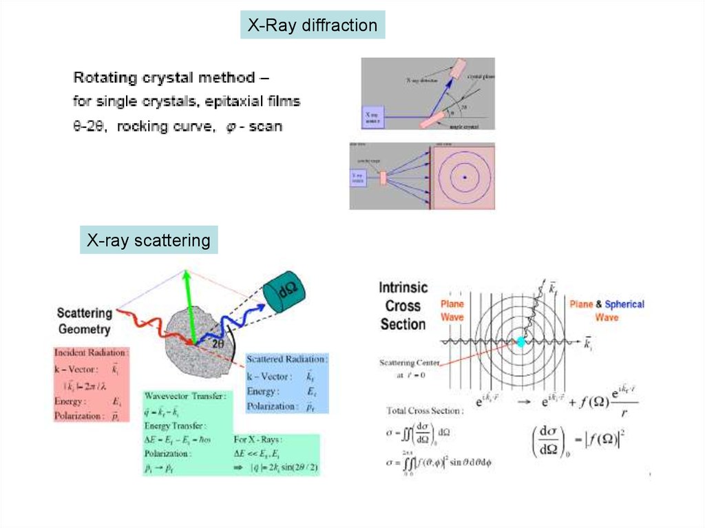
X-Ray diffractionX-ray scattering