Similar presentations:
Changes to LPDIMM Rev 02_r1
1. Changes to LPDIMM Rev 02
2. 1. general
• A. Please fix all dangling via and wherepossible fix Antena via (47 Dangling, 620
Antena). – one dangling line lef
• B. clean unneeded shapes.
• C. move vias in all design so they will not be
on shape’s edge (example in section 6)
3. 2. Component: nets in all design
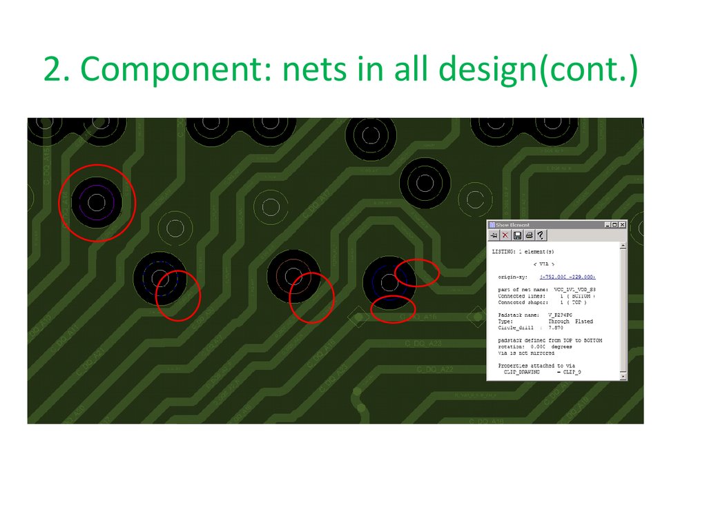
• Please fix all places where nets are routed tooclose (touching) in voids of the reference plane
above it or beneath.
• In the pic at following page, there is example of
this case in L3 routing, with reference in
L2_GND.
• It is wanted that lines will be far from these
voids 1W (one signal width), but at least not
touching if 1W is not possible.
4. 2. Component: nets in all design(cont.)
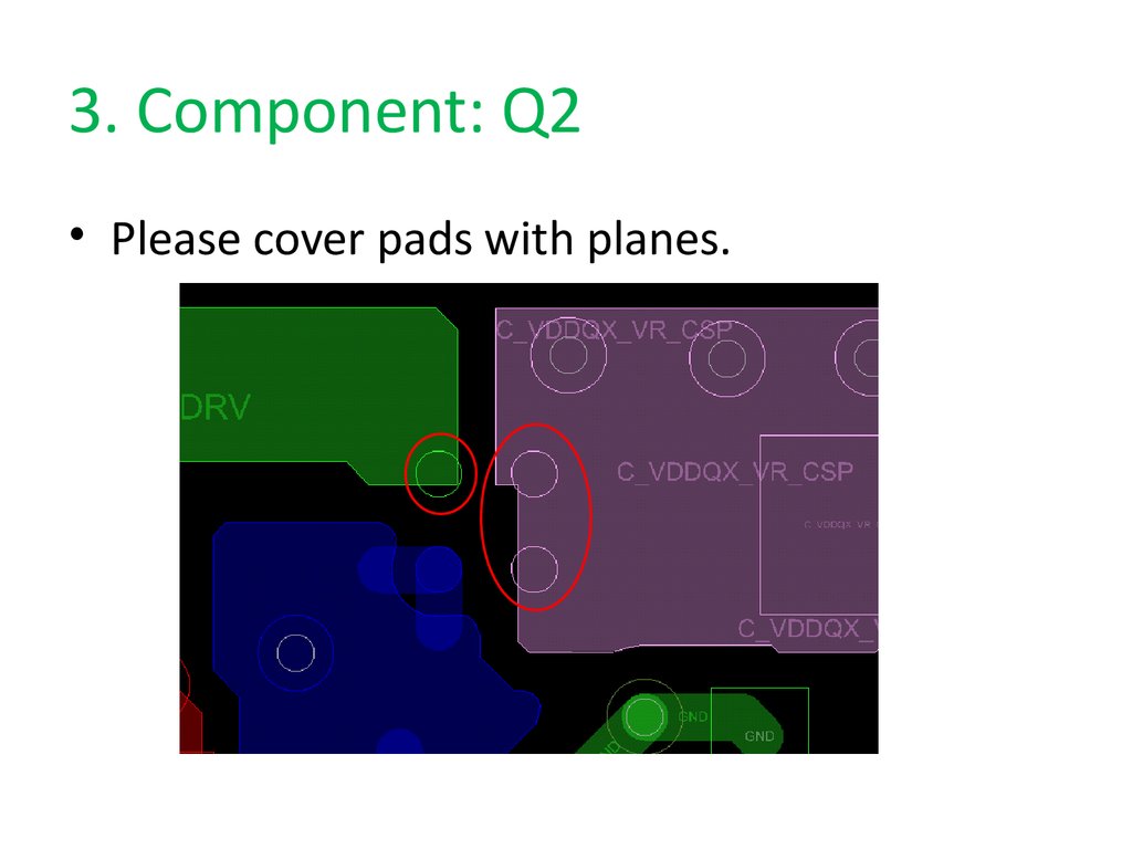
5. 3. Component: Q2
• Please cover pads with planes.6. 4. Component: U9
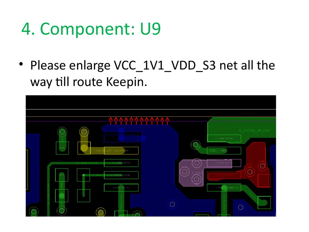
• Please enlarge VCC_1V1_VDD_S3 net all theway till route Keepin.
7. 5. New MASK for VIA_FILL
• Please prepare new mask called VIA_FILL.• This mask will contain all vias only in the
DRAM BGA TOP layer.
8. 6. Top layer
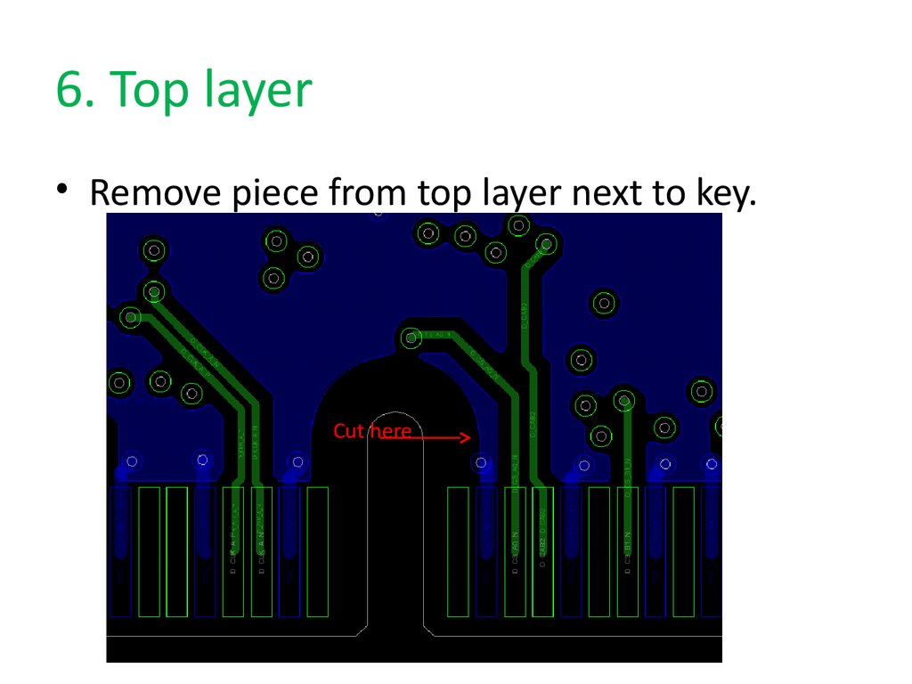
• Remove piece from top layer next to key.Cut here
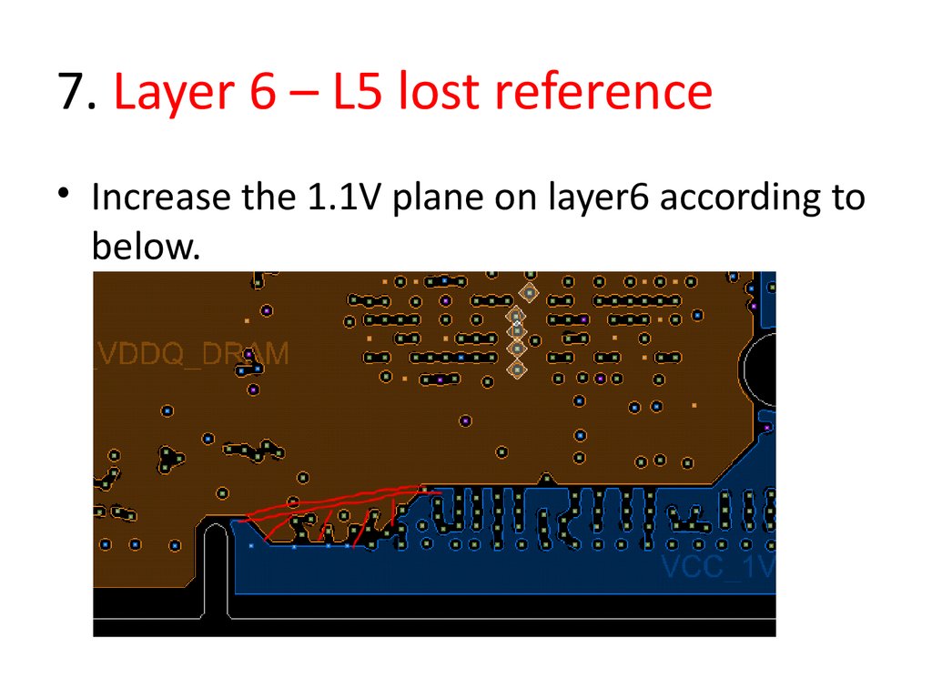
9. 7. Layer 6 – L5 lost reference
• Increase the 1.1V plane on layer6 according tobelow.
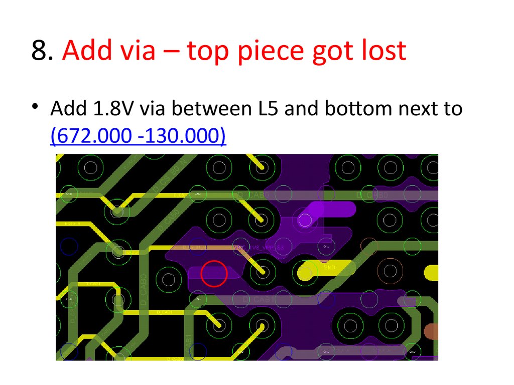
10. 8. Add via – top piece got lost
• Add 1.8V via between L5 and bottom next to(672.000 -130.000)
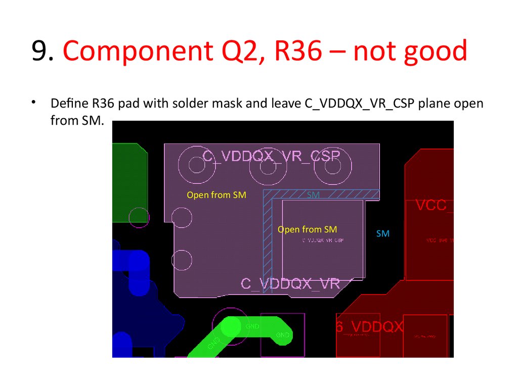
11. 9. Component Q2, R36 – not good
Define R36 pad with solder mask and leave C_VDDQX_VR_CSP plane open
from SM.
Open from SM
SM
Open from SM
SM
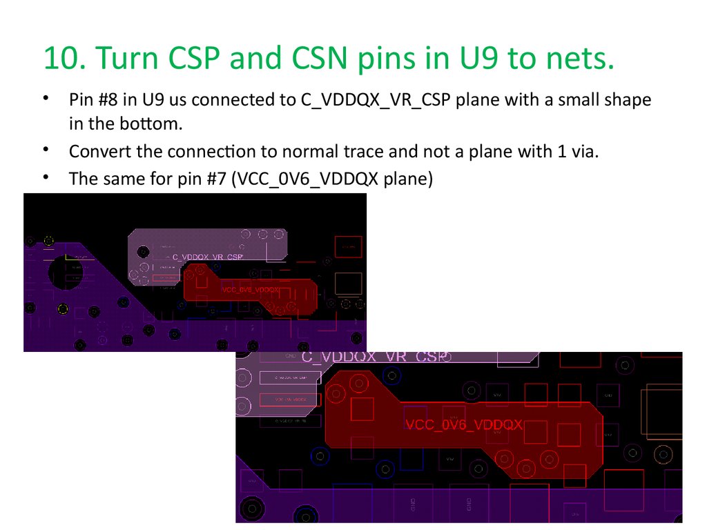
12. 10. Turn CSP and CSN pins in U9 to nets.
Pin #8 in U9 us connected to C_VDDQX_VR_CSP plane with a small shape
in the bottom.
Convert the connection to normal trace and not a plane with 1 via.
The same for pin #7 (VCC_0V6_VDDQX plane)
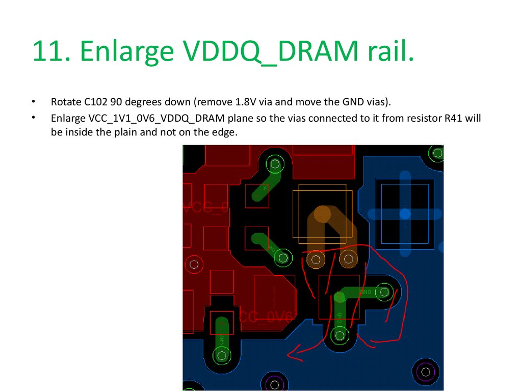
13. 11. Enlarge VDDQ_DRAM rail.
Rotate C102 90 degrees down (remove 1.8V via and move the GND vias).
Enlarge VCC_1V1_0V6_VDDQ_DRAM plane so the vias connected to it from resistor R41 will
be inside the plain and not on the edge.
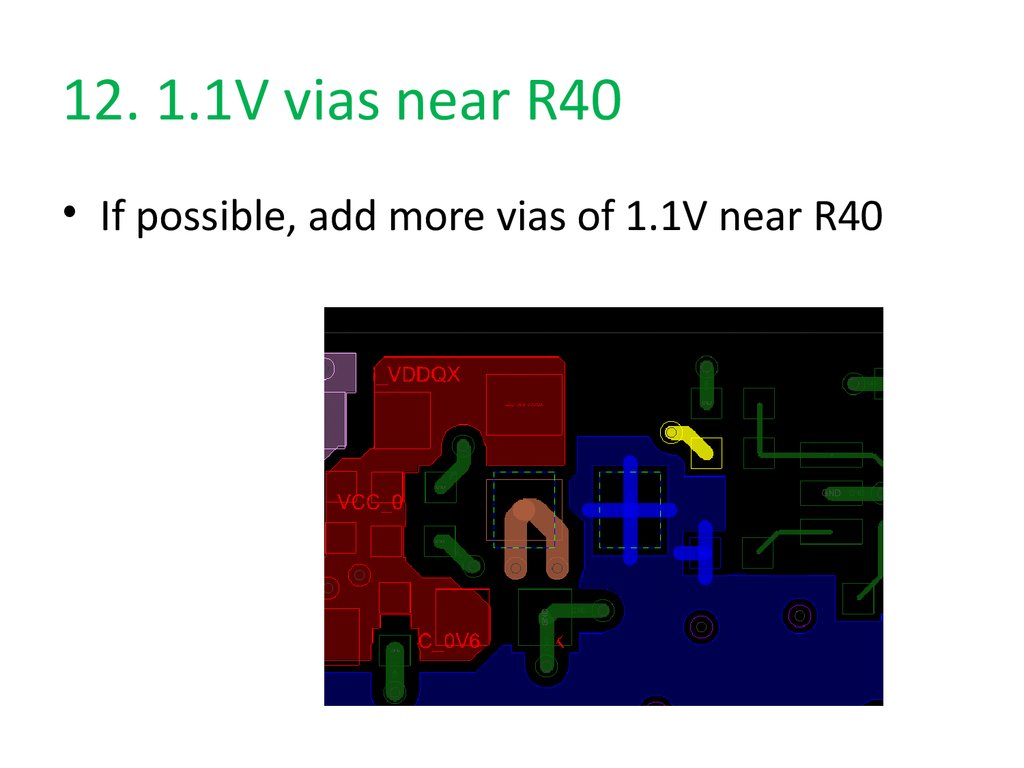
14. 12. 1.1V vias near R40
• If possible, add more vias of 1.1V near R4015. 13. 1.1V/VPP TP
• Route a trace from DRAM to 1.1V and VPP TPinstead of direct connection to the plane.
• If impossible, try at least to do that for 1.1V
(TP11 and TP15)
16. 14. Silk - TOP
• Fix REFDES for new components. And oldcomponents that moved.
• Fix silk of TP that moved.
• Change card name (LPDIMM_LP4_200B) to:
LP4/x_200B (CNL U) – move to Bottom.
17. 15. Silk – BOTTOM – space between 01 and ASSY
• Change PCB PN to: J24748-001 (leave Rev 01).• Change ASSY PN to: J24748-100
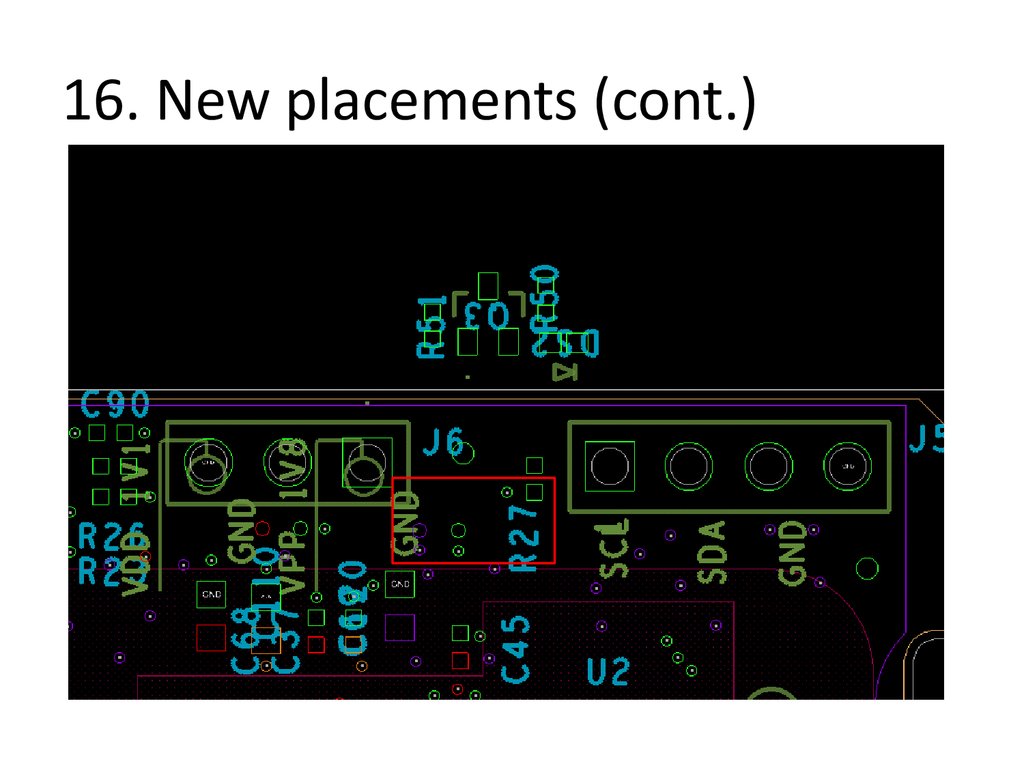
18. 16. New placement
The next slide shows basic placement.
Please move: TP17, TP18, J6, R27.
Please move J5 (4 pin header) a little to the right.
Place new components in the red square area.
• It doesn’t have to be exactly like I requested. It
can be changed a little bit as long as everything
fit.

