Similar presentations:
МЭМС и НЭМС: датчики ускорения и поворота, наноприводы, оптические и электронные системы
1. Наномеханика Nanomechanics of materials and systems
Лекции 14МЭМС и НЭМС:
датчики ускорения и поворота,
наноприводы, оптические и электронные
системы
MEMS and NEMS sensors of acceleration
and rotation, actuators, optical and electronic
systems
2. Базовая структура датчика ускорения Base structure of acceleration sensor
(stiffness)The basic structure of an accelerometer, consisting of an inertial mass
suspended from a spring. The resonant frequency and the noise-equivalent
acceleration (due to Brownian noise) are given.
3. Пьезорезистивный датчик ускорения Piezoresistive acceleration sensor
Illustration of a piezoresistive accelerometer from Endevco Corp., fabricated using anisotropicetching in a {110} wafer. The middle core contains the inertial mass suspended from a hinge.
Two piezoresistive sense elements measure the deflection of the mass. The axis of sensitivity is
in the plane of the middle core. The outer frame acts as a stop mechanism to prevent excessive
accelerations from damaging the part. fr=28 kHz. The piezoresistors are 0.6 μm thick and 4.2 μm
long, aligned along <111> direction for maximum performance. The output in response to an
acceleration of 1G is 25mV for a Wheatstone bridge excitation of 10V.
4. Емкостной датчик Capacitive sensor
Поперечная конфигурацияΔx
U Q / C; U Q C / C 2 U C / C
C
x0
Продольная конфигурация
C
x
x
l y l z
C
x ( x0 x ) 2
U Q l y l z / x
U U x /( x0 x )
Δy
ly
C (l y y )l z / x0
C yl z / x0
U U y /( l y y )
5. Емкостной датчик ускорения. Capacitive accelerometer.
Illustration of a bulk micromachined capacitive accelerometer. The inertial mass in the middle waferforms the moveable electrode of a variable differential capacitive circuit. Electronic circuits sense
changes in capacitance, then convert them into an output voltage between 0 and 5V. The rated
bandwidth is up to 400 Hz for the ±12G accelerometer, the cross-axis sensitivity is less than 5% of
output, and the shock immunity is 20,000G. Measuring range is from ±0.5G to ±12G. (VTI
Technologies of Vantaa, Finland.)
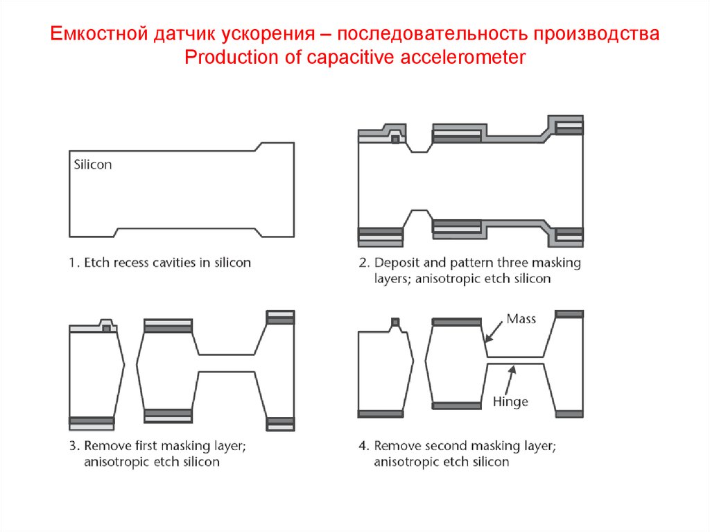
6. Емкостной датчик ускорения – последовательность производства Production of capacitive accelerometer
7. Емкостной датчик ускорения. Capacitive accelerometer.
Acceleration ratingis from 1G to 100 G,
excitation frequency is
1 MHz, C = 10-13F
bandwidth is 1-6 kHz,
mass is 0.3 - 100 μg,
Brownian mechanical
noise for 0.3 μg is 225
μG Hz1/2
Illustration of the basic structure of the ADXL family of surface micromachined
accelerometers. A comb-like structure suspended from springs forms the inertial mass.
Displacements of the mass are measured capacitively with respect to two sets of stationary
finger-like electrodes. (Analog Devices, Inc., Norwood, Massachusetts, USA.)
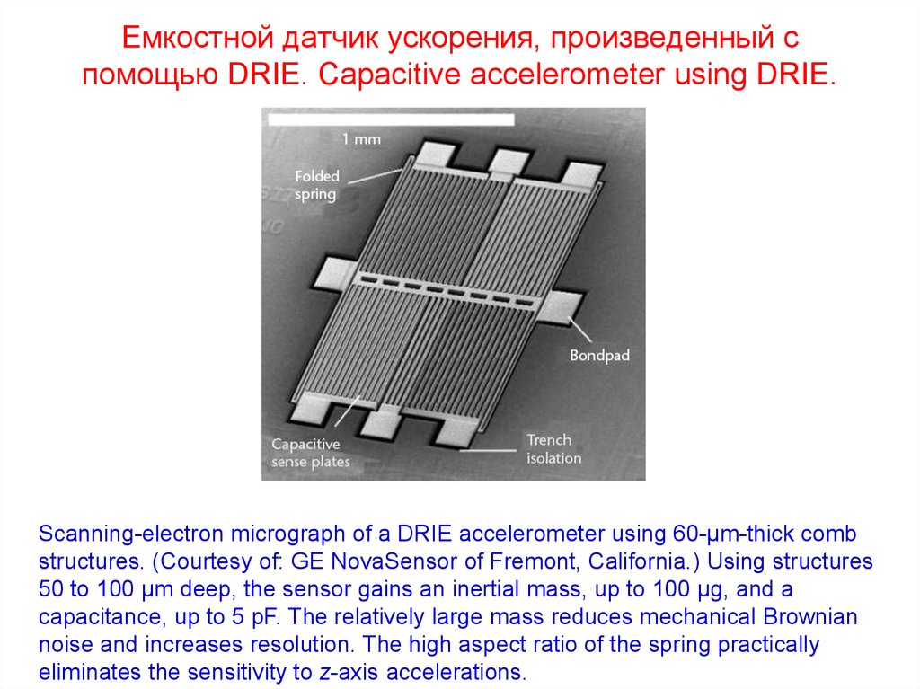
8. Емкостной датчик ускорения, произведенный с помощью DRIE. Capacitive accelerometer using DRIE.
Scanning-electron micrograph of a DRIE accelerometer using 60-μm-thick combstructures. (Courtesy of: GE NovaSensor of Fremont, California.) Using structures
50 to 100 μm deep, the sensor gains an inertial mass, up to 100 μg, and a
capacitance, up to 5 pF. The relatively large mass reduces mechanical Brownian
noise and increases resolution. The high aspect ratio of the spring practically
eliminates the sensitivity to z-axis accelerations.
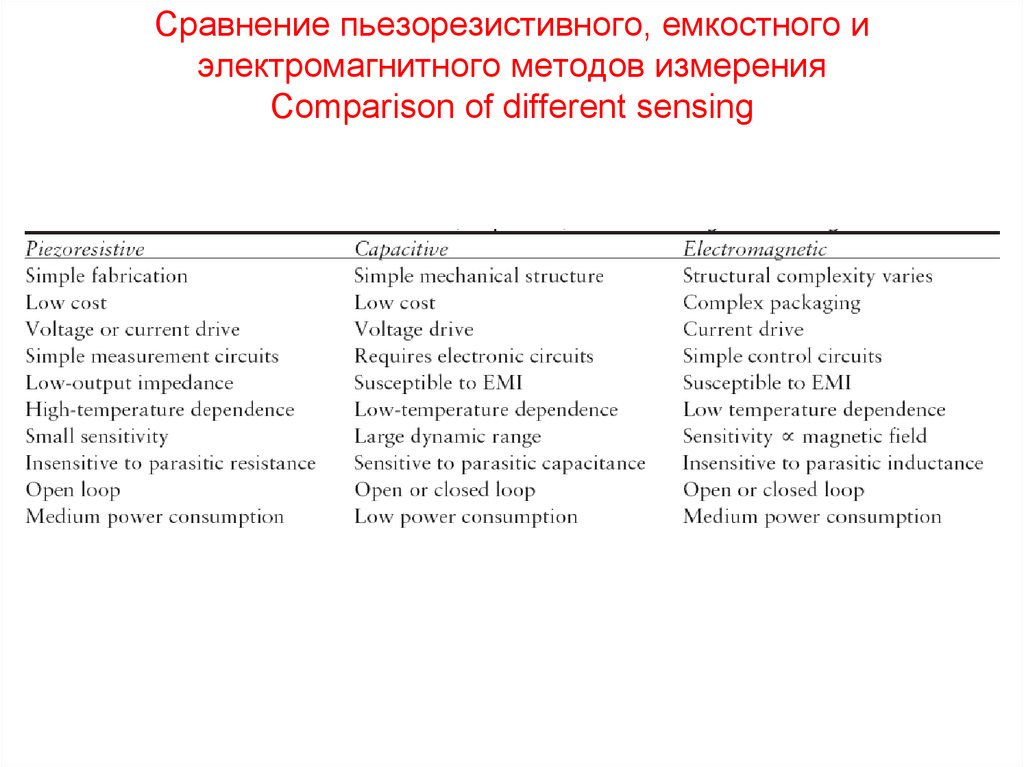
9. Сравнение пьезорезистивного, емкостного и электромагнитного методов измерения Comparison of different sensing
10. Элементы НЭМС NEMS elements
• Пассивные Passive• Датчики Sensors
• Приводы (актуаторы) Actuators
11. Термический привод Thermal actuator
if F is the external force12. Пьезоэлектрический элемент (датчик или привод) Piezoelectric sensor and actuator
Активный элемент:ZnO, LiNbO3, BaTiO3,
PbZrO3 или кварц
An illustration of the piezoelectric effect on a
crystalline plate. An applied voltage
across the electrodes results in dimensional changes
in all three axes (if d31 and d33 are nonzero).
Conversely, an applied force in any of three directions
gives rise to a measurable voltage across the
electrodes.
13. Электростатический нанопривод Electrostatic actuator
zx
F
U
y0 z0V
x ( x0 x )2
U
z0V 2
F
n
y
2x0
2
F
Δx/x
(a) An illustration of a parallel-plate electrostatic actuator with an
applied voltage V and a spacing x. The attractive force is normal to the
plate surfaces. (b) An illustration of an electrostatic comb actuator. The
attractive force is in the direction of the interdigitated teeth.
y
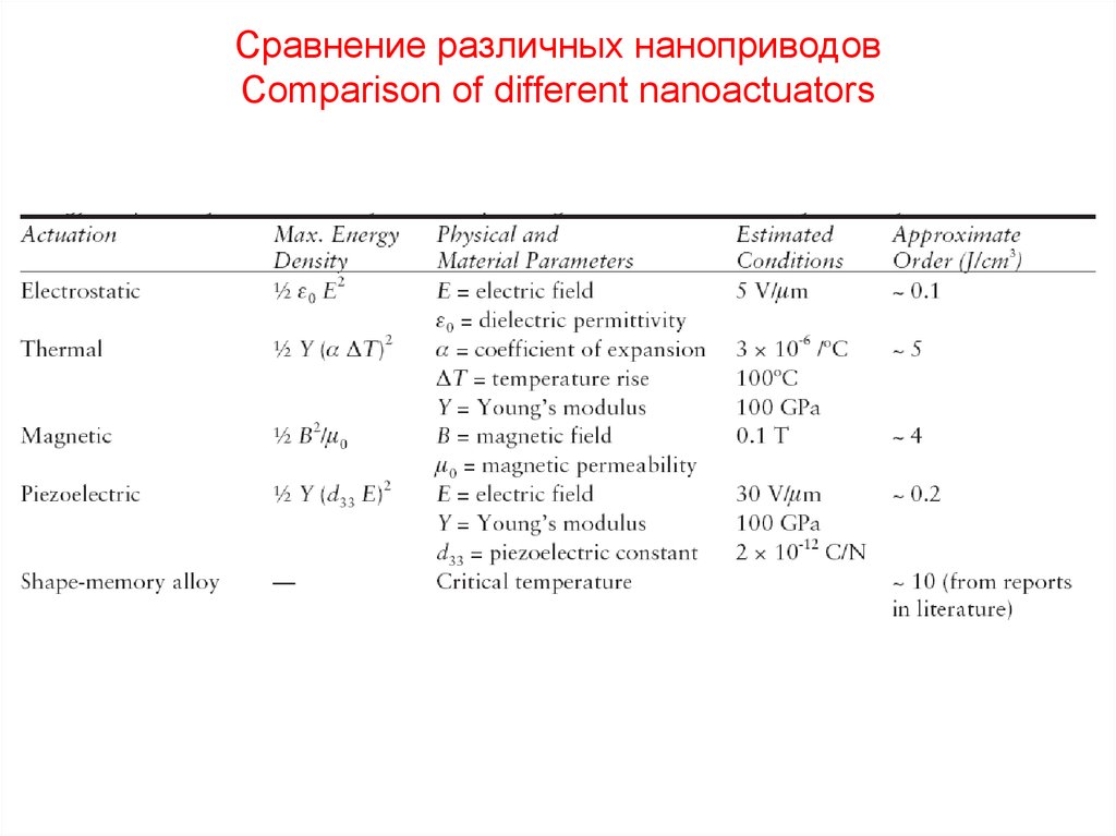
14. Сравнение различных наноприводов Comparison of different nanoactuators
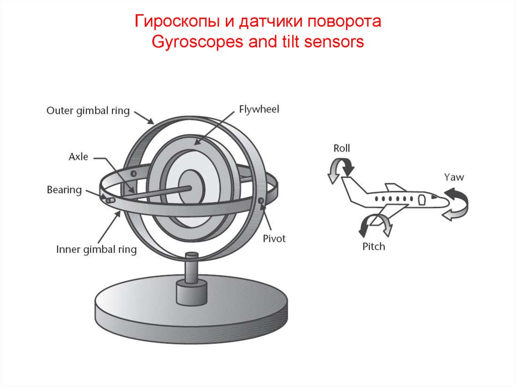
15. Гироскопы и датчики поворота Gyroscopes and tilt sensors
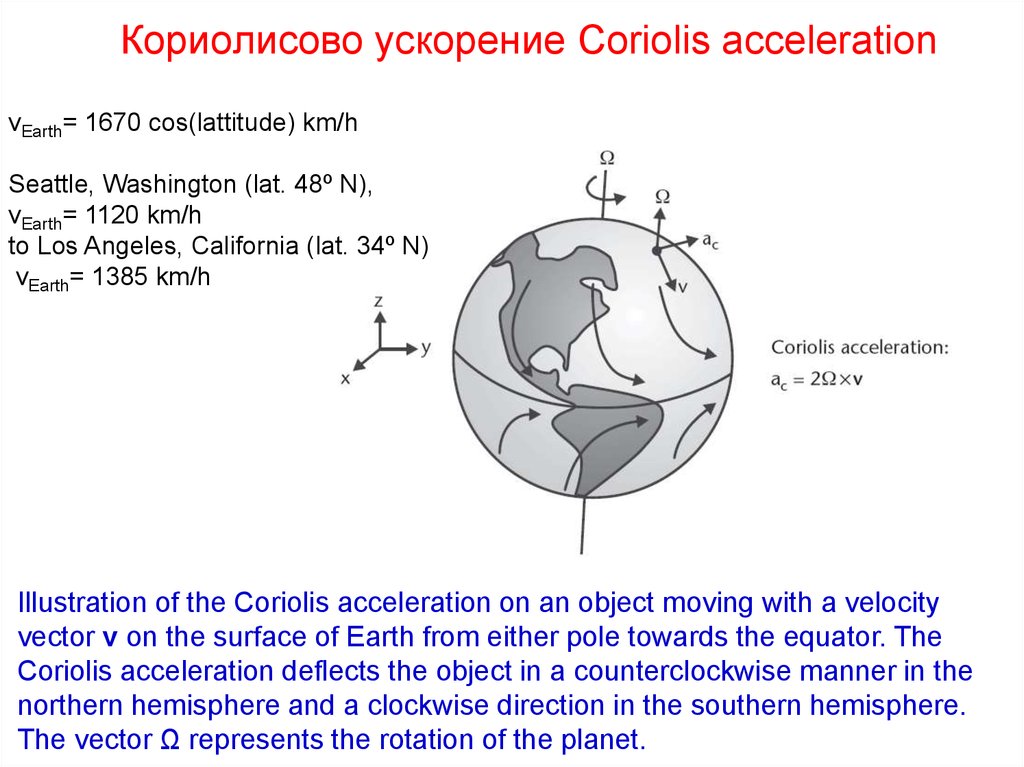
16. Кориолисово ускорение Coriolis acceleration
vEarth= 1670 cos(lattitude) km/hSeattle, Washington (lat. 48º N),
vEarth= 1120 km/h
to Los Angeles, California (lat. 34º N)
vEarth= 1385 km/h
Illustration of the Coriolis acceleration on an object moving with a velocity
vector v on the surface of Earth from either pole towards the equator. The
Coriolis acceleration deflects the object in a counterclockwise manner in the
northern hemisphere and a clockwise direction in the southern hemisphere.
The vector Ω represents the rotation of the planet.
17. Базовый датчик угловой скорости Base angular rate sensor
Illustration of the tuning-fork structure for angular-ratesensing. The Coriolis effect transfers energy from a
primary flexural mode to a secondary torsional mode.
Coriolis acceleration ac = 2Ω x v.
18. Датчик угловой скорости Angular-rate sensor
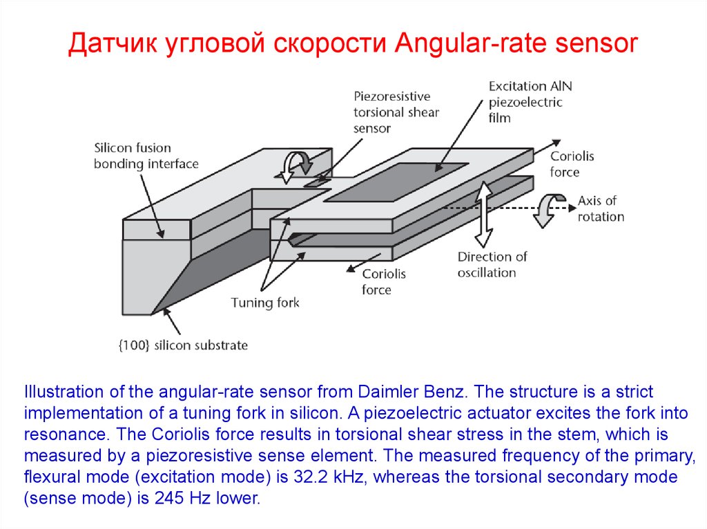
Illustration of the angular-rate sensor from Daimler Benz. The structure is a strictimplementation of a tuning fork in silicon. A piezoelectric actuator excites the fork into
resonance. The Coriolis force results in torsional shear stress in the stem, which is
measured by a piezoresistive sense element. The measured frequency of the primary,
flexural mode (excitation mode) is 32.2 kHz, whereas the torsional secondary mode
(sense mode) is 245 Hz lower.
19. Датчик угловой скорости Daimler Benz – последовательность производства Angular-rate sensor – fabrication steps
20. Датчик угловой скорости Angular-rate sensor
Illustration of the Delphi Delcoangular-rate sensor and the
corresponding standing-wave
pattern. The basic structure
consists of a ring shell
suspended from an anchor by
support flexures. A total of 32
electrodes (only a few are
shown) distributed around the
entire perimeter of the ring
excite a primary mode of
resonance using electrostatic
actuation. A second set of
distributed electrodes
capacitively sense the
vibration modes. The angular
shift of the standing-wave
pattern is a measure of the
angular velocity.
21. Датчик угловой скорости Angular-rate sensor
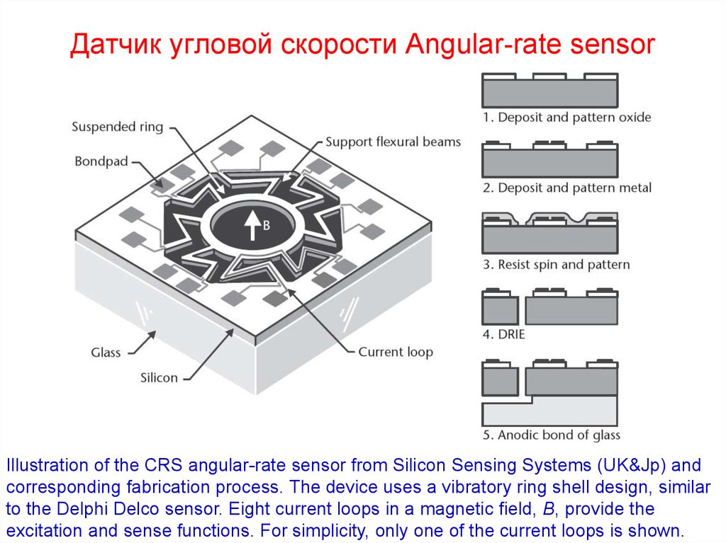
Illustration of the CRS angular-rate sensor from Silicon Sensing Systems (UK&Jp) andcorresponding fabrication process. The device uses a vibratory ring shell design, similar
to the Delphi Delco sensor. Eight current loops in a magnetic field, B, provide the
excitation and sense functions. For simplicity, only one of the current loops is shown.
22. Микро/наногенераторы: Vibration Harvesting
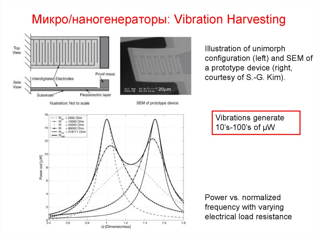
Illustration of unimorphconfiguration (left) and SEM of
a prototype device (right,
courtesy of S.-G. Kim).
Vibrations generate
10’s-100’s of μW
Power vs. normalized
frequency with varying
electrical load resistance
23. Self-powered Wireless Corrosion-monitoring System
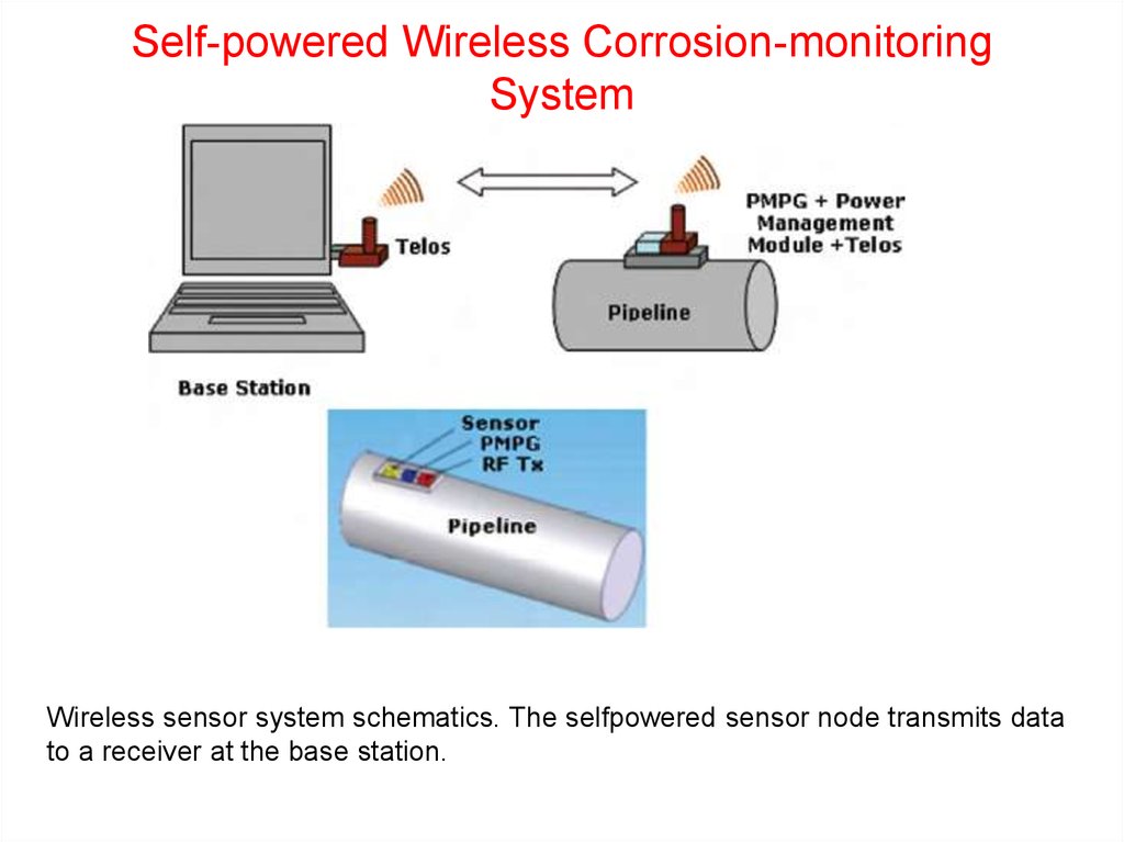
Wireless sensor system schematics. The selfpowered sensor node transmits datato a receiver at the base station.
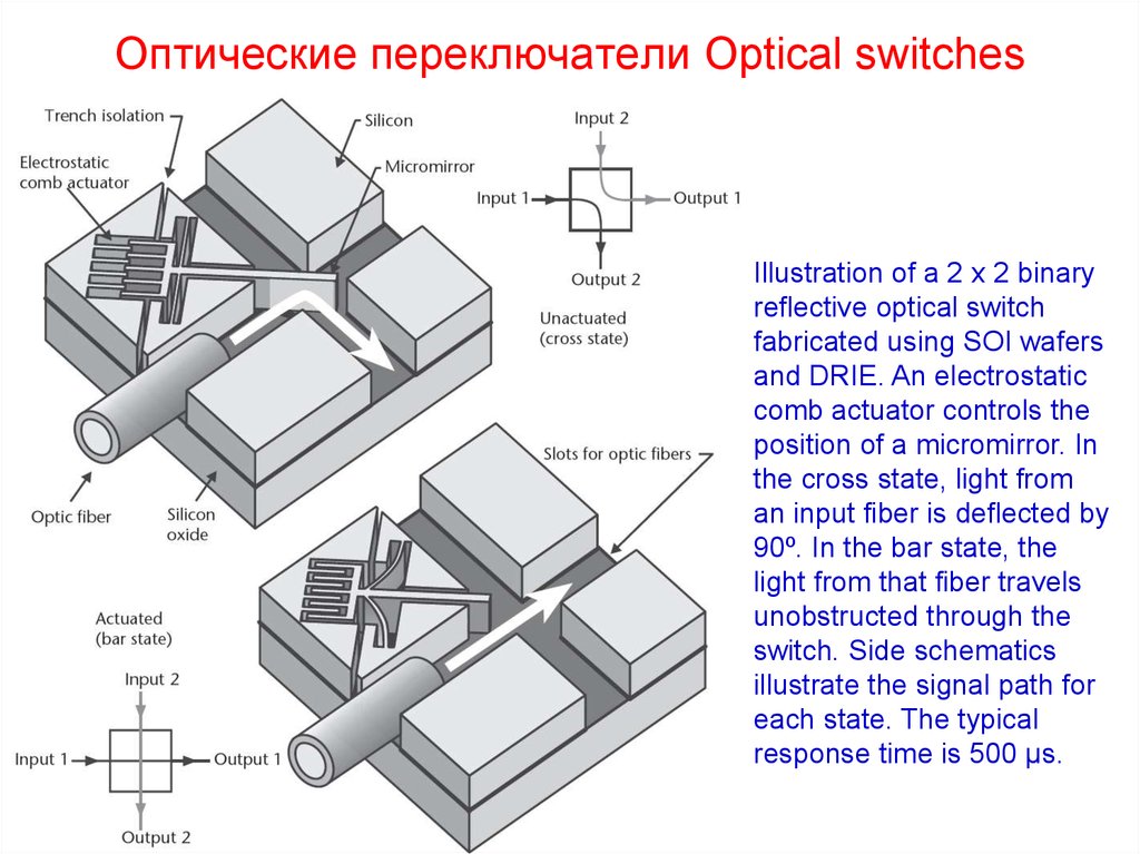
24. Оптические переключатели Optical switches
Illustration of a 2 x 2 binaryreflective optical switch
fabricated using SOI wafers
and DRIE. An electrostatic
comb actuator controls the
position of a micromirror. In
the cross state, light from
an input fiber is deflected by
90º. In the bar state, the
light from that fiber travels
unobstructed through the
switch. Side schematics
illustrate the signal path for
each state. The typical
response time is 500 μs.
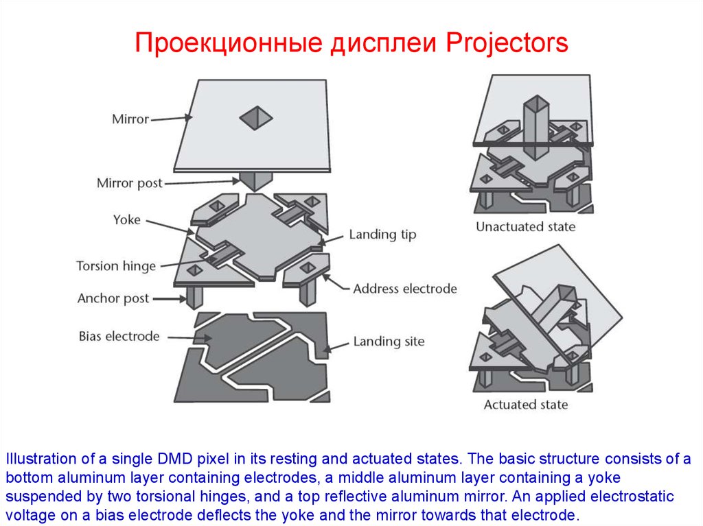
25. Проекционные дисплеи Projectors
Illustration of a single DMD pixel in its resting and actuated states. The basic structure consists of abottom aluminum layer containing electrodes, a middle aluminum layer containing a yoke
suspended by two torsional hinges, and a top reflective aluminum mirror. An applied electrostatic
voltage on a bias electrode deflects the yoke and the mirror towards that electrode.
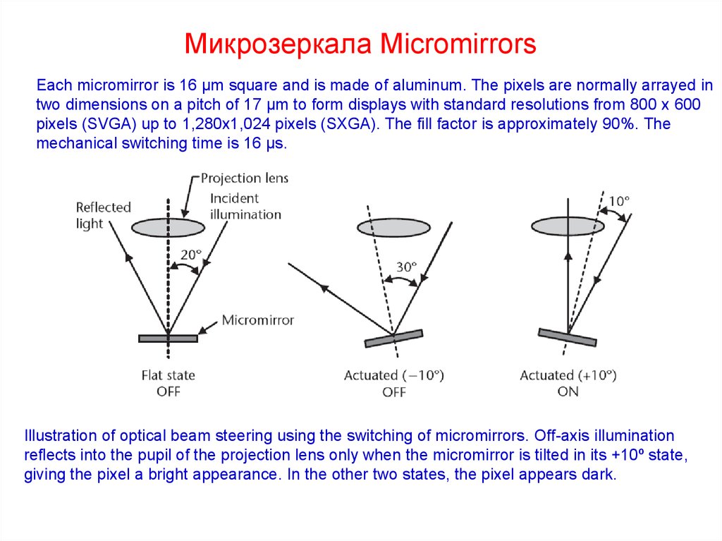
26. Микрозеркалa Micromirrors
Each micromirror is 16 μm square and is made of aluminum. The pixels are normally arrayed intwo dimensions on a pitch of 17 μm to form displays with standard resolutions from 800 x 600
pixels (SVGA) up to 1,280x1,024 pixels (SXGA). The fill factor is approximately 90%. The
mechanical switching time is 16 μs.
Illustration of optical beam steering using the switching of micromirrors. Off-axis illumination
reflects into the pupil of the projection lens only when the micromirror is tilted in its +10º state,
giving the pixel a bright appearance. In the other two states, the pixel appears dark.
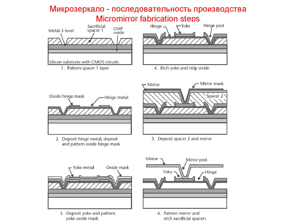
27. Микрозеркало - последовательность производства Micromirror fabrication steps
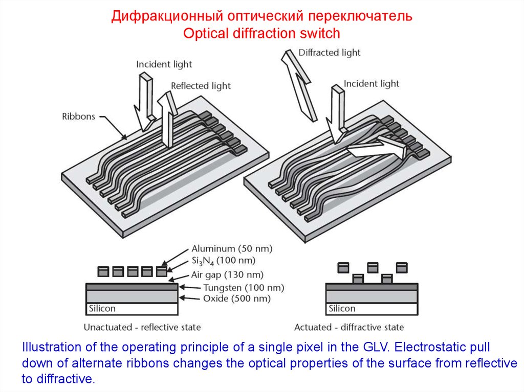
28. Дифракционный оптический переключатель Optical diffraction switch
Illustration of the operating principle of a single pixel in the GLV. Electrostatic pulldown of alternate ribbons changes the optical properties of the surface from reflective
to diffractive.
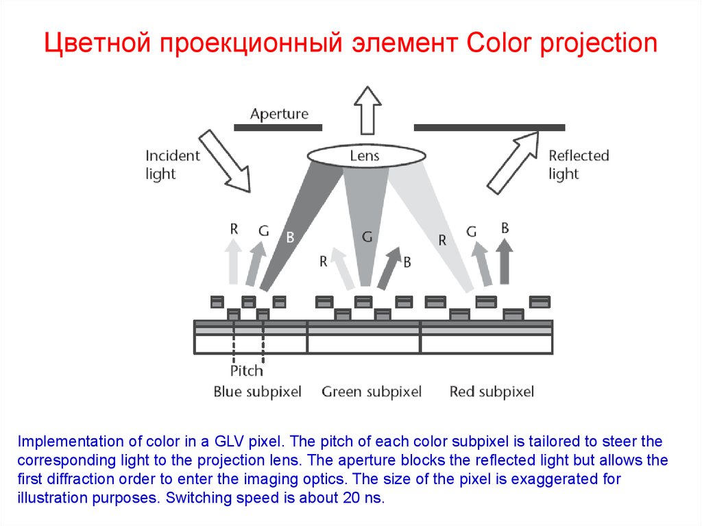
29. Цветной проекционный элемент Color projection
Implementation of color in a GLV pixel. The pitch of each color subpixel is tailored to steer thecorresponding light to the projection lens. The aperture blocks the reflected light but allows the
first diffraction order to enter the imaging optics. The size of the pixel is exaggerated for
illustration purposes. Switching speed is about 20 ns.
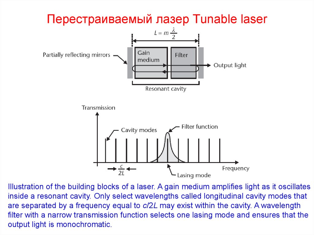
30. Перестраиваемый лазер Tunable laser
Illustration of the building blocks of a laser. A gain medium amplifies light as it oscillatesinside a resonant cavity. Only select wavelengths called longitudinal cavity modes that
are separated by a frequency equal to c/2L may exist within the cavity. A wavelength
filter with a narrow transmission function selects one lasing mode and ensures that the
output light is monochromatic.
31. Внешний резонатор для перестраиваемого лазера External resonator for a tunable laser
(a) Illustration of the Littman-Metcalf external cavity laser configuration. Light from the laser diode iscollimated and diffracted by a grating acting as a wavelength filter. Lasing occurs only at one
wavelength, whose diffraction order is reflected by the mirror back into the cavity. (b) Rotating the
mirror around a virtual pivot point changes the wavelength and tunes the laser.
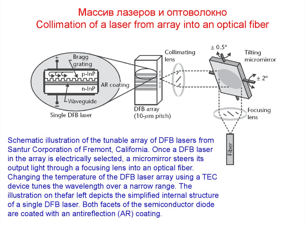
32. Массив лазеров и оптоволокно Collimation of a laser from array into an optical fiber
Schematic illustration of the tunable array of DFB lasers fromSantur Corporation of Fremont, California. Once a DFB laser
in the array is electrically selected, a micromirror steers its
output light through a focusing lens into an optical fiber.
Changing the temperature of the DFB laser array using a TEC
device tunes the wavelength over a narrow range. The
illustration on thefar left depicts the simplified internal structure
of a single DFB laser. Both facets of the semiconductor diode
are coated with an antireflection (AR) coating.
33. Микрозеркало Micromirror
Schematic cross section of the micromirror used within the tunable laser from SanturCorporation. The device consists of a double-gimbaled mirror structure supported by
torsional hinges. A gold layer defines the high-reflectivity mirror surface that remains at
ground potential. Four gold electrodes on an anodically bonded glass substrate actuate
the mirror and cause rotation around the hinges.
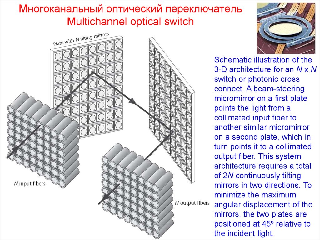
34. Многоканальный оптический переключатель Multichannel optical switch
Schematic illustration of the3-D architecture for an N x N
switch or photonic cross
connect. A beam-steering
micromirror on a first plate
points the light from a
collimated input fiber to
another similar micromirror
on a second plate, which in
turn points it to a collimated
output fiber. This system
architecture requires a total
of 2N continuously tilting
mirrors in two directions. To
minimize the maximum
angular displacement of the
mirrors, the two plates are
positioned at 45º relative to
the incident light.
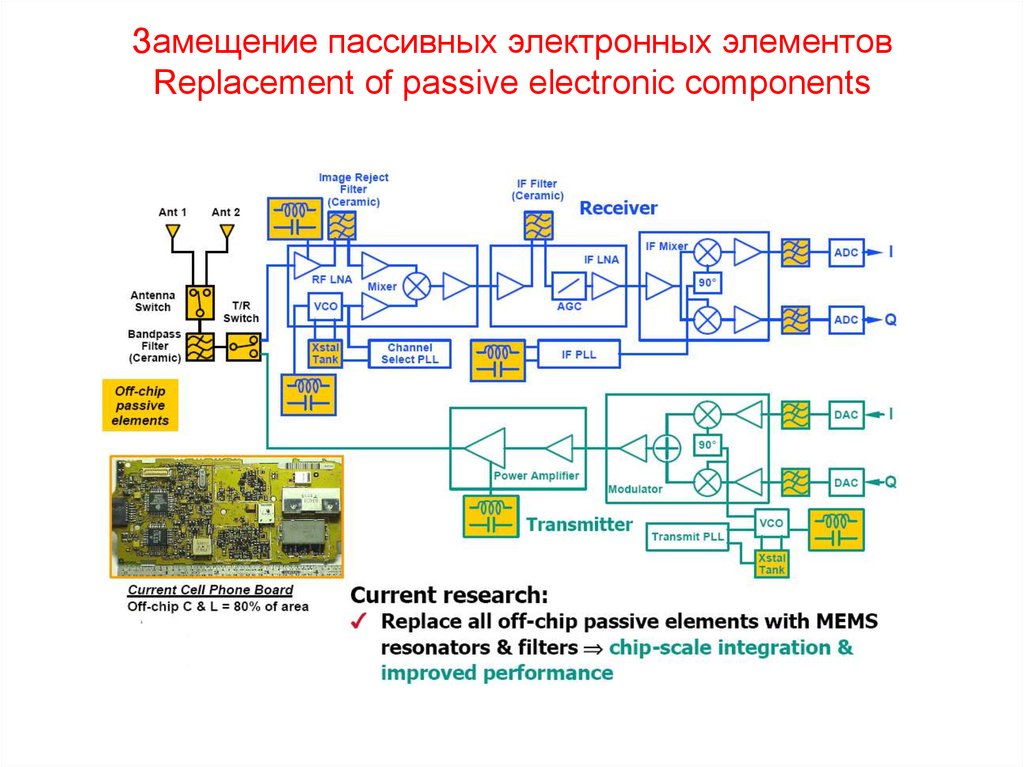
35. Замещение пассивных электронных элементов Replacement of passive electronic components
36. Индуктивность Microinductor
The PARC inductor: (a) scanning-electron micrograph (SEM) of a five-turnsolenoid inductor (the locations of the sides of the turns before release are
visible); and (b) SEM close up of the tops of the turns where the metal from
each side meets, showing the interlocked ends. The etch holes have been
filled with copper.
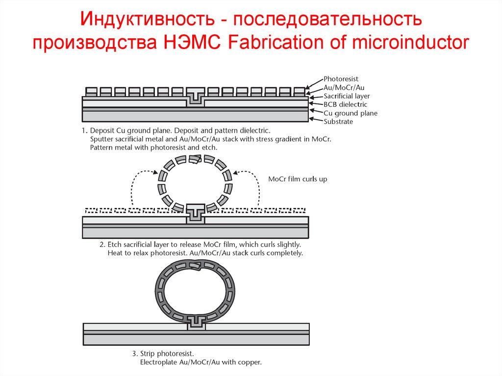
37. Индуктивность - последовательность производства НЭМС Fabrication of microinductor
38. Переменная емкость Tunable capacitor
39. Резонатор Resonator
Добротность Qкварц Q≈10000
RLC Q<1000
НЭМС:
вакуум Q>50000
воздух Q<50
k = E t (w/L)3
E = 160 GPa
t = 2 μm
w = 2 μm
L = 33 μm
m = 5.7 10-11 kg
f = 190 kHz
Illustration of a micromachined folded-beam comb-drive resonator. The left comb drive actuates the
device at a variable frequency ω. The right capacitive-sense-comb structure measures the
corresponding displacement by turning the varying capacitance into a current, which generates a
voltage across the output resistor. There is a peak in displacement, current, and output voltage at
the resonant frequency.
40. Высокочастотный резонатор с термокомпенсацией Resonator with thermal compensation
Illustration of the compensation scheme to reduce sensitivity in a resonant structure to temperature.A voltage applied to a top metal electrode modifies through electrostatic attraction the effective
spring constant of the resonant beam. Temperature changes cause the metal electrode to move
relative to the polysilicon resonant beam, thus changing the gap between the two layers. This
reduces the electrically induced spring constant opposing the mechanical spring while the
mechanical spring constant itself is falling, resulting in their combination varying much less with
temperature. (a) Perspective view of the structure, and (b) scanning electron micrograph of the
device. (Courtesy of: Discera, Inc., Ann Arbor, Michigan, USA.)
41. Переключатель Electric switch
Shock tolerance of30,000G,
insertion loss of
0.2 dB over 24–40 GHz,
open isolation of
40 dB,
lifetime of
1011 cycles,
cold-switched power of
1-W
MicroAssembly Technologies of Richmond, California, USA













 physics


