Similar presentations:


")


")

Problems-of-Modern-Photolithography
1.
Problems of ModernPhotolithography
On the Path to Physical Limits
Good morning, everyone. Today, we delve into the critical challenges facing
modern photolithography, the cornerstone of semiconductor manufacturing.
As we push the boundaries of miniaturisation, we encounter significant
hurdles that demand innovative solutions. This presentation will explore
these problems and highlight the ingenious approaches being developed to
overcome them, ensuring the continued advancement of semiconductor
technology.
2.
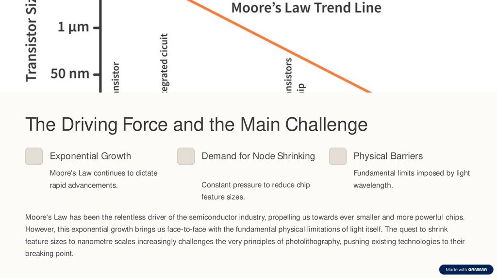
The Driving Force and the Main ChallengeExponential Growth
Demand for Node Shrinking
Moore's Law continues to dictate
rapid advancements.
Physical Barriers
Fundamental limits imposed by light
Constant pressure to reduce chip
wavelength.
feature sizes.
Moore's Law has been the relentless driver of the semiconductor industry, propelling us towards ever smaller and more powerful chips.
However, this exponential growth brings us face-to-face with the fundamental physical limitations of light itself. The quest to shrink
feature sizes to nanometre scales increasingly challenges the very principles of photolithography, pushing existing technologies to their
breaking point.
3.
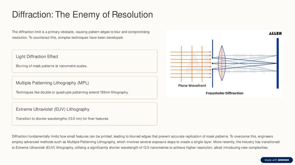
Diffraction: The Enemy of ResolutionThe diffraction limit is a primary obstacle, causing pattern edges to blur and compromising
resolution. To counteract this, complex techniques have been developed.
Light Diffraction Effect
Blurring of mask patterns at nanometre scales.
Multiple Patterning Lithography (MPL)
Techniques like double or quadruple patterning extend 193nm lithography.
Extreme Ultraviolet (EUV) Lithography
Transition to shorter wavelengths (13.5 nm) for finer features.
Diffraction fundamentally limits how small features can be printed, leading to blurred edges that prevent accurate replication of mask patterns. To overcome this, engineers
employ advanced methods such as Multiple Patterning Lithography, which involves several exposure steps to create a single layer. More recently, the industry has transitioned
to Extreme Ultraviolet (EUV) lithography, utilising a significantly shorter wavelength of 13.5 nanometres to achieve higher resolution, albeit introducing new complexities.
4.
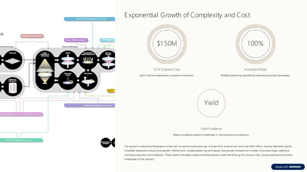
E xponential Growth of Complexity and Cost$1 50M
1 00%
E UV Scanner Cost
Increased Steps
Each machine represents a massive investment.
Multiple patterning significantly extends production processes.
Yield
Yield P roblems
Higher complexity leads to challenges in manufacturing consistency.
The pursuit of advanced lithography comes with an astronomical price tag. A single EUV scanner can cost over $150 million, making fabrication plants
incredibly expensive to build and operate. Furthermore, multiple patterning techniques dramatically increase the number of process steps, adding to
manufacturing time and complexity. These factors inevitably impact overall production yield and drive up the cost per chip, posing significant economic
challenges for the industry.
5.
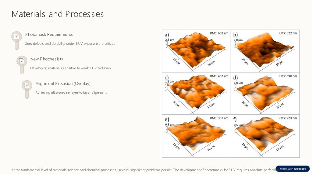
Materials and ProcessesP hotomask Requirements
Zero defects and durability under E UV exposure are critical.
New P hotoresists
Developing materials sensitive to weak E UV radiation.
Alignment P recision (Overlay)
Achieving ultra-precise layer-to-layer alignment.
At the fundamental level of materials science and chemical processes, several significant problems persist. The development of photomasks for E UV requires absolute perfection—zero
6.
Conclusions and HorizonsHitting Limits
E UV Not the E nd-All
Searching for Alternatives
Photolithography faces physical and
While advanced, EUV is not the ultimate
Exploring nanolithography and self-
economic boundaries.
solution.
assembly methods.
In summary, modern photolithography is rapidly approaching its physical and economic limits. While EUV lithography represents a monumental
leap, it is not the final answer to our patterning challenges. Future advancements will necessitate breakthroughs not only in lithographic techniques
but also in novel chip architectures. Research into fundamentally new methods such as nanolithography and directed self-assembly holds the key
to patterning beyond conventional optical approaches.
7.
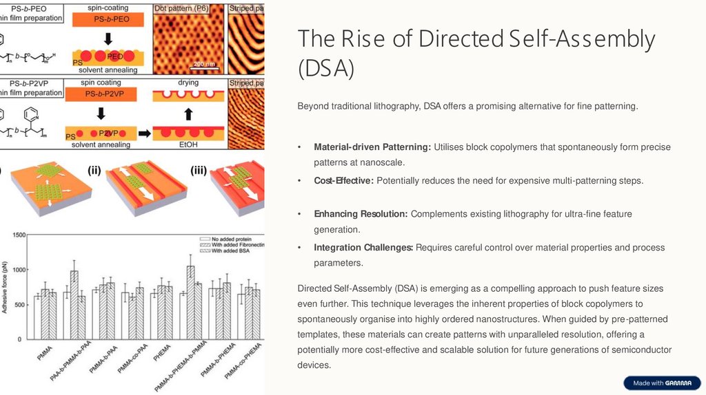
The Rise of Directed Self-Assembly(DSA)
Beyond traditional lithography, DSA offers a promising alternative for fine patterning.
Material-driven Patterning: Utilises block copolymers that spontaneously form precise
patterns at nanoscale.
Cost-Effective: Potentially reduces the need for expensive multi-patterning steps.
Enhancing Resolution: Complements existing lithography for ultra-fine feature
generation.
Integration Challenges: Requires careful control over material properties and process
parameters.
Directed Self-Assembly (DSA) is emerging as a compelling approach to push feature sizes
even further. This technique leverages the inherent properties of block copolymers to
spontaneously organise into highly ordered nanostructures. When guided by pre-patterned
templates, these materials can create patterns with unparalleled resolution, offering a
potentially more cost-effective and scalable solution for future generations of semiconductor
devices.
8.
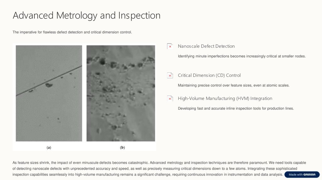
Advanced Metrology and InspectionThe imperative for flawless defect detection and critical dimension control.
Nanoscale Defect Detection
Identifying minute imperfections becomes increasingly critical at smaller nodes.
Critical Dimension (CD) Control
Maintaining precise control over feature sizes, even at atomic scales.
High-Volume Manufacturing (HVM) Integration
Developing fast and accurate inline inspection tools for production lines.
As feature sizes shrink, the impact of even minuscule defects becomes catastrophic. Advanced metrology and inspection techniques are therefore paramount. We need tools capable
of detecting nanoscale defects with unprecedented accuracy and speed, as well as precisely measuring critical dimensions down to a few atoms. Integrating these sophisticated
inspection capabilities seamlessly into high-volume manufacturing remains a significant challenge, requiring continuous innovation in instrumentation and data analysis.
9.
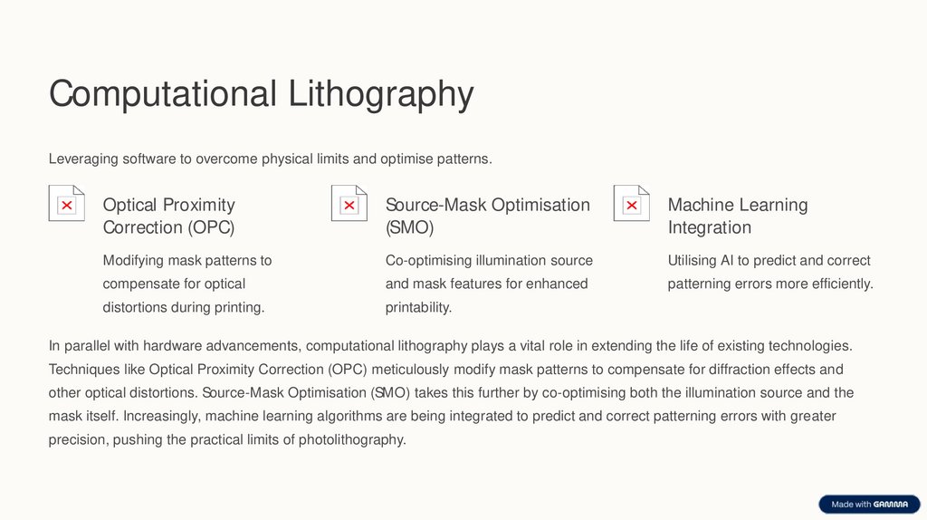
Computational LithographyLeveraging software to overcome physical limits and optimise patterns.
Optical Proximity
Correction (OPC)
Source-Mask Optimisation
(SMO)
Machine Learning
Integration
Modifying mask patterns to
Co-optimising illumination source
Utilising AI to predict and correct
compensate for optical
and mask features for enhanced
patterning errors more efficiently.
distortions during printing.
printability.
In parallel with hardware advancements, computational lithography plays a vital role in extending the life of existing technologies.
Techniques like Optical Proximity Correction (OPC) meticulously modify mask patterns to compensate for diffraction effects and
other optical distortions. Source-Mask Optimisation (SMO) takes this further by co-optimising both the illumination source and the
mask itself. Increasingly, machine learning algorithms are being integrated to predict and correct patterning errors with greater
precision, pushing the practical limits of photolithography.
10.
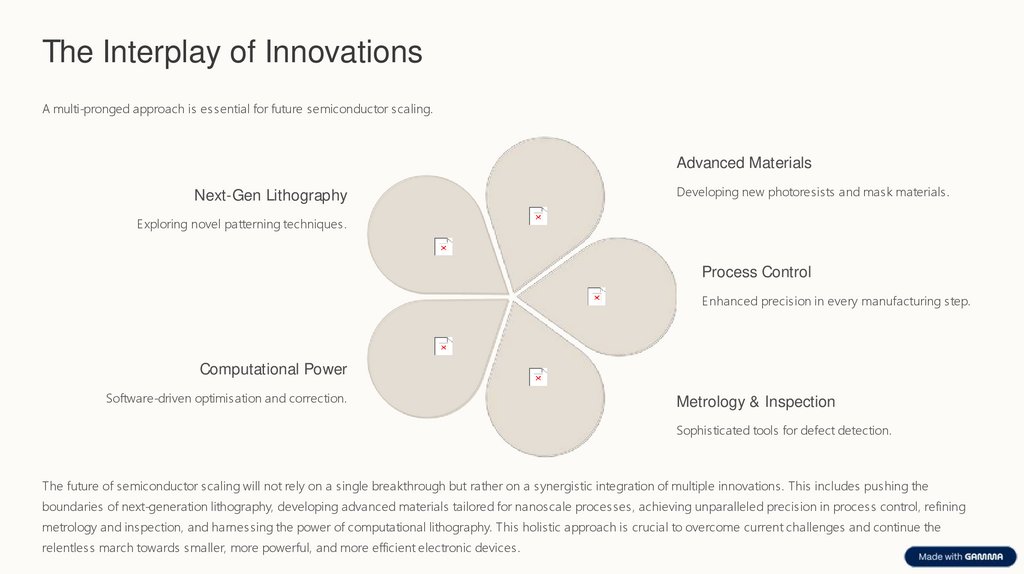
The Interplay of InnovationsA multi-pronged approach is essential for future semiconductor scaling.
Advanced Materials
Next-Gen Lithography
Developing new photoresists and mask materials.
E xploring novel patterning techniques.
Process Control
E nhanced precision in every manufacturing step.
Computational Power
Software-driven optimisation and correction.
Metrology & Inspection
Sophisticated tools for defect detection.
The future of semiconductor scaling will not rely on a single breakthrough but rather on a synergistic integration of multiple innovations. This includes pushing the
boundaries of next-generation lithography, developing advanced materials tailored for nanoscale processes, achieving unparalleled precision in process control, refining
metrology and inspection, and harnessing the power of computational lithography. This holistic approach is crucial to overcome current challenges and continue the
relentless march towards smaller, more powerful, and more efficient electronic devices.