


 electronics
Similar presentations:


D106 Platform. Schematic diagram Introduction
1.
D106 PlatformSchematic diagram Introduction
2.
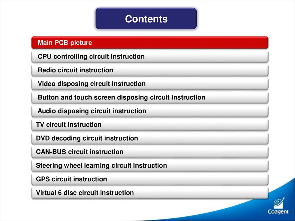
ContentsMain PCB picture
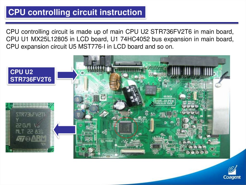
CPU controlling circuit instruction
Radio circuit instruction
Video disposing circuit instruction
Button and touch screen disposing circuit instruction
Audio disposing circuit instruction
TV circuit instruction
DVD decoding circuit instruction
CAN-BUS circuit instruction
Steering wheel learning circuit instruction
GPS circuit instruction
Virtual 6 disc circuit instruction
3.
ContentsMain PCB picture
CPU controlling circuit instruction
Radio circuit instruction
Video disposing circuit instruction
Button and touch screen disposing circuit instruction
Audio disposing circuit instruction
TV circuit instruction
DVD decoding circuit instruction
CAN-BUS circuit instruction
Steering wheel learning circuit instruction
GPS circuit instruction
Virtual 6 disc circuit instruction
4.
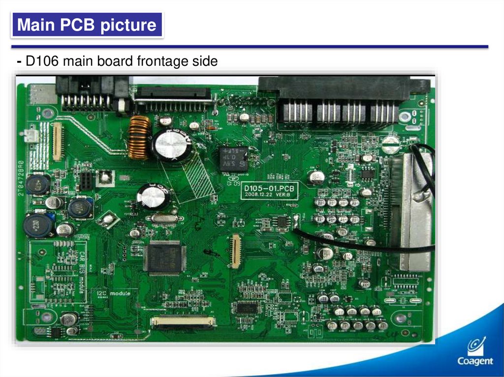
Main PCB picture- D106 main board frontage side
5.
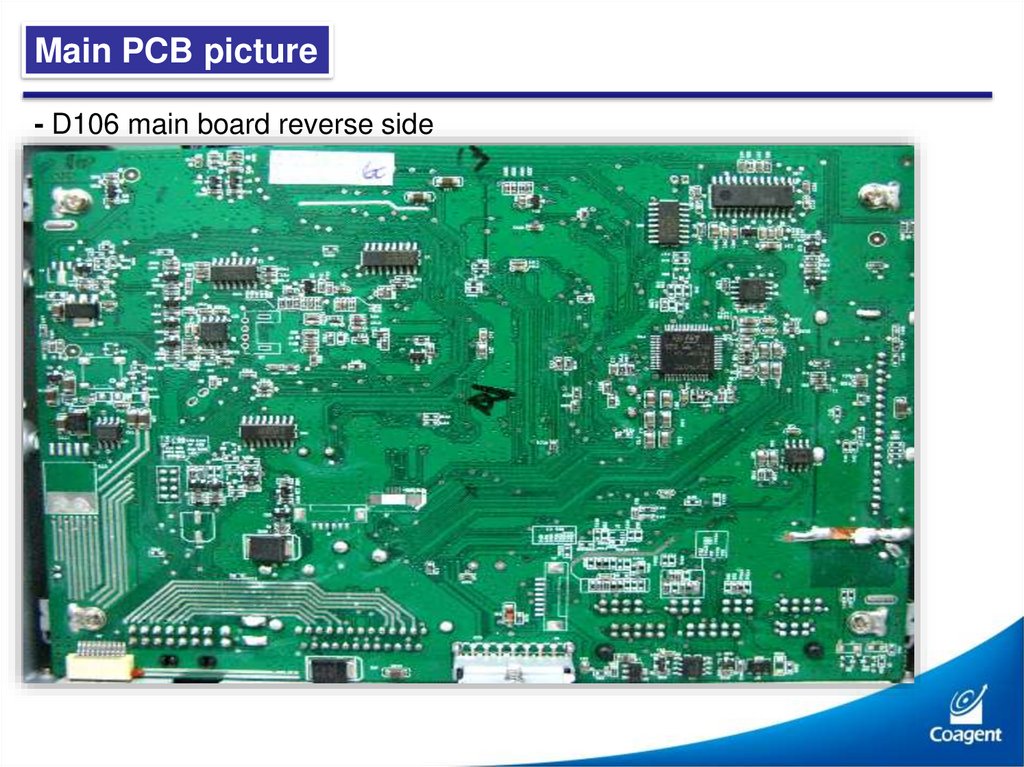
Main PCB picture- D106 main board reverse side
6.
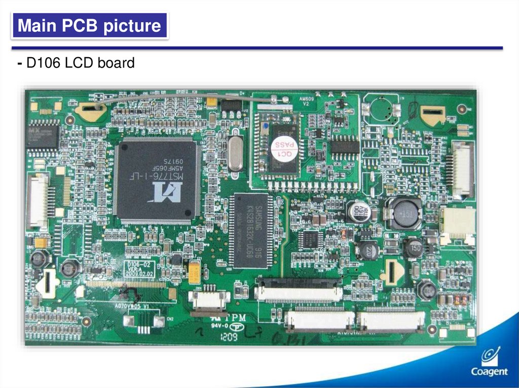
Main PCB picture- D106 LCD board
7.
ContentsMain PCB picture
CPU controlling circuit instruction
Radio circuit instruction
Video disposing circuit instruction
Button and touch screen disposing circuit instruction
Audio disposing circuit instruction
TV circuit instruction
DVD decoding circuit instruction
CAN-BUS circuit instruction
Steering wheel learning circuit instruction
GPS circuit instruction
Virtual 6 disc circuit instruction
8.
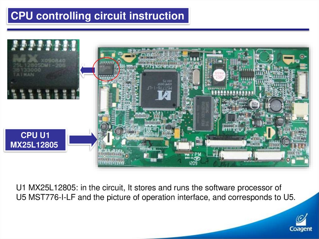
CPU controlling circuit instructionCPU controlling circuit is made up of main CPU U2 STR736FV2T6 in main board,
CPU U1 MX25L12805 in LCD board, U1 74HC4052 bus expansion in main board,
CPU expansion circuit U5 MST776-I in LCD board and so on.
CPU U2
STR736FV2T6
9.
CPU controlling circuit instructionU2 STR736FV2T6 in the circuit, mainly used for exchanging
function and controlling power converter
10.
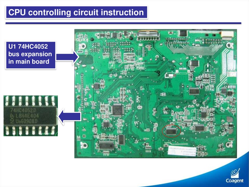
CPU controlling circuit instructionU1 74HC4052
bus expansion
in main board
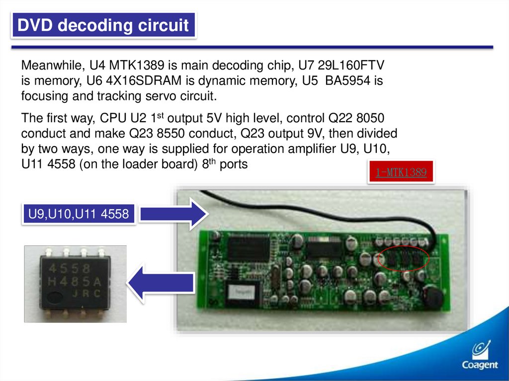
11.
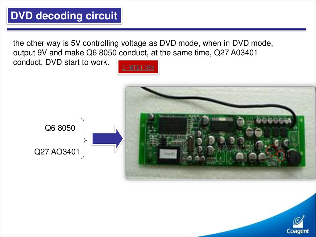
CPU controlling circuit instructionCPU U1
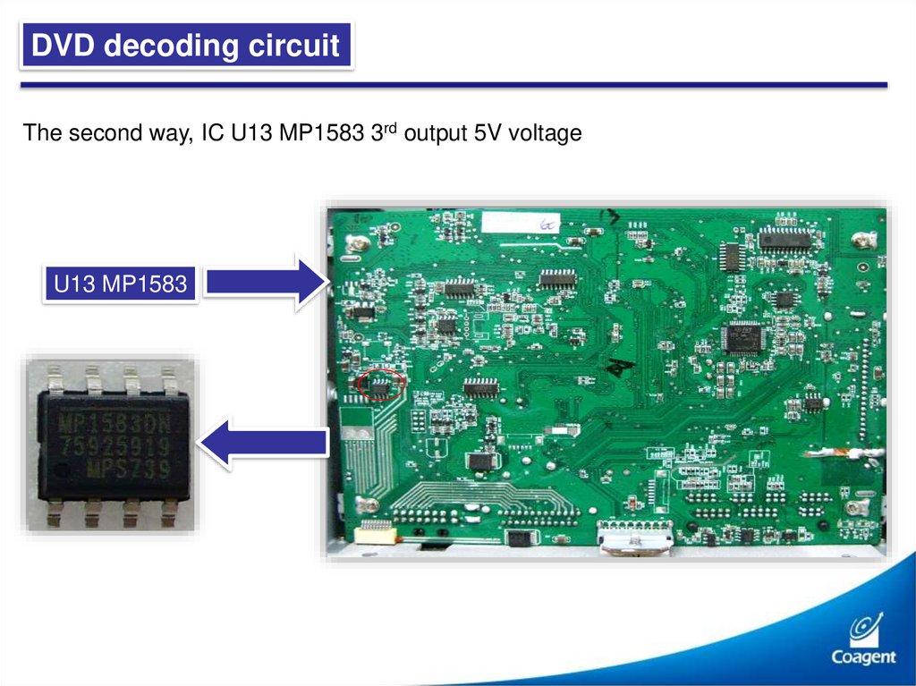
MX25L12805
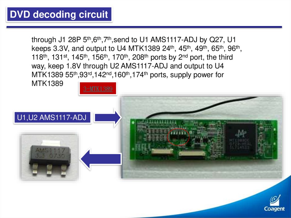
U1 MX25L12805: in the circuit, It stores and runs the software processor of
U5 MST776-I-LF and the picture of operation interface, and corresponds to U5.
12.
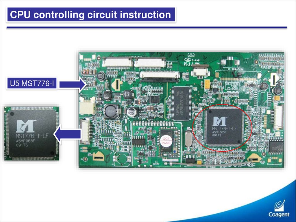
CPU controlling circuit instructionU5 MST776-I
13.
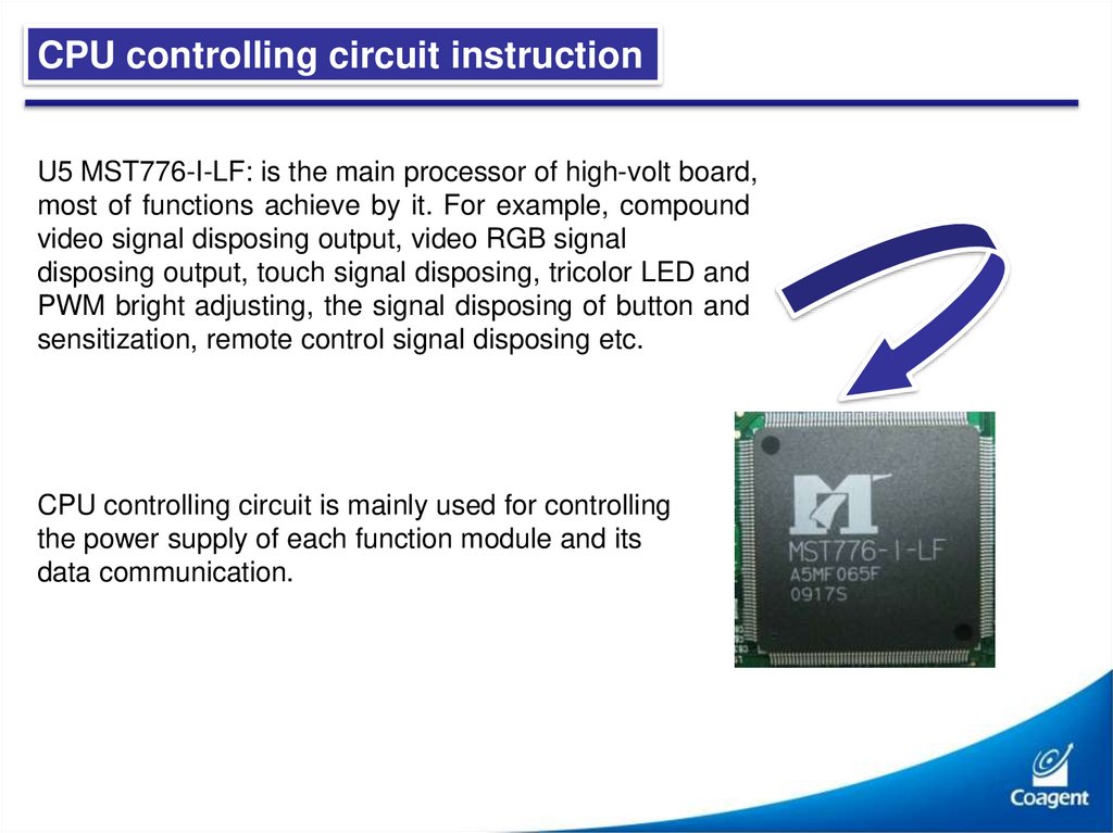
CPU controlling circuit instructionU5 MST776-I-LF: is the main processor of high-volt board,
most of functions achieve by it. For example, compound
video signal disposing output, video RGB signal
disposing output, touch signal disposing, tricolor LED and
PWM bright adjusting, the signal disposing of button and
sensitization, remote control signal disposing etc.
CPU controlling circuit is mainly used for controlling
the power supply of each function module and its
data communication.
14.
CPU controlling circuit instructionMeanwhile, the 5V voltage of U2
STR736FV2T6 8th, 36th, 48th, 63rd,
71st, 90th are supplied by BATT
multiple IC U23 HA13164A, then,
output 5V voltage from U23 4th
port, U23 HA13164A is a intensive
multiple voltage regulator
1-CPU
U23 HA13164A
15.
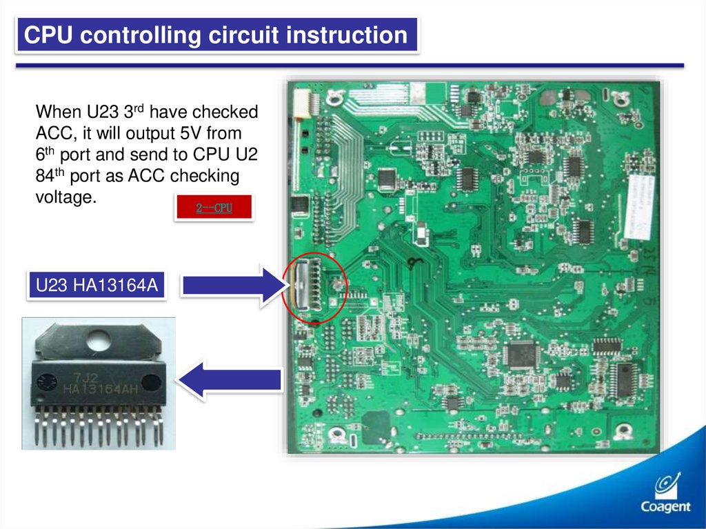
CPU controlling circuit instructionWhen U23 3rd have checked
ACC, it will output 5V from
6th port and send to CPU U2
84th port as ACC checking
voltage.
2--CPU
U23 HA13164A
16.
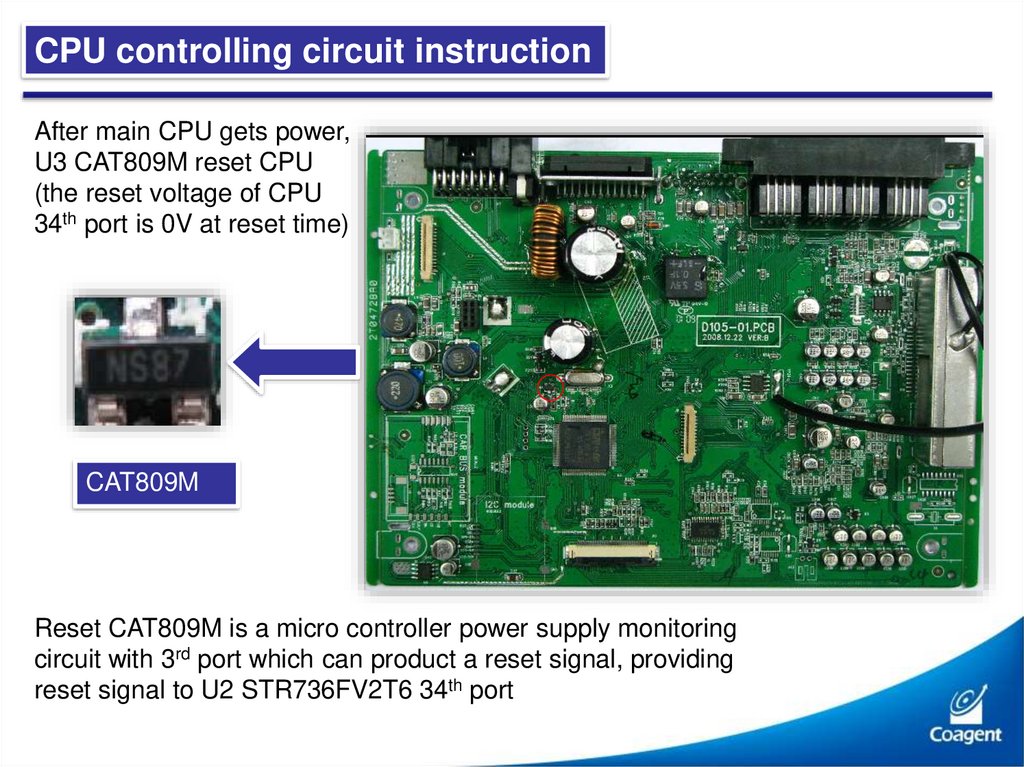
CPU controlling circuit instructionAfter main CPU gets power,
U3 CAT809M reset CPU
(the reset voltage of CPU
34th port is 0V at reset time)
CAT809M
Reset CAT809M is a micro controller power supply monitoring
circuit with 3rd port which can product a reset signal, providing
reset signal to U2 STR736FV2T6 34th port
17.
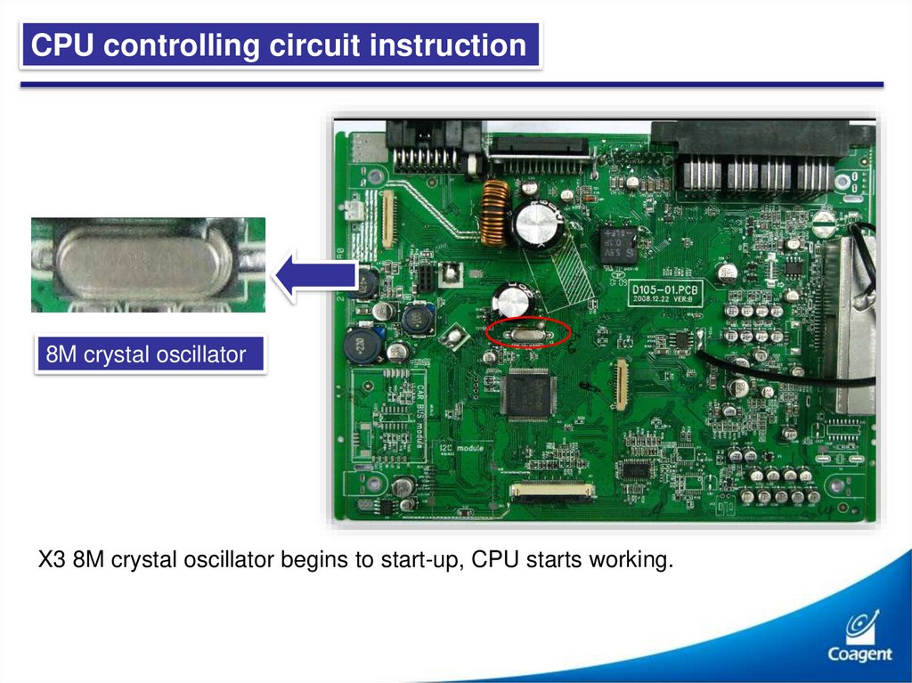
CPU controlling circuit instruction8M crystal oscillator
X3 8M crystal oscillator begins to start-up, CPU starts working.
18.
CPU controlling circuit instructionU2 is mainly controls DVD function circuit, RADIO function circuit,
CDC function circuit, GPS function circuit, TV function circuit,
Power amplifier control, lamp control, steering wheel control, RDS
data disposing and FAN control etc.
Meanwhile, the exchange of CDC and TV data is depended on CPU
91st and 94th ports controlling U1 74HC4052.
3--CPU
19.
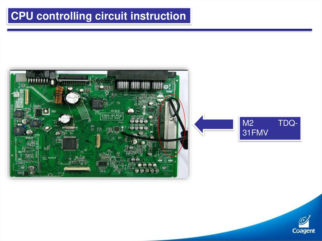
CPU controlling circuit instructionAnd CPU control U60 TDA7415, M2 TDQ-31FMV, U12 FMS6502,
and U52 24C02 by I2C bus (SCL, SDA).
U60 TDA7415
20.
CPU controlling circuit instructionM2
31FMV
TDQ-
21.
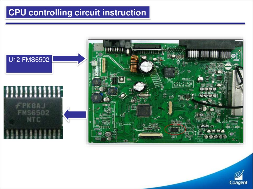
CPU controlling circuit instructionU12 FMS6502
22.
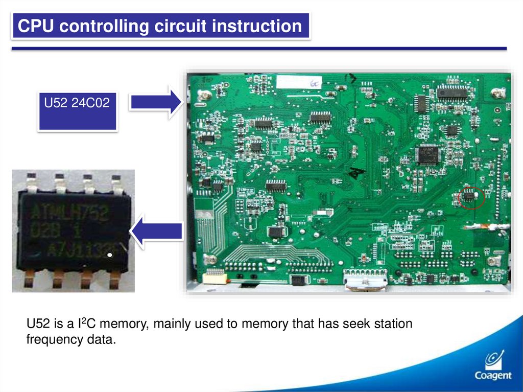
CPU controlling circuit instructionU52 24C02
U52 is a I2C memory, mainly used to memory that has seek station
frequency data.
23.
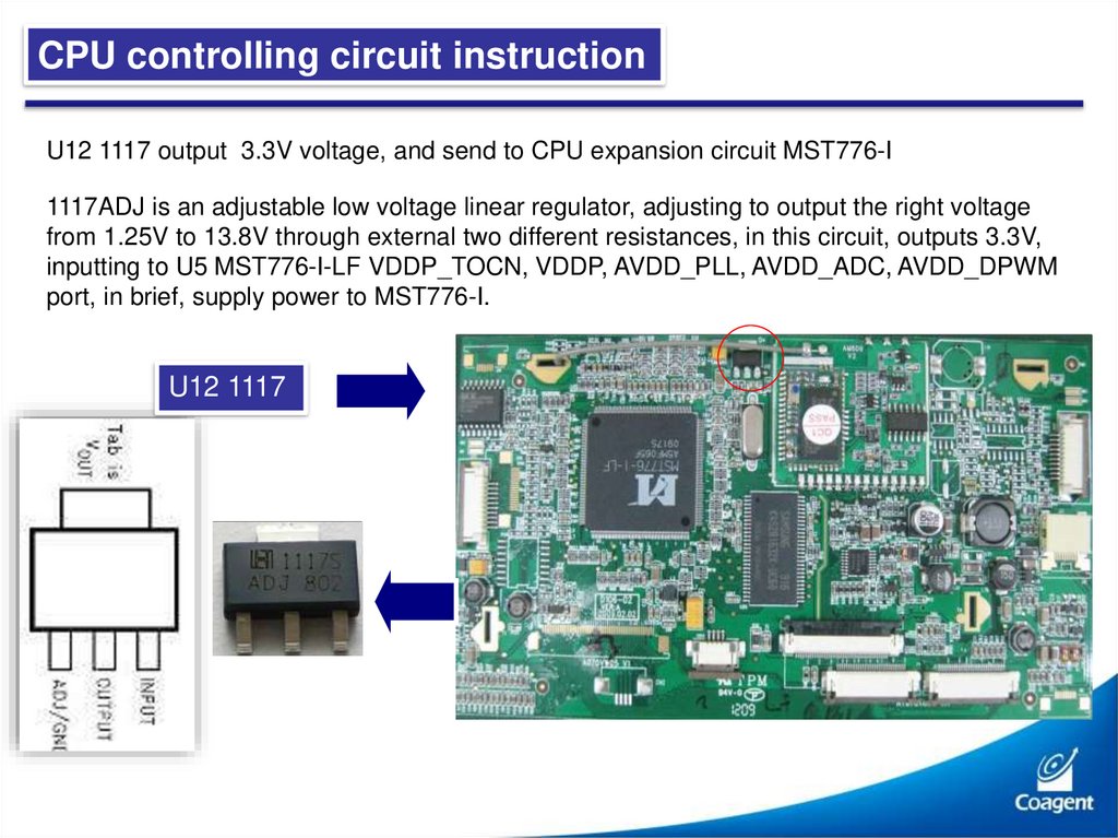
CPU controlling circuit instructionU12 1117 output 3.3V voltage, and send to CPU expansion circuit MST776-I
1117ADJ is an adjustable low voltage linear regulator, adjusting to output the right voltage
from 1.25V to 13.8V through external two different resistances, in this circuit, outputs 3.3V,
inputting to U5 MST776-I-LF VDDP_TOCN, VDDP, AVDD_PLL, AVDD_ADC, AVDD_DPWM
port, in brief, supply power to MST776-I.
U12 1117
24.
CPU controlling circuit instructionAnd U3 AO3401 output 1.8V voltage and send to CPU expansion circuit MST776-I
AO3401 and external elements are made up of a DC-DC reducing voltage circuit,
providing 1.8V for MST776-I ADC (analog and digital converter) circuit.
U3 AO3401
25.
CPU controlling circuit instructionMain CPU U2 23rd port is MUTE control (Note: the voltage of this port is
always 5V when pressing MUTE button, CPU U2 43rd and 44th control
U60 TDA7415, in order to achieve MUTE function finally), 34th is reset
port, 84th is ACC detecting port, 38th and 39th are crystal oscillator ports,
7th is HANDBRAKE signal input port, 10th is BACK signal input port, 1st
is DVD mode power control, 13th is CDC mode control, 58th is RADIO
mode power supply control.
4--CPU
26.
CPU controlling circuit instructionCPU circuit basic power supply
5V power supply U2 STR736FV2T6 8th, 36th, 48th, 63rd, 71st, 90th, power
supply from IC U23 HA13164A 4th port
ACC monitoring voltage is 5V when open ACC, U23 3rd detect ACC, output
5V from 6th port, communicate to U2 84th port as detecting voltage
MST776-I 3.3V output from U12 1117 (is in LCD board)
MST776-I 1.8V output from U3 AO3401
27.
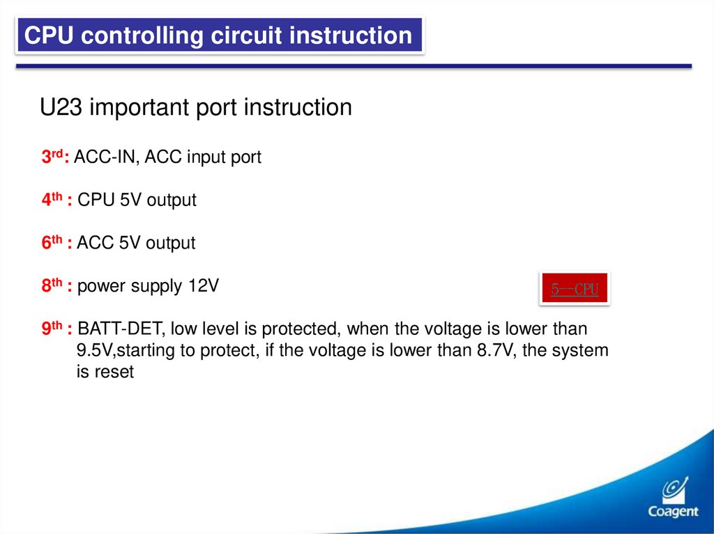
CPU controlling circuit instructionU23 important port instruction
3rd: ACC-IN, ACC input port
4th : CPU 5V output
6th : ACC 5V output
8th : power supply 12V
5--CPU
9th : BATT-DET, low level is protected, when the voltage is lower than
9.5V,starting to protect, if the voltage is lower than 8.7V, the system
is reset
28.
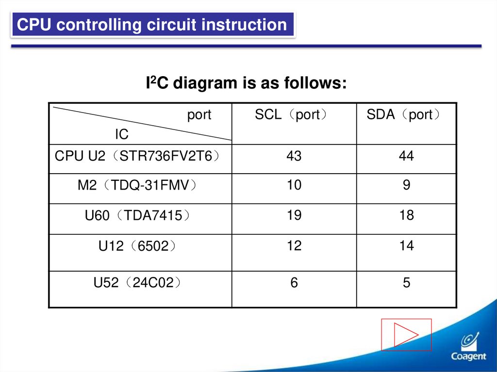
CPU controlling circuit instructionI2C diagram is as follows:
port
SCL port
SDA port
CPU U2 STR736FV2T6
43
44
M2 TDQ-31FMV
10
9
U60 TDA7415
19
18
U12 6502
12
14
U52 24C02
6
5
IC
29.
ContentsMain PCB picture
CPU controlling circuit instruction
Radio circuit instruction
Video disposing circuit instruction
Button and touch screen disposing circuit instruction
Audio disposing circuit instruction
TV circuit instruction
DVD decoding circuit instruction
CAN-BUS circuit instruction
Steering wheel learning circuit instruction
GPS circuit instruction
Virtual 6 disc circuit instruction
30.
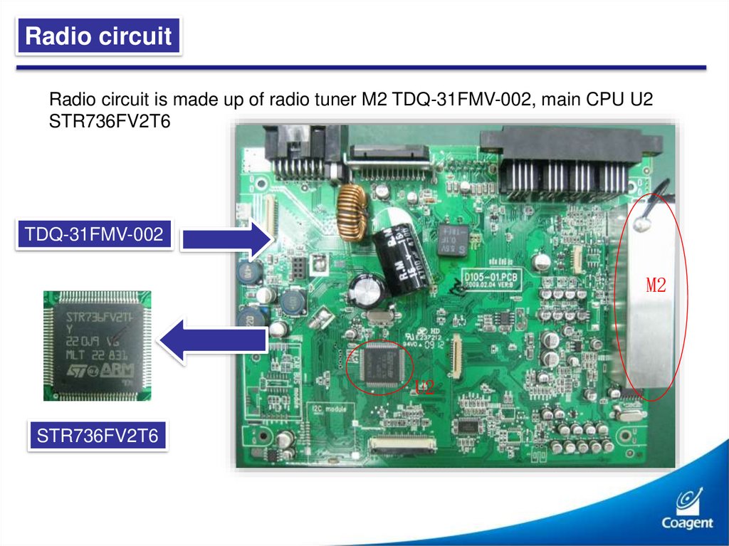
Radio circuitRadio circuit is made up of radio tuner M2 TDQ-31FMV-002, main CPU U2
STR736FV2T6
TDQ-31FMV-002
M2
U2
STR736FV2T6
31.
Radio circuitRDS function disposing IC U116 BU1924F and X1 4.332M crystal oscillator.
U116 BU1924F is a RDS (Radio
Data System, Europe standard)
/RBDS (Radio Broadcast Data
System North America standard)
demodulator.
BU1924F
4.332M
32.
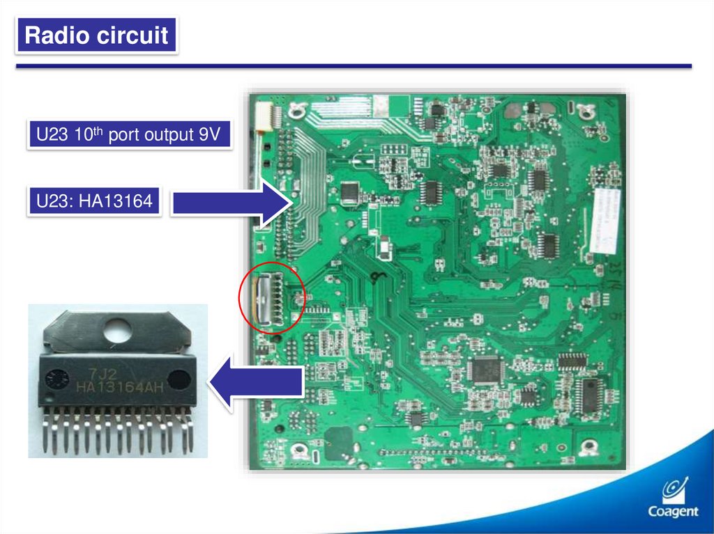
Radio circuitU23 10th port output 9V
U23: HA13164
33.
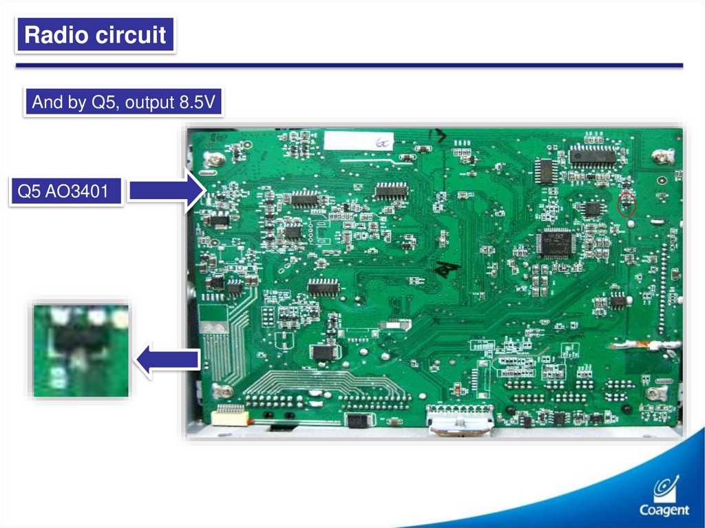
Radio circuitAnd by Q5, output 8.5V
Q5 AO3401
34.
Radio circuitThen send to tuner 19th port (Note: when in radio mode, main CPU U2 58th
port output 5V and make Q13 8050 conducted, Q5 is also conducted), the 5V
of tuner 11th port is provided by U23 HA13164 5th port, then radio circuit starts
to work. Tuner 8th, 9th, 10th, 14th ports and main CPU U2 12th, 43rd, 44th, 57th
ports finish seeking, saving stations. (the voltage of tuner 8th port SSTOP is
about 0.14V when in the mode of seeking, the instant voltage is 5.2V when in
mode of saving. The voltage of tuner 14th port QUALY is 5V when in the mode
of seeking, the instant voltage is 1.9V when in the mode of saving. The voltage
is 1.9V when in the mode of playing radio station. The voltage of tuner bus
ports 9th SDA and 10th SCL are about 5.2V)
1--Radio
35.
Radio circuit - RDS circuitThe Left/Right audio signals which decoded by tuner, through tuner 16th and
17th ports, output to U60 TDA7415 59th and 60th ports, then amplified by
amplifier (note: the voltage of 16th and 17th ports are about 3V)
2--Radio
RDS function is made by U116 BU1924F 2nd and 16th ports, through CPU U2
25th RDS DATA and 62nd RDS CLK, control U116 4th port and output controlling
signal to tuner 12th port, in order to achieve RDS function
3--Radio
36.
ContentsMain PCB picture
CPU controlling circuit instruction
Radio circuit instruction
Video disposing circuit instruction
Button and touch screen disposing circuit instruction
Audio disposing circuit instruction
TV circuit instruction
DVD decoding circuit instruction
CAN-BUS circuit instruction
Steering wheel learning circuit instruction
GPS circuit instruction
Virtual 6 disc circuit instruction
37.
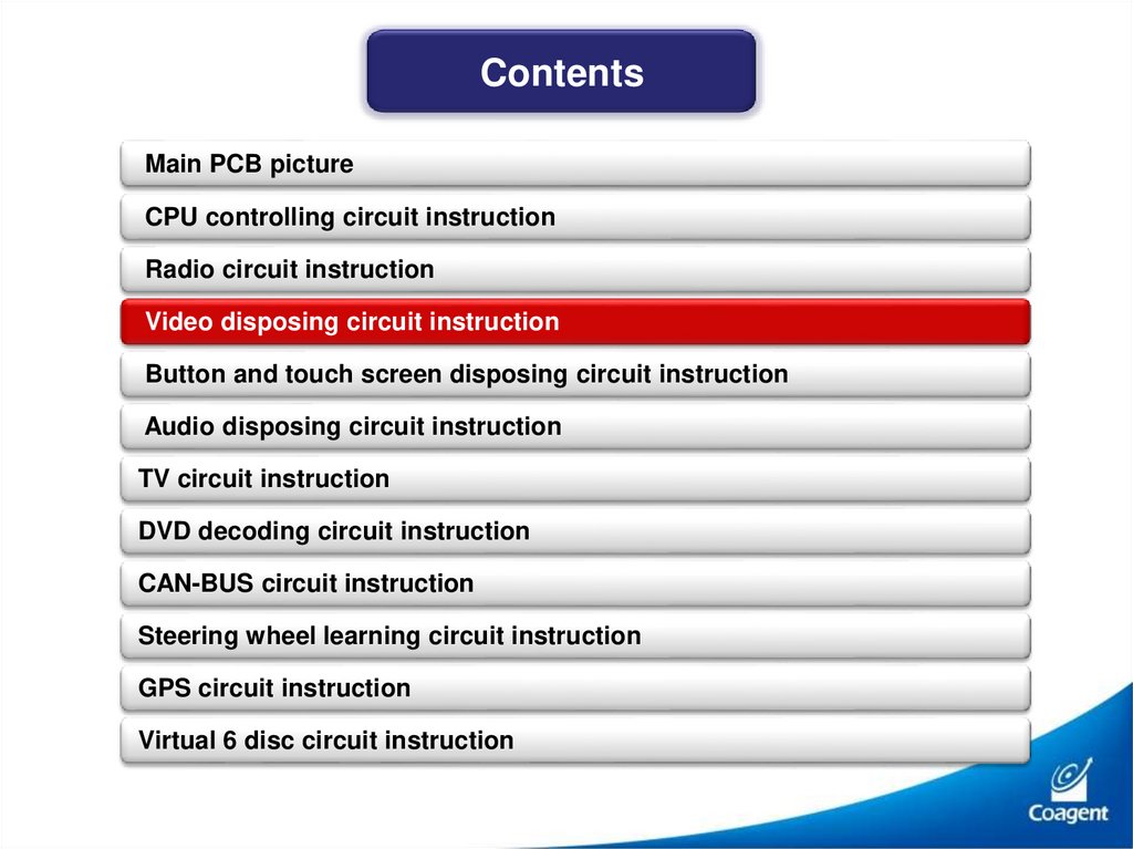
Video disposing circuitVideo disposing is made up of U5 MST776-I, and U12 FMS6502 electronic
switch etc
U5 MST776-I
38.
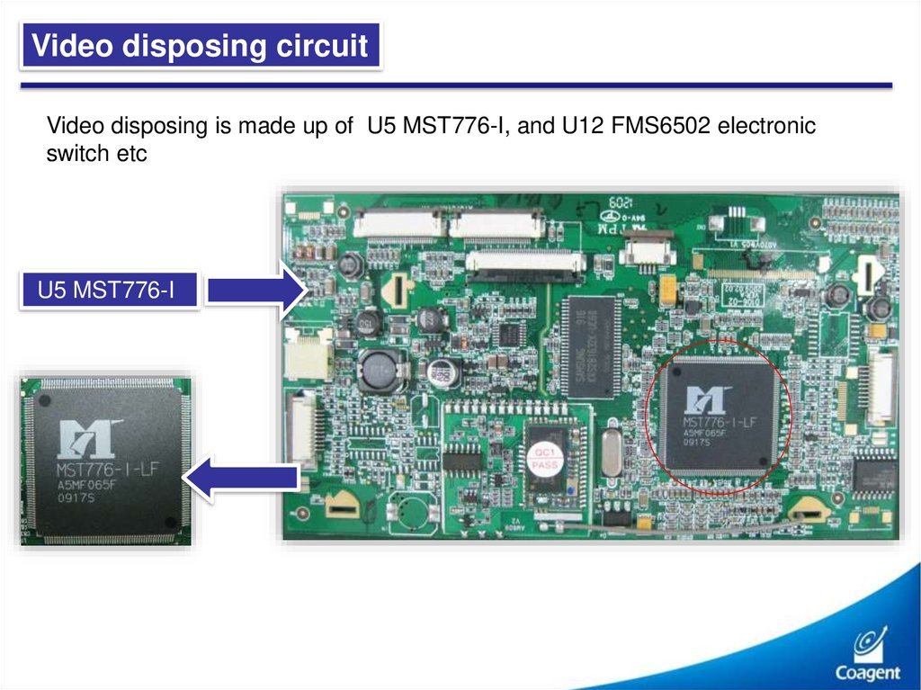
Video disposing circuitU12 FMS6502
39.
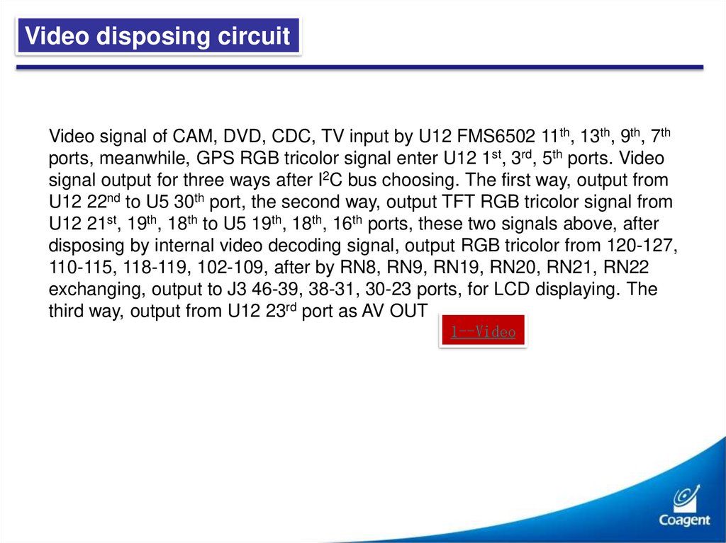
Video disposing circuitVideo signal of CAM, DVD, CDC, TV input by U12 FMS6502 11th, 13th, 9th, 7th
ports, meanwhile, GPS RGB tricolor signal enter U12 1st, 3rd, 5th ports. Video
signal output for three ways after I2C bus choosing. The first way, output from
U12 22nd to U5 30th port, the second way, output TFT RGB tricolor signal from
U12 21st, 19th, 18th to U5 19th, 18th, 16th ports, these two signals above, after
disposing by internal video decoding signal, output RGB tricolor from 120-127,
110-115, 118-119, 102-109, after by RN8, RN9, RN19, RN20, RN21, RN22
exchanging, output to J3 46-39, 38-31, 30-23 ports, for LCD displaying. The
third way, output from U12 23rd port as AV OUT
1--Video
40.
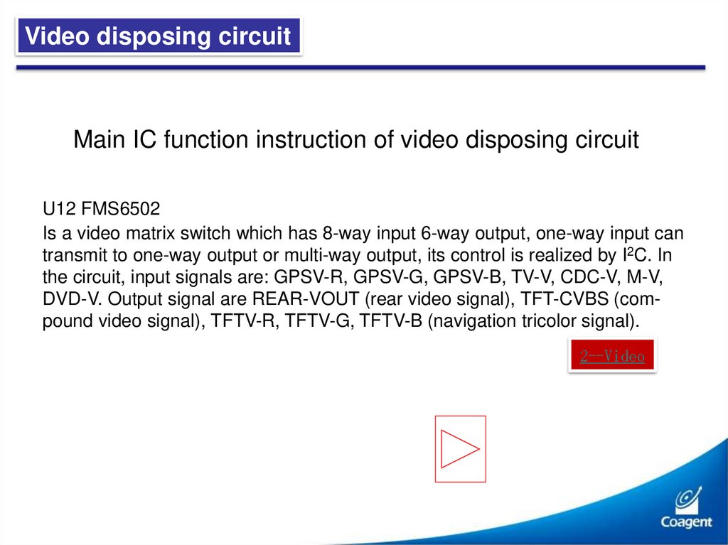
Video disposing circuitMain IC function instruction of video disposing circuit
U12 FMS6502
Is a video matrix switch which has 8-way input 6-way output, one-way input can
transmit to one-way output or multi-way output, its control is realized by I2C. In
the circuit, input signals are: GPSV-R, GPSV-G, GPSV-B, TV-V, CDC-V, M-V,
DVD-V. Output signal are REAR-VOUT (rear video signal), TFT-CVBS (compound video signal), TFTV-R, TFTV-G, TFTV-B (navigation tricolor signal).
2--Video
41.
ContentsMain PCB picture
CPU controlling circuit instruction
Radio circuit instruction
Video disposing circuit instruction
Button and touch screen disposing circuit instruction
Audio disposing circuit instruction
TV circuit instruction
DVD decoding circuit instruction
CAN-BUS circuit instruction
Steering wheel learning circuit instruction
GPS circuit instruction
Virtual 6 disc circuit instruction
42.
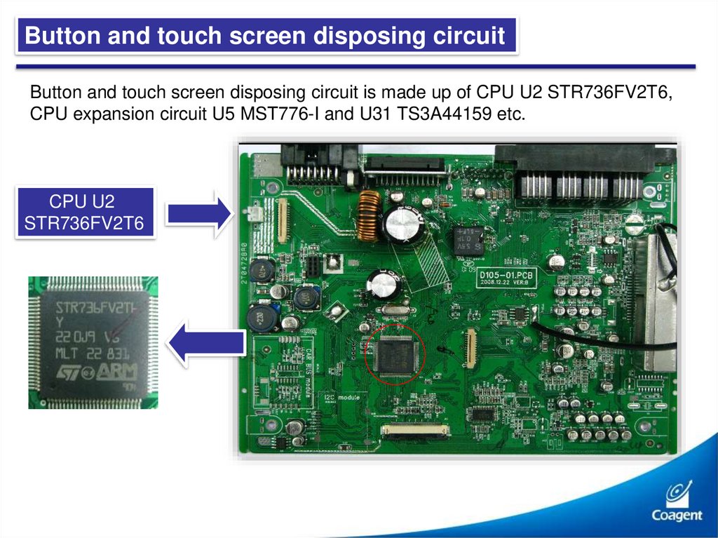
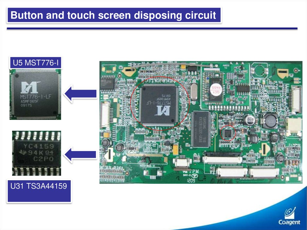
Button and touch screen disposing circuitButton and touch screen disposing circuit is made up of CPU U2 STR736FV2T6,
CPU expansion circuit U5 MST776-I and U31 TS3A44159 etc.
CPU U2
STR736FV2T6
43.
Button and touch screen disposing circuitU5 MST776-I
U31 TS3A44159
44.
Button and touch screen disposing circuitButton disposing enters U5 MST776-I 66th,64th ports by button matrix circuit
. X1 axis, Y1 axis, X2 axis, Y2 axis on the touch screen were match to D34,
D35, D36, D37(BAT54S), they make up of touch screen matrix circuit, they
become matrix voltage and send to U31 TS3A44159 7th, 11th, 15th, 3rd ports.
GPS touch handwriting signal enter U31 1st, 13th, 9th, 5th port. (Note:U31
TS3A44159 8th is switch port from navigation mode to other function mode,
the voltage of this port is 0V when in mode of navigation, and the voltage of
this port is 5V when in the other function mode), these two signals above,
output to CPU U2 STR736FV2T6 77th,78th,19th,76th,82nd ports by
TS3A44159 electronic switch internal exchanging, in order to finish some
signal communications such as clock, chip-select, enable, data and interrupt
1--Button
45.
Button and touch screen disposing circuitU31 TS3A44159 12th is power port, the voltage which is from U13 MP1583
3rd 5V. When U5 MST776-I-LF 88th port input high/low level to TS3A44159
IN1-2, IN3-4 GPS_T_SW, may achieve touch signal converter.
2--Button
U13 MP1583
46.
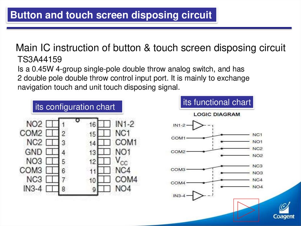
Button and touch screen disposing circuitMain IC instruction of button & touch screen disposing circuit
TS3A44159
Is a 0.45W 4-group single-pole double throw analog switch, and has
2 double pole double throw control input port. It is mainly to exchange
navigation touch and unit touch disposing signal.
its configuration chart
its functional chart
47.
ContentsMain PCB picture
CPU controlling circuit instruction
Radio circuit instruction
Video disposing circuit instruction
Button and touch screen disposing circuit instruction
Audio disposing circuit instruction
TV circuit instruction
DVD decoding circuit instruction
CAN-BUS circuit instruction
Steering wheel learning circuit instruction
GPS circuit instruction
Virtual 6 disc circuit instruction
48.
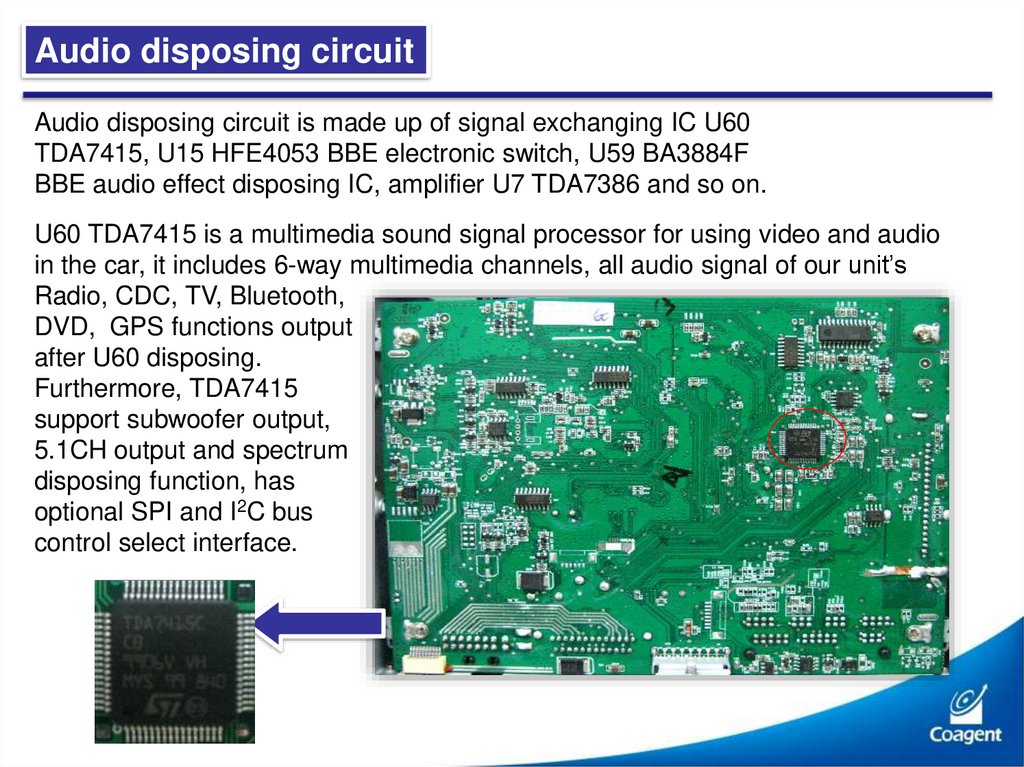
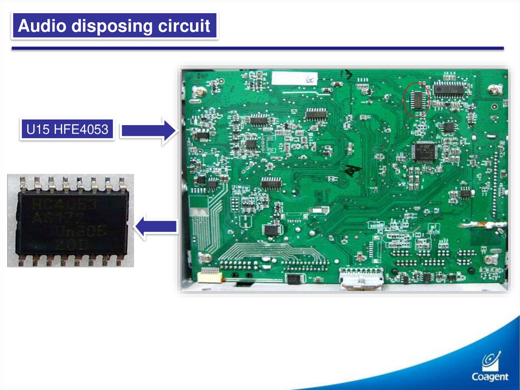
Audio disposing circuitAudio disposing circuit is made up of signal exchanging IC U60
TDA7415, U15 HFE4053 BBE electronic switch, U59 BA3884F
BBE audio effect disposing IC, amplifier U7 TDA7386 and so on.
U60 TDA7415 is a multimedia sound signal processor for using video and audio
in the car, it includes 6-way multimedia channels, all audio signal of our unit’s
Radio, CDC, TV, Bluetooth,
DVD, GPS functions output
after U60 disposing.
Furthermore, TDA7415
support subwoofer output,
5.1CH output and spectrum
disposing function, has
optional SPI and I2C bus
control select interface.
49.
Audio disposing circuitU15 HFE4053
50.
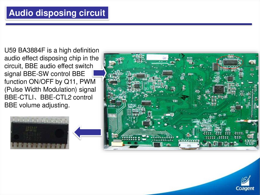
Audio disposing circuitU59 BA3884F is a high definition
audio effect disposing chip in the
circuit, BBE audio effect switch
signal BBE-SW control BBE
function ON/OFF by Q11, PWM
(Pulse Width Modulation) signal
BBE-CTLI、BBE-CTL2 control
BBE volume adjusting.
51.
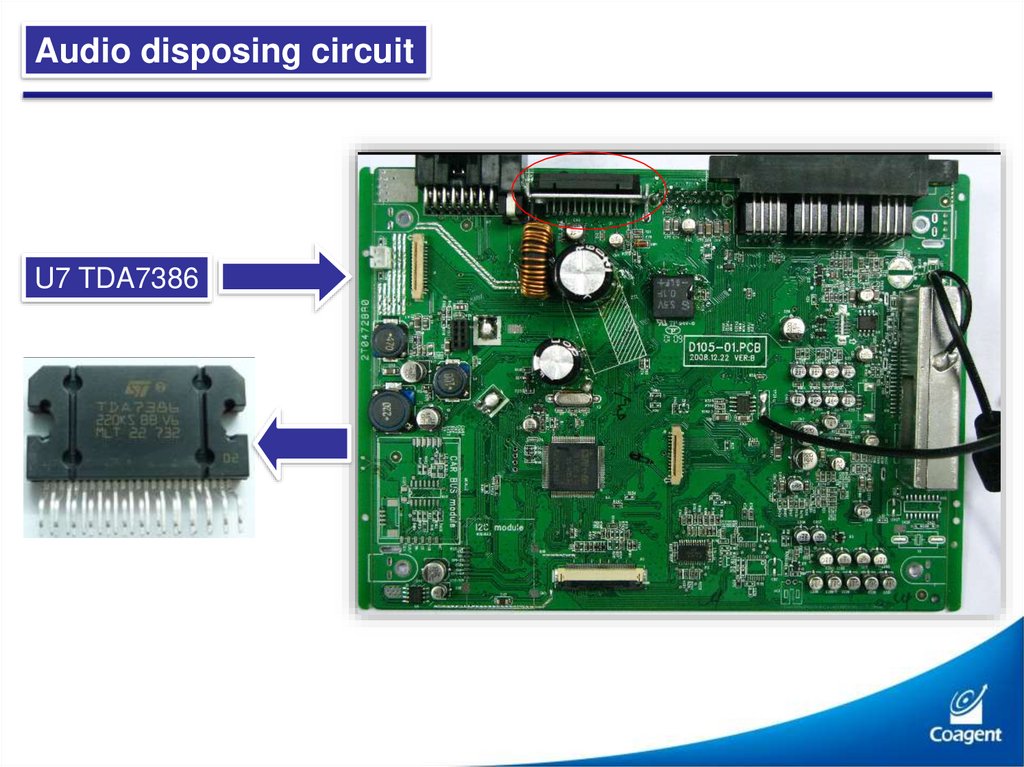
Audio disposing circuitU7 TDA7386
52.
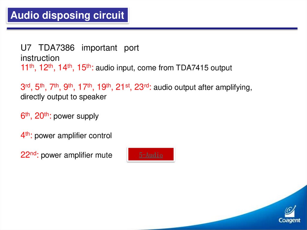
Audio disposing circuitU7 TDA7386 important port
instruction
11th, 12th, 14th, 15th: audio input, come from TDA7415 output
3rd, 5th, 7th, 9th, 17th, 19th, 21st, 23rd: audio output after amplifying,
directly output to speaker
6th, 20th: power supply
4th: power amplifier control
22nd: power amplifier mute
5-Audio
53.
Audio disposing circuitThe inputting audio signal from AV, DVD, GPS, CDC, TV, PHONE, RADIO
modes output by 3 ways through U60 internal exchanging. The first way,
output Left/right audio signal from U60 7th and 8th ports, then divided by
two ways: one way, output to U15 HFE4053 3rd and 1st ports, when BBE
function has not opened, output Left/Right audio signal from U15 4th and
15th ports, and send to U60 25th and 26th ports, by internal disposing,
output 4 channels to IC U7 amplifier. The other way, send U59 23rd and
14th ports and finish BBE disposing,
meanwhile, main CPU 5th,31st,32nd control BBE switch and BBE gain
adjustment, when open BBE, CPU U2 5th port (BBE-SW) output high voltage 5V (Note: BBE function of this unit is default ON, the voltage of this
port is 5V), now the audio signal output from U59 24th,13th ports to U15 5th
and 2nd ports by BBE disposing, after U15 exchanging, output from U15th
and 15th ports to U60 25th and 26th ports.
1--AUDIO
54.
Audio disposing circuitThen output standard 4 channels from U60 52nd, 53rd, 54th, 55th ports
to IC U7 11th, 12th, 14th, 15th ports after internal amplifying, output and
promote original speaker.
2--AUDIO
The second way, output 5.1CH audio signal from 43rd, 44th, 45th, 46th,
49th, 50th ports, in order to external 5.1CH amplifier. 3--AUDIO
The third way, output Left/Right audio signal from 9th and 10th ports
as AV audio signal output. Main CPU 23rd output MUTE signal to IC
U7 22nd port (Note: the voltage of this port is always 5V, when
pressing the MUTE button, CPU control U60 TDA7415 by 43rd SCL,
44th SDA, in order to achieve MUTE function). Main CPU 24th port
output AMP–P controlling signal (start when the high voltage is 5V)
4--AUDIO
55.
ContentsMain PCB picture
CPU controlling circuit instruction
Radio circuit instruction
Video disposing circuit instruction
Button and touch screen disposing circuit instruction
Audio disposing circuit instruction
TV circuit instruction
DVD decoding circuit instruction
CAN-BUS circuit instruction
Steering wheel learning circuit instruction
GPS circuit instruction
Virtual 6 disc circuit instruction
56.
TV circuitTV circuit is made up of TV tuner, main CPU U2 STR736FV2T6, D103-05.
PCB board and so on.
In D103-05.PCB, J26 and J8 is used for external TV antenna, seeking signal
and store broadcasting station, all ports of J45 communicate with CPU and
TV tuner, J45 10th is 5V power supply port, TV start to work when U2 49th
port output high level, J45 8th is TV video port, 5th and 6th are TV Left/Right
audio ports, 6th Left audio port connect to U60 TDA7415 61st by resistance
R502, 5th Right audio port connect to U60 TDA7415 62nd by resistance R503,
Finish TV function audio circuit. CPU control TV circuit working by I2C, 2nd is
clock bus port (SCL), 3rd is data bus port (SDA).
1--TV
Note: in D106 platform, TV tuner use M16WTP-PN-E, if use D103 platform
9886 tuner, it can cause no audio in TV mode.
57.
TV circuitThe picture of TV tuner M16WTP-PN-E is as follows:
TV tuner frontage side
TV tuner reverse side
58.
ContentsMain PCB picture
CPU controlling circuit instruction
Radio circuit instruction
Video disposing circuit instruction
Button and touch screen disposing circuit instruction
Audio disposing circuit instruction
TV circuit instruction
DVD decoding circuit instruction
CAN-BUS circuit instruction
Steering wheel learning circuit instruction
GPS circuit instruction
Virtual 6 disc circuit instruction
59.
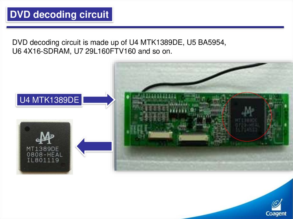
DVD decoding circuitDVD decoding circuit is made up of U4 MTK1389DE, U5 BA5954,
U6 4X16-SDRAM, U7 29L160FTV160 and so on.
U4 MTK1389DE
60.
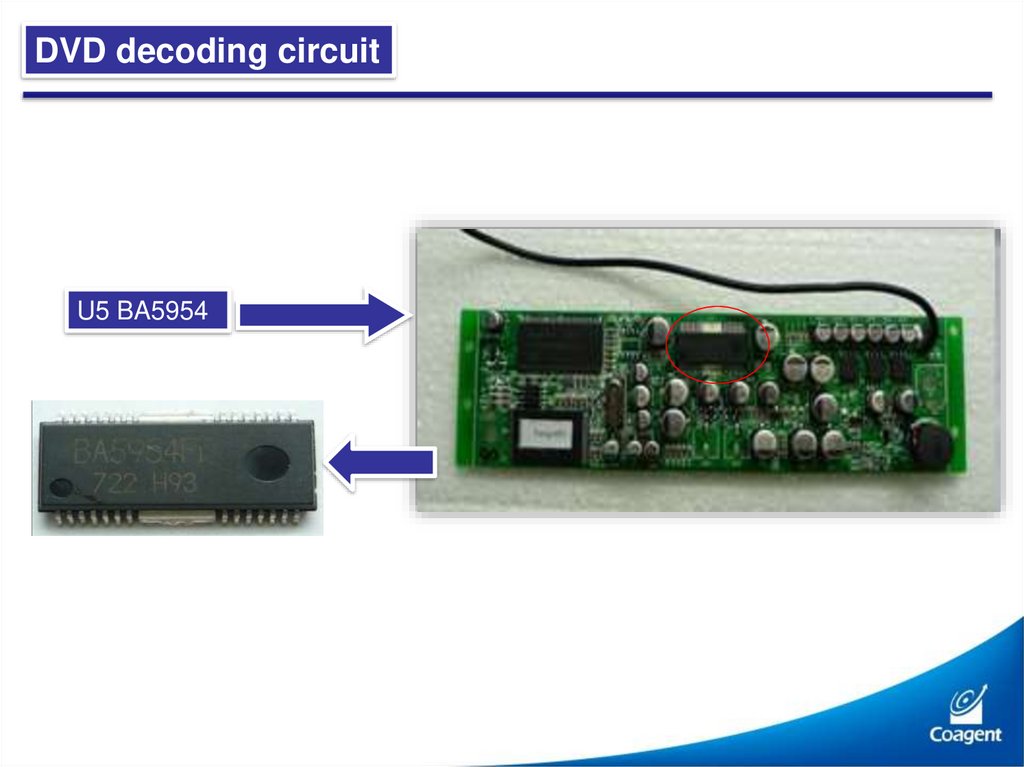
DVD decoding circuitU5 BA5954
61.
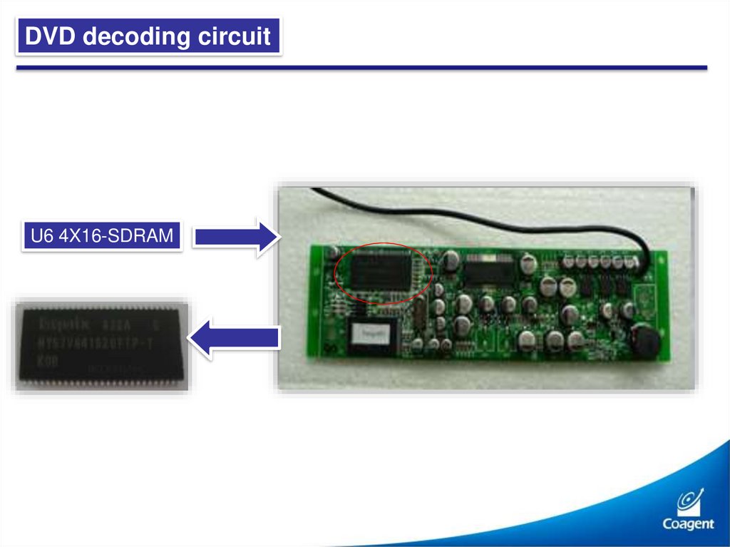
DVD decoding circuitU6 4X16-SDRAM
62.
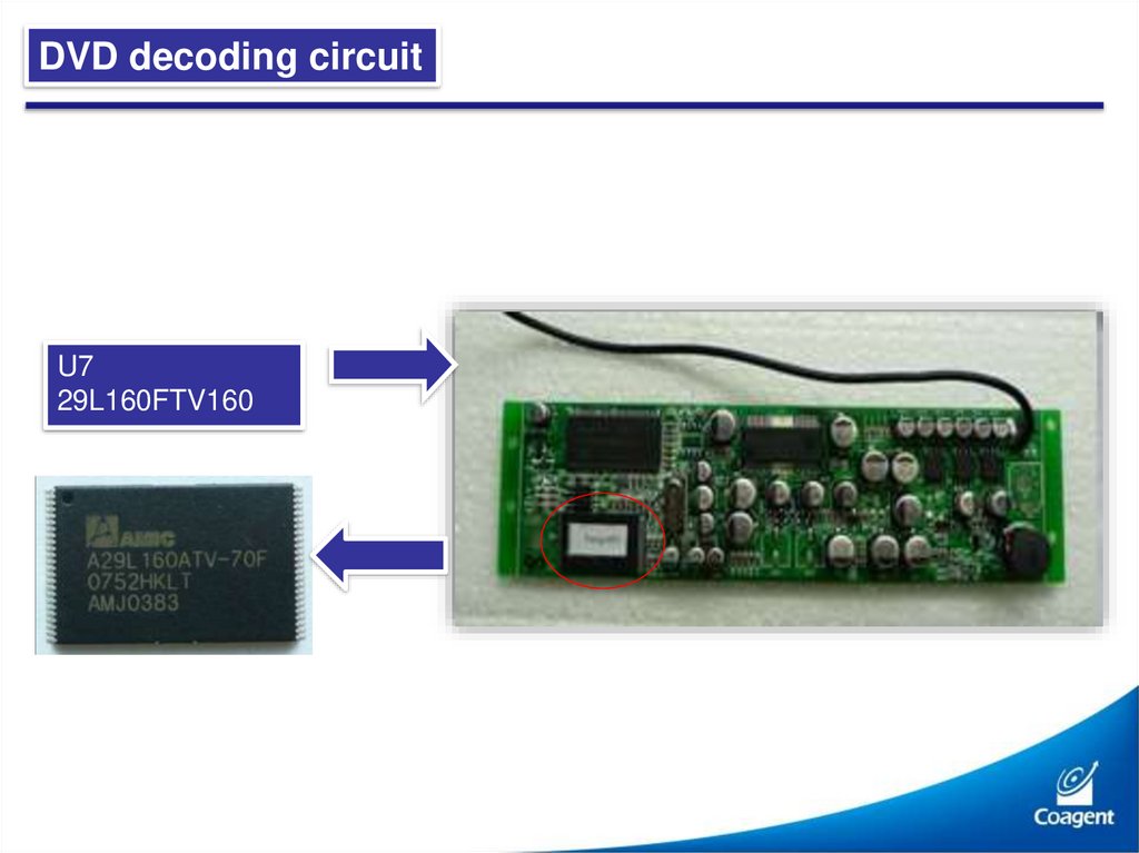
DVD decoding circuitU7
29L160FTV160
63.
DVD decoding circuitMeanwhile, U4 MTK1389 is main decoding chip, U7 29L160FTV
is memory, U6 4X16SDRAM is dynamic memory, U5 BA5954 is
focusing and tracking servo circuit.
The first way, CPU U2 1st output 5V high level, control Q22 8050
conduct and make Q23 8550 conduct, Q23 output 9V, then divided
by two ways, one way is supplied for operation amplifier U9, U10,
U11 4558 (on the loader board) 8th ports
1-MTK1389
U9,U10,U11 4558
64.
DVD decoding circuitthe other way is 5V controlling voltage as DVD mode, when in DVD mode,
output 9V and make Q6 8050 conduct, at the same time, Q27 A03401
conduct, DVD start to work.
2-MTK1389
Q6 8050
Q27 AO3401
65.
DVD decoding circuitThe second way, IC U13 MP1583 3rd output 5V voltage
U13 MP1583
66.
DVD decoding circuitthrough J1 28P 5th,6th,7th,send to U1 AMS1117-ADJ by Q27, U1
keeps 3.3V, and output to U4 MTK1389 24th, 45th, 49th, 65th, 96th,
118th, 131st, 145th, 156th, 170th, 208th ports by 2nd port, the third
way, keep 1.8V through U2 AMS1117-ADJ and output to U4
MTK1389 55th,93rd,142nd,160th,174th ports, supply power for
MTK1389
3-MTK1389
U1,U2 AMS1117-ADJ
67.
DVD decoding circuitThe external circuit of MTK1389 decoding chip, X1 27M crystal
oscillator connects U4 MTK1389 233rd and 234th ports, the
voltage of U8 24C04 8th port is 3.3V, 1st,2nd,3rd 4th ports are grounding,
5th is SDA, 6th is SCL.
U7 29L160FTV-70 is the memory for DVD starting interface message
memory chip. It is the memory of MTK1389, too. The voltages of
11th,14th and 37th ports are 3.3V. The voltage of 12th reset port is 3.3V.
4-MTK1389
68.
DVD decoding circuitU6 Flash memory 4X16-SDRAM supply data storage provisionally,
it will keep the data steady when electronic shockproof. The voltages
of that chip 1st, 3rd, 9th, 14th, 27th, 43rd and 49th ports are 3.3V. The 6th,
12th, 28th, 41st, 46th, 52nd and 54th ports are grounding. 5-MTK1389
DVD controlling signals like DATA, SCL, SDA, CS, CLK, LOAD-SW,
OPEN-SW and COLSE-SW enter MTK1389 100th, 101st, 102nd, 99th,
98th, 104th, 51st and 52nd ports apart and control DVD to play. 6-MTK1389
MTK1389 187th port by L20 filtering , MTK1389 output DVD video
signal and enter U12 FMS6502 13th port.
7-MTK1389
MTK1389 output 5.1CH audio signal and output audio signal after U9,
U10 and U11 4558 amplified.
U5 BA5954F finished in/out disc, focusing and tracking servo circuit.
69.
ContentsMain PCB picture
CPU controlling circuit instruction
Radio circuit instruction
Video disposing circuit instruction
Button and touch screen disposing circuit instruction
Audio disposing circuit instruction
TV circuit instruction
DVD decoding circuit instruction
CAN-BUS circuit instruction
Steering wheel learning circuit instruction
GPS circuit instruction
Virtual 6 disc circuit instruction
70.
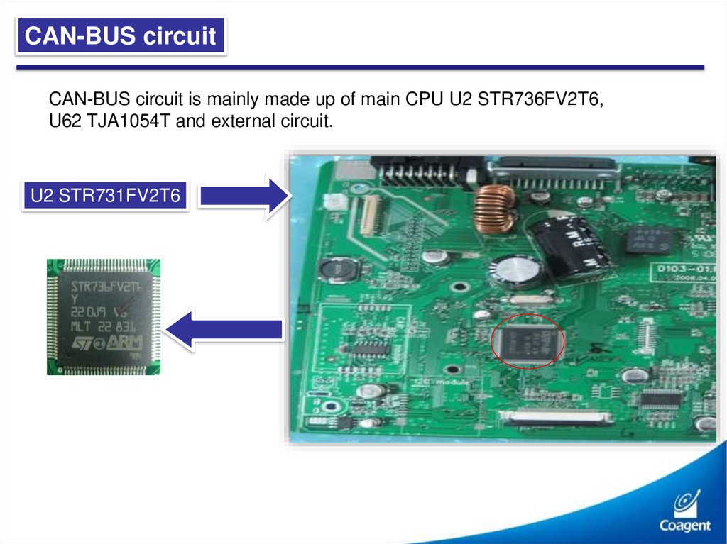
CAN-BUS circuitCAN-BUS circuit is mainly made up of main CPU U2 STR736FV2T6,
U62 TJA1054T and external circuit.
U2 STR731FV2T6
71.
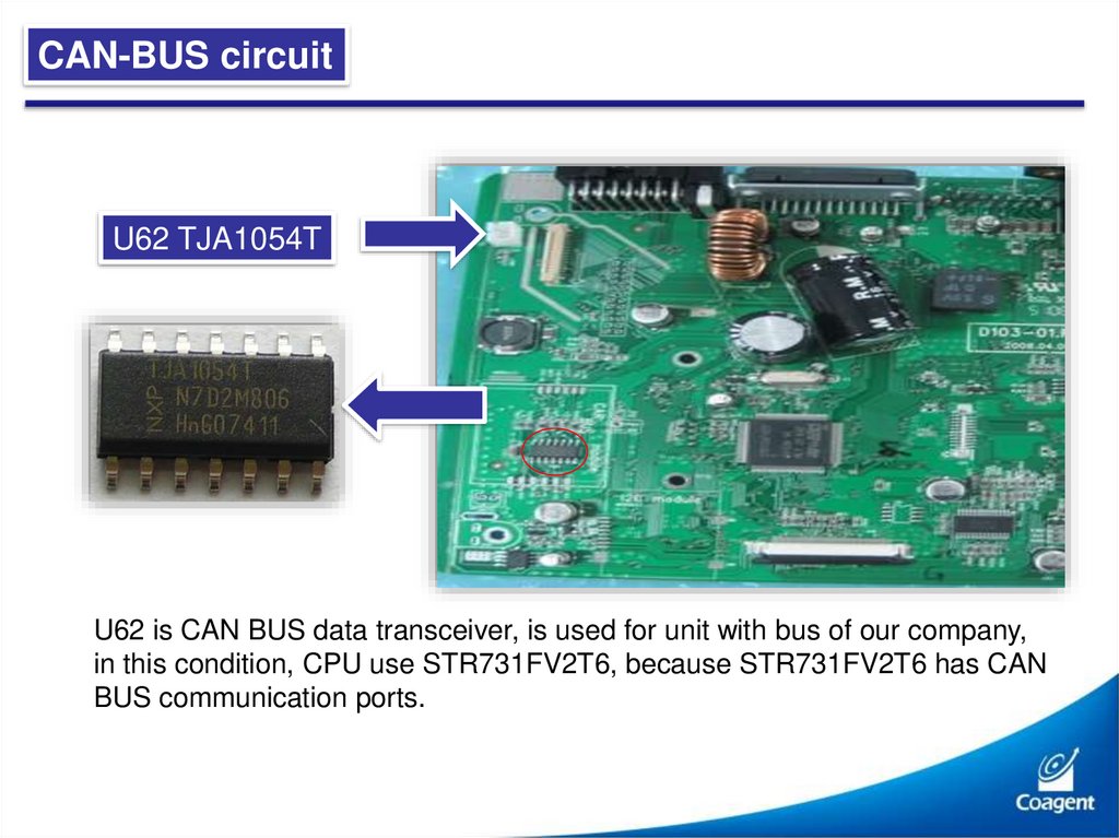
CAN-BUS circuitU62 TJA1054T
U62 is CAN BUS data transceiver, is used for unit with bus of our company,
in this condition, CPU use STR731FV2T6, because STR731FV2T6 has CAN
BUS communication ports.
72.
CAN-BUS circuitCAN-BUS circuit is mainly controlled by CPU. When detecting receive
signal, it can automatically change to receive disposing state, at this
time, U2 26th transmit bus data to U62 3rd,when detecting transmit
signal, it can automatically change to transmit disposing state, at this
time, U62 2nd transmit data to CPU 27th port, therefore, finish
communication process, U62 4th,5th,6th connect to U2 97th,98th,99th
port, finish functions like data input, output clock, 10th is power supply
port, the voltage is 5V.
1-CAN-BUS
73.
ContentsMain PCB picture
CPU controlling circuit instruction
Radio circuit instruction
Video disposing circuit instruction
Button and touch screen disposing circuit instruction
Audio disposing circuit instruction
TV circuit instruction
DVD decoding circuit instruction
CAN-BUS circuit instruction
Steering wheel learning circuit instruction
GPS circuit instruction
Virtual 6 disc circuit instruction
74.
Steering wheel learning circuitSteering wheel learning circuit is mainly made up of steering wheel
test board, connect to our unit by interface and communicate with
CPU, thus finish steering wheel learning function.
First connect steering wheel to unit, each button has each voltage in
test board, each button store different voltage, press “Setup->CONTROL
ADJUST->STEERING ADJUST”, enter to steering wheel learning interface, at this time, press “test” button, the unit start to enter to steering
wheel module test, according to unit hint, press button on steering wheel,
according to unit hint, choose function on the screen, then according
to hint, press button on steering wheel, finish learning function, and this
button stands for this function, identify by corresponding voltage,
according to this method, until all functions finish learning, after finishing
earning, you can operate functions with steering wheel.
Steering wheel learning function is mainly detecting different voltage
and storing it by CPU, thus, realize the aim to steering wheel learning
functions.
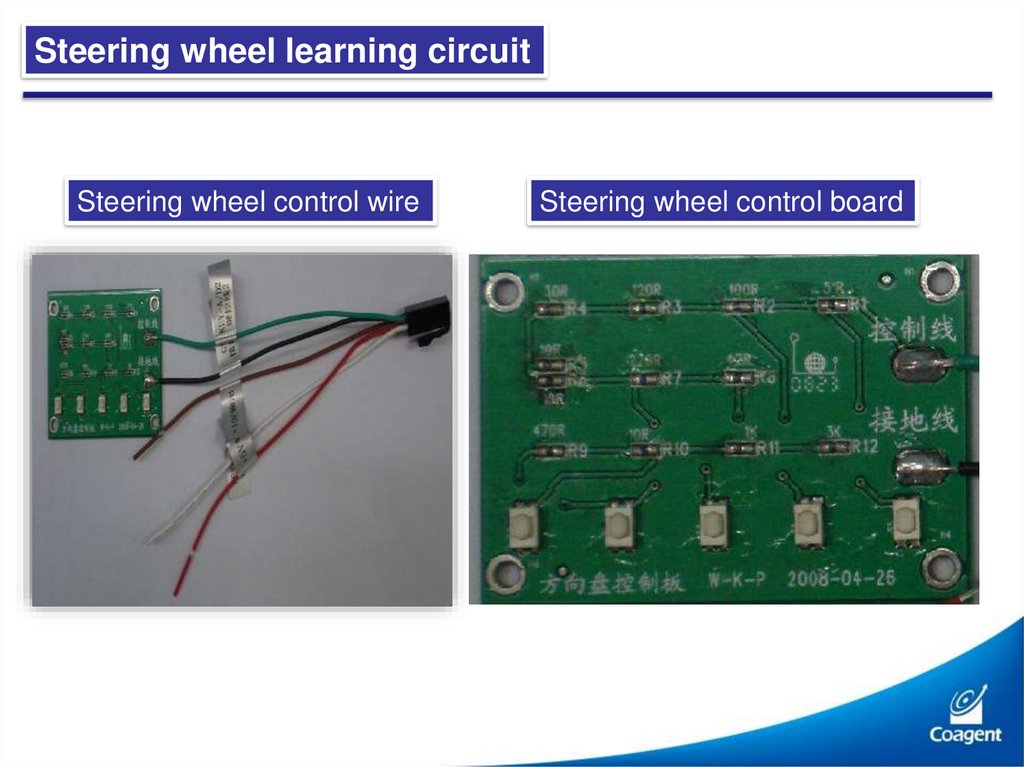
75.
Steering wheel learning circuitSteering wheel control wire
Steering wheel control board
76.
ContentsMain PCB picture
CPU controlling circuit instruction
Radio circuit instruction
Video disposing circuit instruction
Button and touch screen disposing circuit instruction
Audio disposing circuit instruction
TV circuit instruction
DVD decoding circuit instruction
CAN-BUS circuit instruction
Steering wheel learning circuit instruction
GPS circuit instruction
Virtual 6 disc circuit instruction
77.
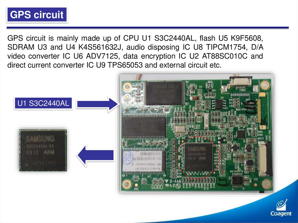
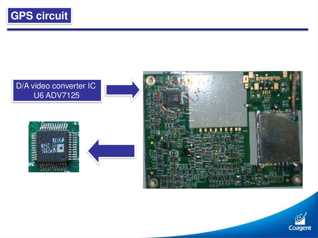
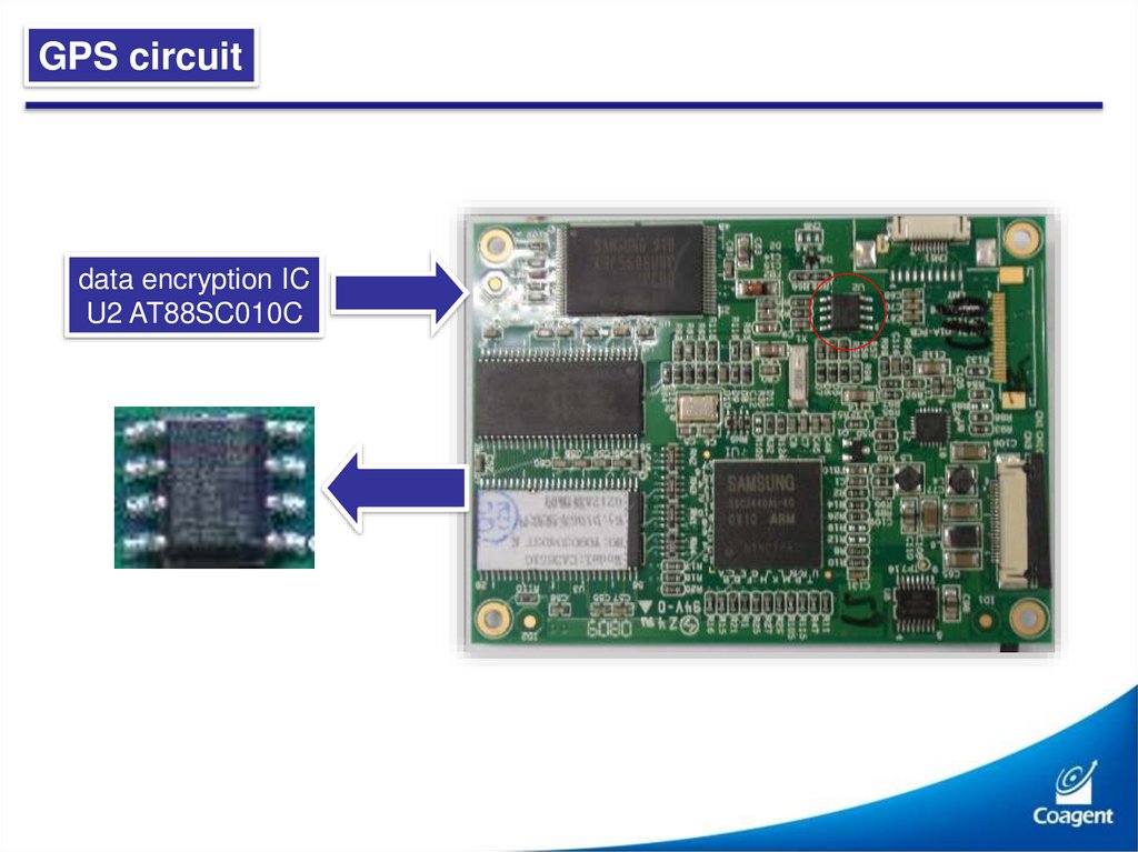
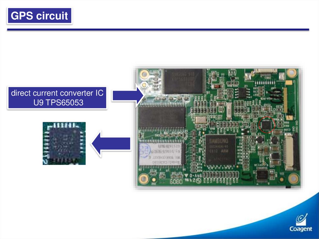
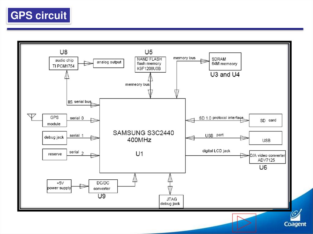
GPS circuitGPS circuit is mainly made up of CPU U1 S3C2440AL, flash U5 K9F5608,
SDRAM U3 and U4 K4S561632J, audio disposing IC U8 TIPCM1754, D/A
video converter IC U6 ADV7125, data encryption IC U2 AT88SC010C and
direct current converter IC U9 TPS65053 and external circuit etc.
U1 S3C2440AL
78.
GPS circuitflash U5 K9F5608
79.
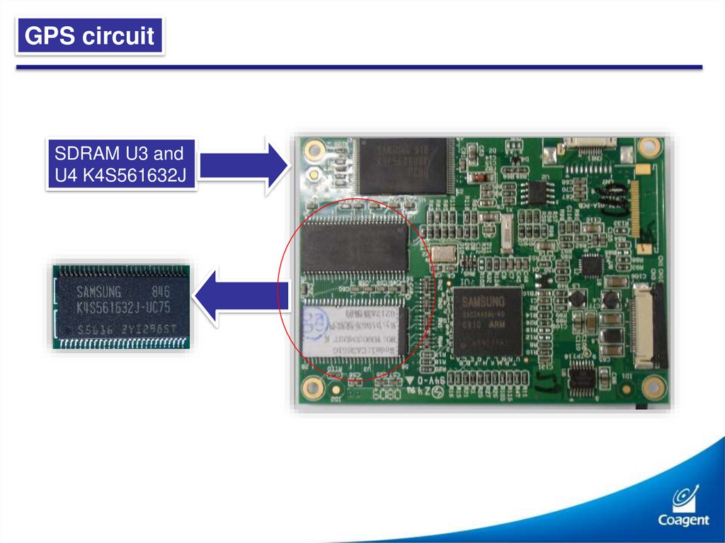
GPS circuitSDRAM U3 and
U4 K4S561632J
80.
GPS circuitaudio disposing IC
U8 TIPCM1754
81.
GPS circuitD/A video converter IC
U6 ADV7125
82.
GPS circuitdata encryption IC
U2 AT88SC010C
83.
GPS circuitdirect current converter IC
U9 TPS65053
84.
GPS circuitU1 S3C2440AL is main CPU, is mainly used for the whole circuit control and
data communication.
U5 K9F5608 is 8M flash memory, is used for storing data guiding software of
running navigation system and operation system software.
U3 and U4 K4S561632J is SDRAM flash memory, when run system, is used for
storing the buffer data that CPU pick-up from FLASH, each memory capacity
is 16M.
U8 TIPCM1754 is audio disposing chip, it communicates to CPU by serial bus,
after U8 disposing, audio signal output analog sound signal of Left/Right channel.
U6 ADV7125 is D/A (Digital/Analog) video converter IC, this chip is a A/D
converter, CPU input video signal output RGB tricolor video signal by U6
disposing and converting.
85.
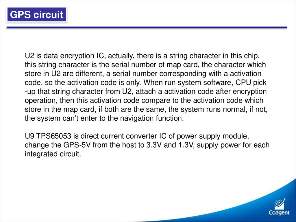
GPS circuitU2 is data encryption IC, actually, there is a string character in this chip,
this string character is the serial number of map card, the character which
store in U2 are different, a serial number corresponding with a activation
code, so the activation code is only. When run system software, CPU pick
-up that string character from U2, attach a activation code after encryption
operation, then this activation code compare to the activation code which
store in the map card, if both are the same, the system runs normal, if not,
the system can’t enter to the navigation function.
U9 TPS65053 is direct current converter IC of power supply module,
change the GPS-5V from the host to 3.3V and 1.3V, supply power for each
integrated circuit.
86.
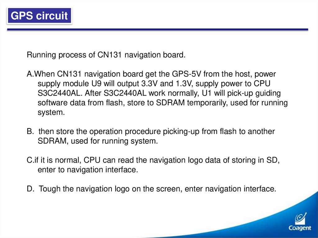
GPS circuitRunning process of CN131 navigation board.
A.When CN131 navigation board get the GPS-5V from the host, power
supply module U9 will output 3.3V and 1.3V, supply power to CPU
S3C2440AL. After S3C2440AL work normally, U1 will pick-up guiding
software data from flash, store to SDRAM temporarily, used for running
system.
B. then store the operation procedure picking-up from flash to another
SDRAM, used for running system.
C.if it is normal, CPU can read the navigation logo data of storing in SD,
enter to navigation interface.
D. Tough the navigation logo on the screen, enter navigation interface.
87.
GPS circuit88.
ContentsMain PCB picture
CPU controlling circuit instruction
Radio circuit instruction
Video disposing circuit instruction
Button and touch screen disposing circuit instruction
Audio disposing circuit instruction
TV circuit instruction
DVD decoding circuit instruction
CAN-BUS circuit instruction
Steering wheel learning circuit instruction
GPS circuit instruction
Virtual 6 disc circuit instruction
89.
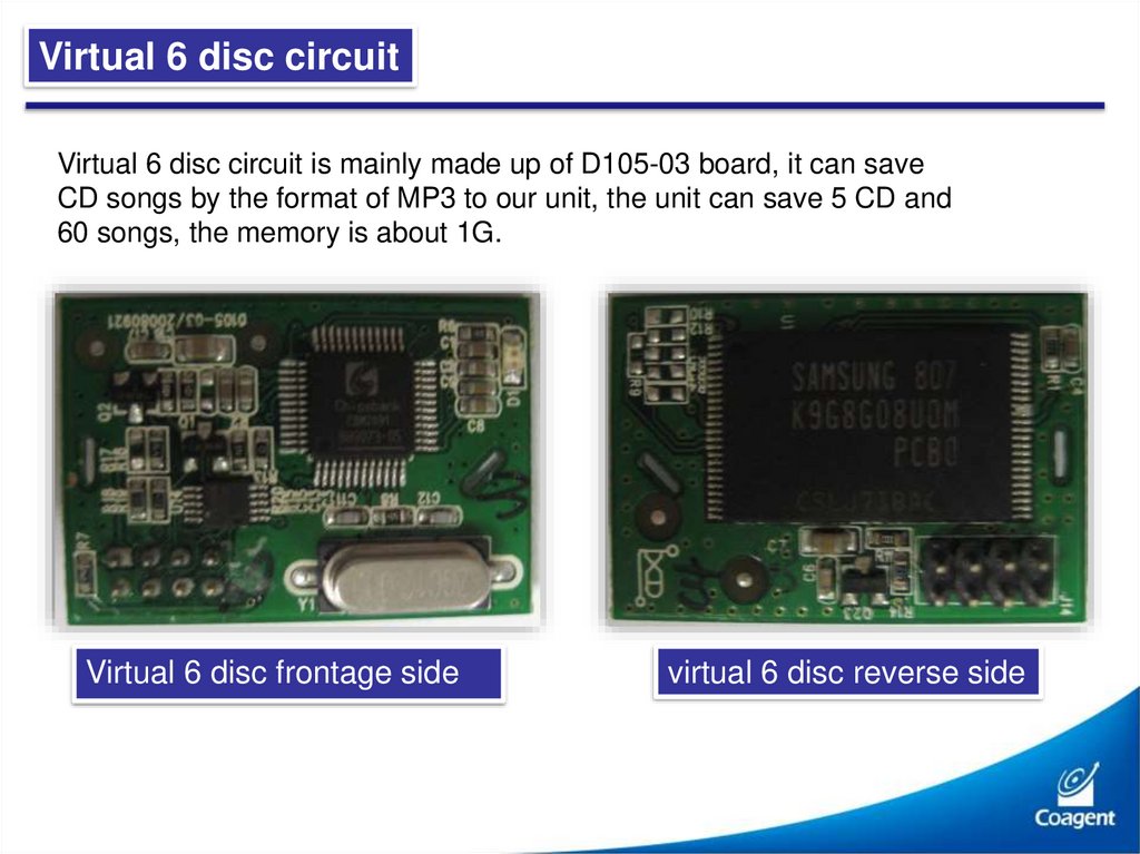
Virtual 6 disc circuitVirtual 6 disc circuit is mainly made up of D105-03 board, it can save
CD songs by the format of MP3 to our unit, the unit can save 5 CD and
60 songs, the memory is about 1G.
Virtual 6 disc frontage side
virtual 6 disc reverse side
90.
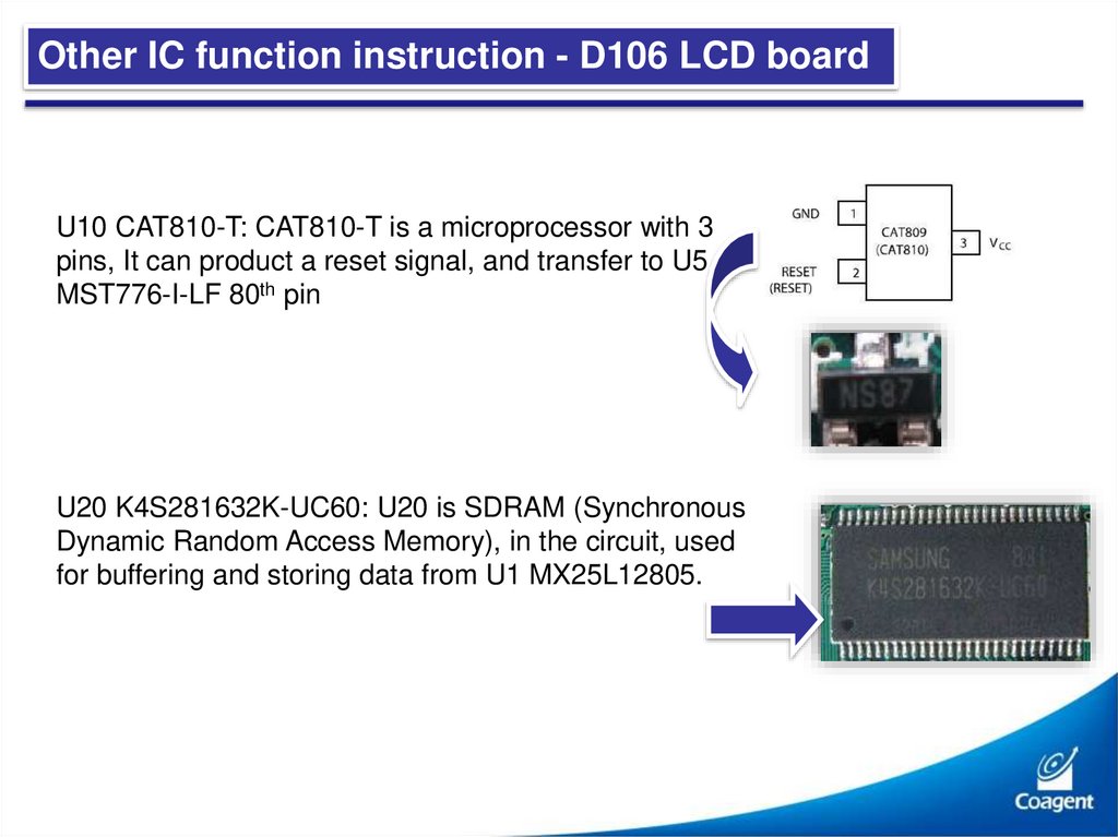
Other IC function instruction - D106 LCD boardU10 CAT810-T: CAT810-T is a microprocessor with 3
pins, It can product a reset signal, and transfer to U5
MST776-I-LF 80th pin
U20 K4S281632K-UC60: U20 is SDRAM (Synchronous
Dynamic Random Access Memory), in the circuit, used
for buffering and storing data from U1 MX25L12805.
91.
Other IC function instruction - D106 LCD boardU6 MP1540: U6 MP1540 and external elements are
made up of a DC-DC rising-voltage circuit, providing
VGH, VGL driving voltage for LCD working.
U2, U3, U4 AO3401: AO3401 is a kind of P channel
enhanced field effect transistor, in the circuit, the
function is electronic switch as voltage control element.
D3, D6, D17 BAV99: Bidirectional high-speed diode,
as high-speed switch, its exchanging time needs
only several ns
92.
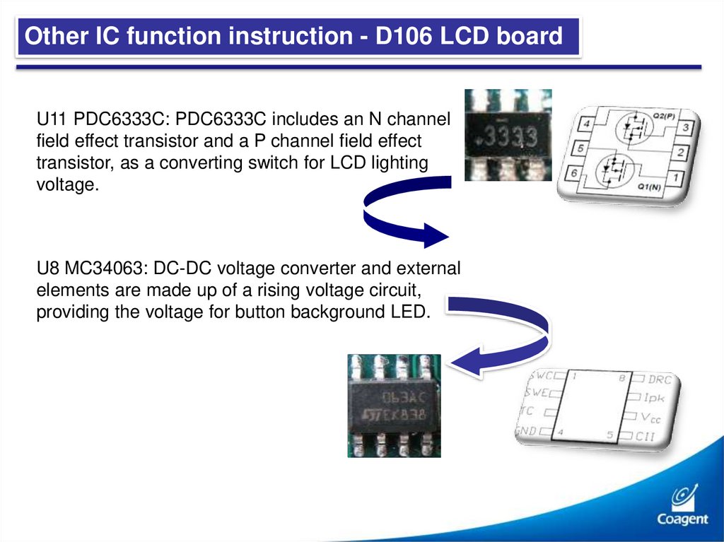
Other IC function instruction - D106 LCD boardU11 PDC6333C: PDC6333C includes an N channel
field effect transistor and a P channel field effect
transistor, as a converting switch for LCD lighting
voltage.
U8 MC34063: DC-DC voltage converter and external
elements are made up of a rising voltage circuit,
providing the voltage for button background LED.
93.
Other IC function instruction - D106 LCD boardU13 FPF2125: FPF2125 is a kind of
advantage load integrated circuit, which
has 1.8V~5.5V input voltage range,
0.15~1.5A adjustable limiting current, when
outputting current is higher than maximum
current limiting value or lower than
minimum current limited, it can output
constant current, make sure that has the
normal voltage to output in the voltage
output range.
94.
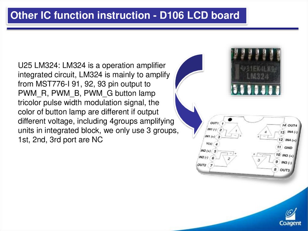
Other IC function instruction - D106 LCD boardU25 LM324: LM324 is a operation amplifier
integrated circuit, LM324 is mainly to amplify
from MST776-I 91, 92, 93 pin output to
PWM_R, PWM_B, PWM_G button lamp
tricolor pulse width modulation signal, the
color of button lamp are different if output
different voltage, including 4groups amplifying
units in integrated block, we only use 3 groups,
1st, 2nd, 3rd port are NC
95.
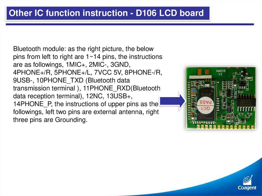
Other IC function instruction - D106 LCD boardBluetooth module: as the right picture, the below
pins from left to right are 1~14 pins, the instructions
are as followings, 1MIC+, 2MIC-, 3GND,
4PHONE+/R, 5PHONE+/L, 7VCC 5V, 8PHONE-/R,
9USB-, 10PHONE_TXD (Bluetooth data
transmission terminal ), 11PHONE_RXD(Bluetooth
data reception terminal), 12NC, 13USB+,
14PHONE_P, the instructions of upper pins as the
followings, left two pins are external antenna, right
three pins are Grounding.
96.
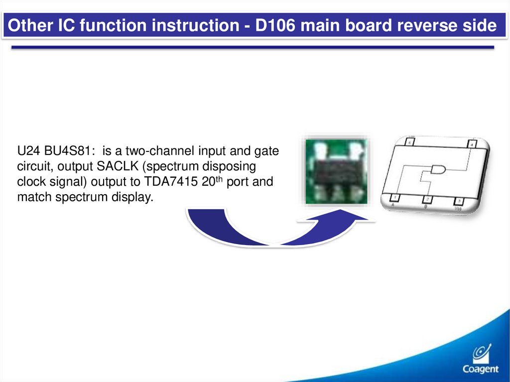
Other IC function instruction - D106 main board reverse sideU24 BU4S81: is a two-channel input and gate
circuit, output SACLK (spectrum disposing
clock signal) output to TDA7415 20th port and
match spectrum display.
97.
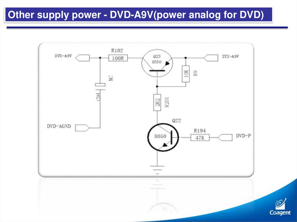
Other supply power - DVD-A9V(power analog for DVD)98.
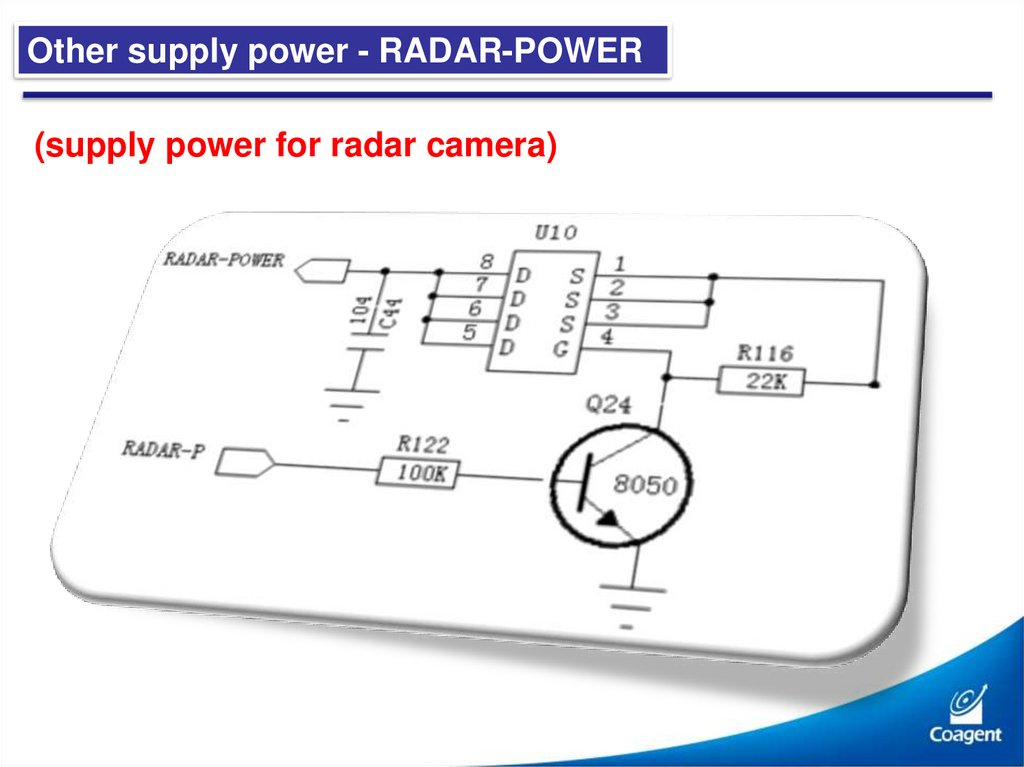
Other supply power - RADAR-POWER(supply power for radar camera)
99.
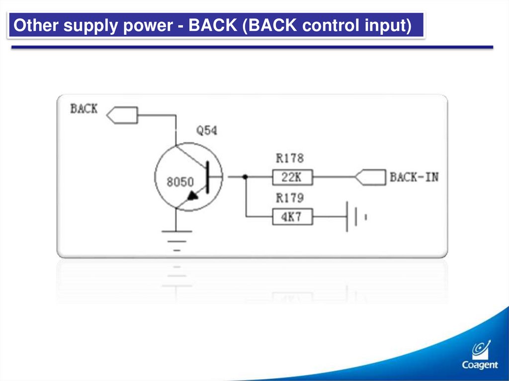
Other supply power - BACK (BACK control input)100.
Other supply power - BRAKE (BRAKE control input)101.
Other supply power - ILL (Lamp control input)102.
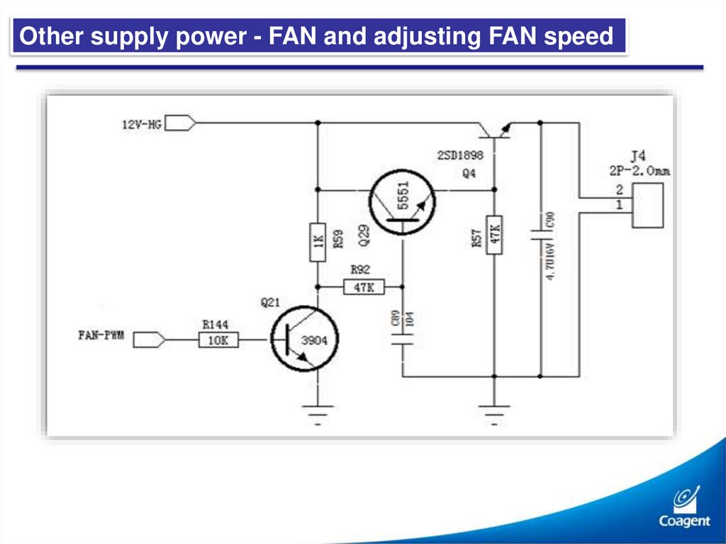
Other supply power - FAN and adjusting FAN speed103.
Other supply power - CDC-ACC (supply power for CDC)104.
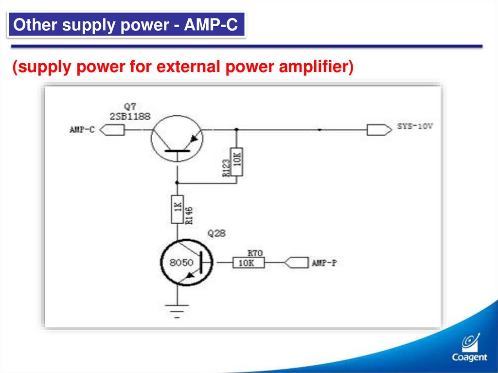
Other supply power - AMP-C(supply power for external power amplifier)
105.
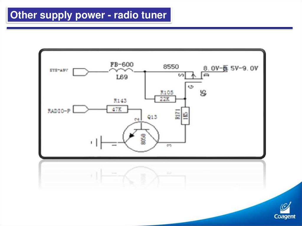
Other supply power - radio tuner106.
Other supply power - radio antenna feedback power107.
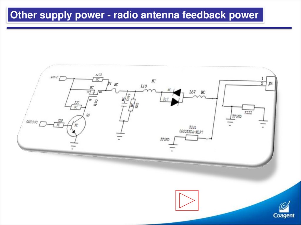
The most professional special car multimedia system supplier in the world!THANK YOU!