
")
 electronics
Similar presentations:


Resistor, inductor and capacitor in AC circuit (R-L-C reactance), Impedance (Z) and resonance
1.
Resistor, inductor andcapacitor in AC circuit
(R-L-C reactance),
Impedance (Z) and
resonance
1
2.
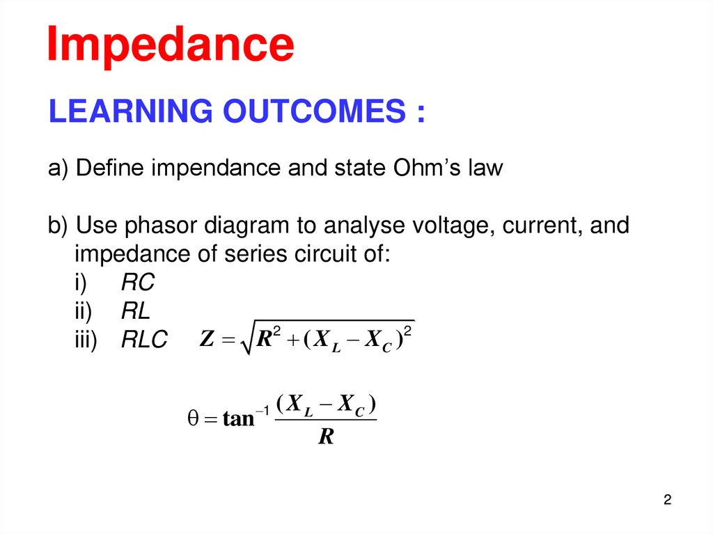
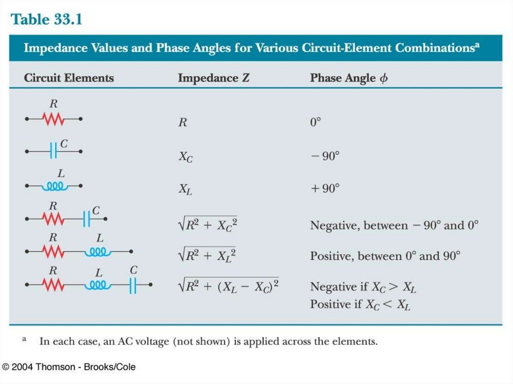
ImpedanceLEARNING OUTCOMES :
a) Define impendance and state Ohm’s law
b) Use phasor diagram to analyse voltage, current, and
impedance of series circuit of:
i) RC
ii) RL
2
2
iii) RLC Z R ( X L X C )
( X L XC )
tan
R
1
2
3. Terms used.
• Capacitive reactance• Inductor
• Inductive reactance
• Resistor
• Impedance
4.
Resistance, reactance and impedanceKey Term/Ω
Meaning
Resistance, Opposition to current flow in purely
resistive circuit.
R
Reactance,
X
Opposition to current flow resulting from
inductance or capacitance in ac
circuit.
Capacitive
reactance,Xc
Inductive
reactance,XL
Impedance,
Z
Opposition
the opposition
of a capacitor
of capacitance
to ac. to
alternating current
an opposition
the changeto
of ac.
current
Opposition
of antoinductor
through an element
Total opposition to ac.
(Resistance and reactance combine
4
to form impedance)
5.
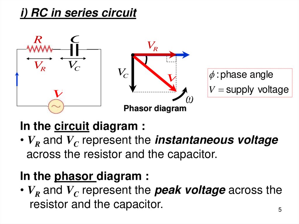
i) RC in series circuitR
C
VR
VC
V
VR
VC
: phase angle
V
ω
V supply voltage
Phasor diagram
In the circuit diagram :
• VR and VC represent the instantaneous voltage
across the resistor and the capacitor.
In the phasor diagram :
• VR and VC represent the peak voltage across the
resistor and the capacitor.
5
6. Impedance (Z)
• Impedance is the total effective resistance toan AC circuit ( Z= resistance +reactance)
• Units ohms (Ω)
• Ohms law, Vrms = IrmsZ
6
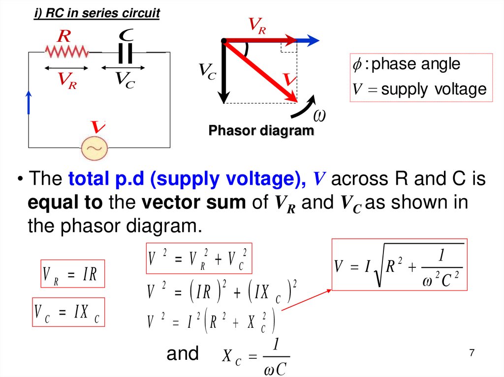
7.
i) RC in series circuitVR
C
R
VC
VC
VR
: phase angle
V
V supply voltage
ω
V
Phasor diagram
• The total p.d (supply voltage), V across R and C is
equal to the vector sum of VR and VC as shown in
the phasor diagram.
V R IR
V C IX C
V 2 V R2 V C2
V
2
IR IX C
2
V 2 I 2 R 2 X C2
and
1
V I R 2 2
ω C
2
2
1
XC
ωC
7
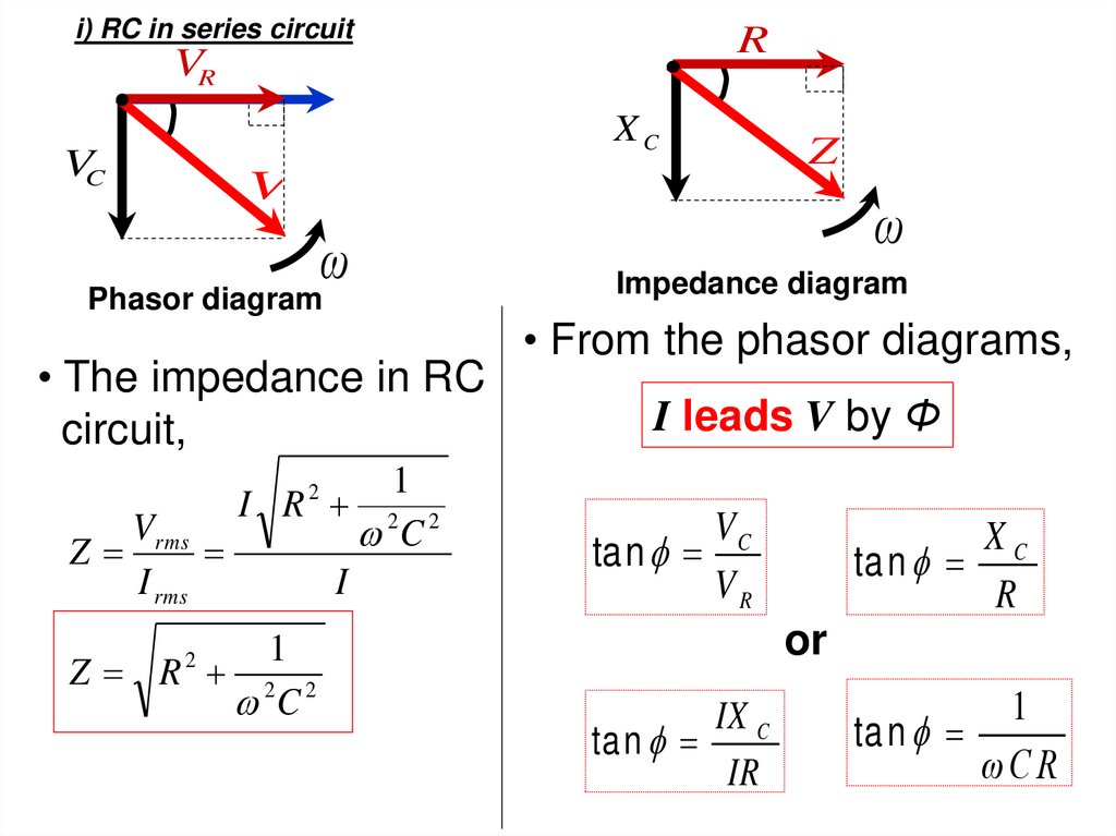
8.
i) RC in series circuitR
VR
XC
VC
V
ω
Phasor diagram
• The impedance in RC
circuit,
1
I R 2 2
V
C
Z rms
I rms
I
Z
ω
Impedance diagram
• From the phasor diagrams,
I leads V by Φ
2
1
Z R 2 2
C
VC
tan
VR
XC
ta n
R
or
2
IX C
ta n
IR
1
ta n
ωCR
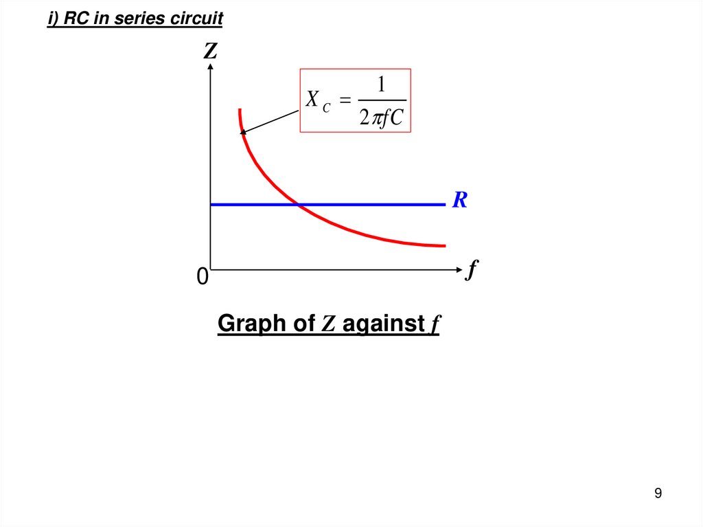
9.
i) RC in series circuitZ
1
XC
2 fC
R
f
0
Graph of Z against f
9
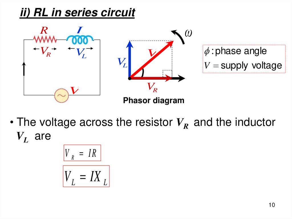
10.
ii) RL in series circuitR
L
VR
VL
V
ω
VL
V
: phase angle
V supply voltage
VR
Phasor diagram
• The voltage across the resistor VR and the inductor
VL are
V R IR
V L IX L
10
11.
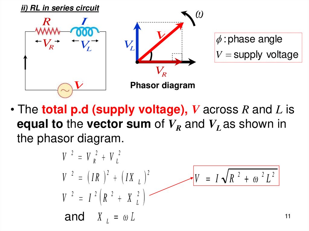
ωii) RL in series circuit
L
R
VR
V
VL
VL
: phase angle
V supply voltage
VR
V
Phasor diagram
• The total p.d (supply voltage), V across R and L is
equal to the vector sum of VR and VL as shown in
the phasor diagram.
V 2 V R2 V L2
V
2
IR IX L
2
V 2 I 2 R 2 X L2
and
X L ωL
2
V I R 2 ω 2 L2
11
12.
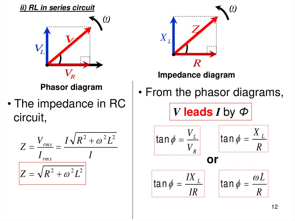
ii) RL in series circuitVL
ω
ω
XL
V
Z
R
VR
Impedance diagram
Phasor diagram
• The impedance in RC
circuit,
V rms I R L
Z
I rms
I
2
Z R 2 2 L2
2
2
• From the phasor diagrams,
V leads I by Φ
XL
ta n
R
VL
tan
VR
or
IX L
ta n
IR
ωL
ta n
R
12
13.
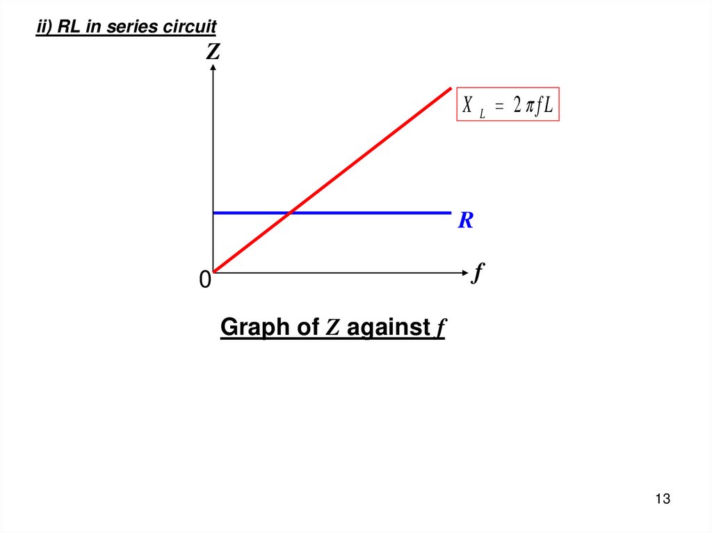
ii) RL in series circuitZ
X L 2 fL
R
f
0
Graph of Z against f
13
14.
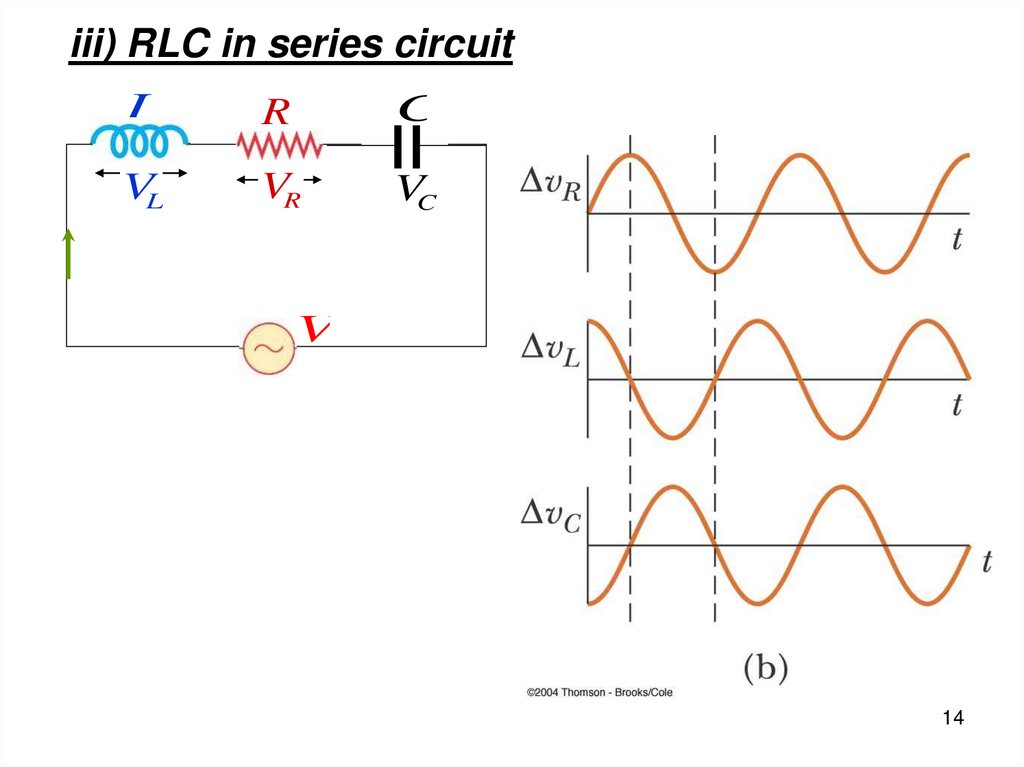
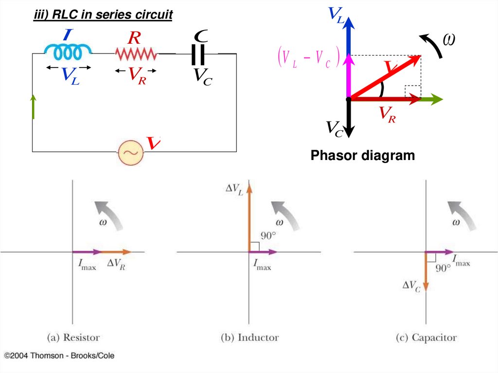
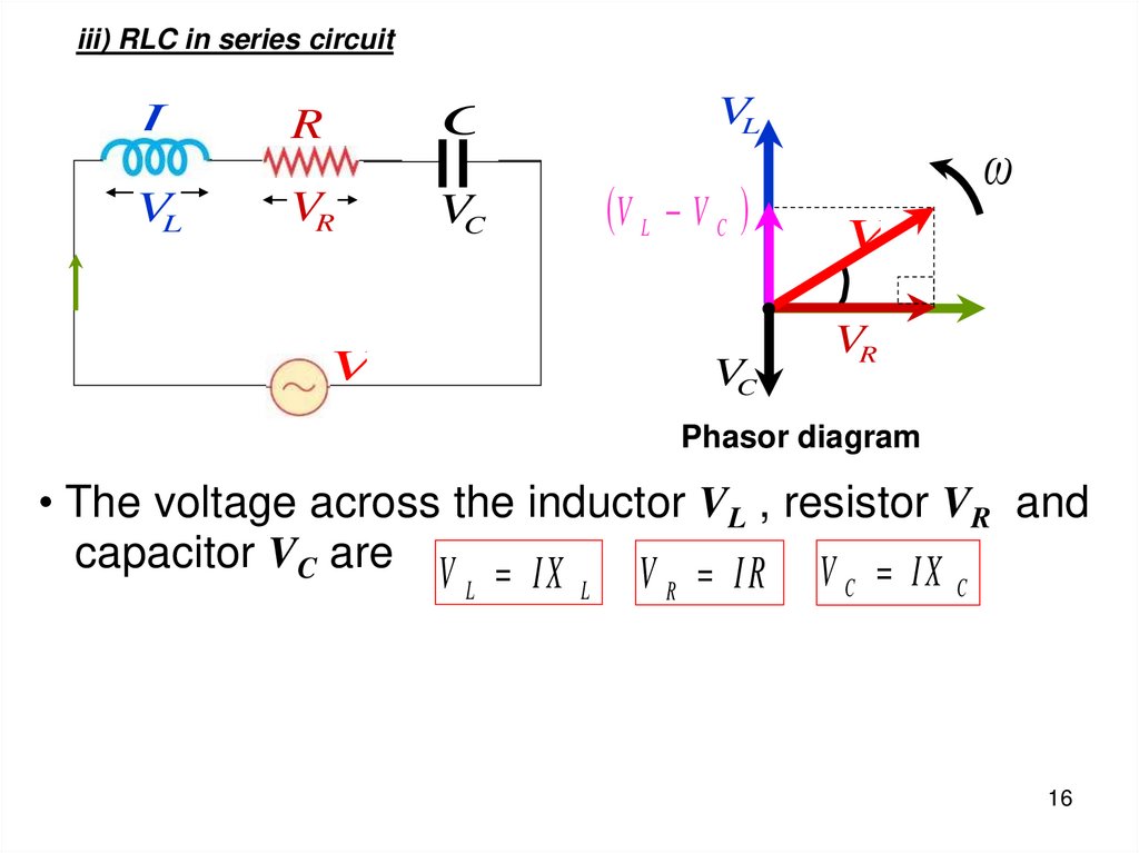
iii) RLC in series circuitL
R
C
VL
VR
VC
V
14
15.
VLiii) RLC in series circuit
L
R
C
VL
VR
VC
V
V L V C
VC
ω
V
VR
Phasor diagram
15
16.
iii) RLC in series circuitL
R
C
VL
VL
VR
VC
V L V C
V
VC
ω
V
VR
Phasor diagram
• The voltage across the inductor VL , resistor VR and
capacitor VC are V I X
V IR V IX
L
L
R
C
C
16
17.
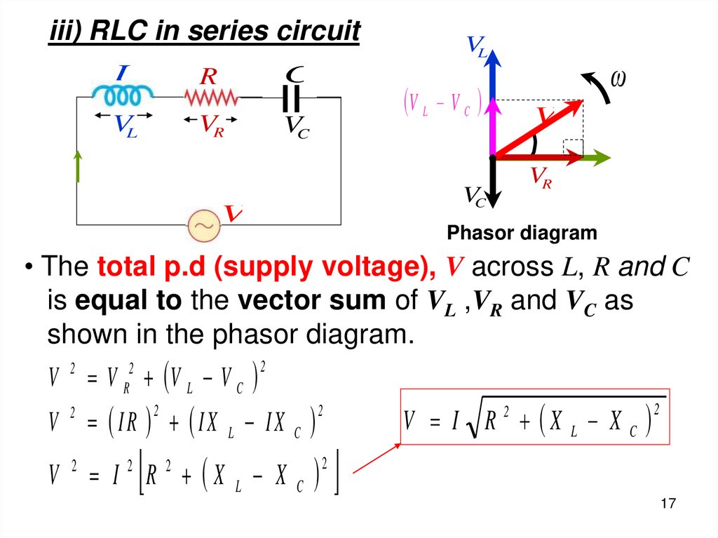
iii) RLC in series circuitL
R
C
VL
VR
VC
VL
ω
V L V C
V
VR
VC
V
Phasor diagram
• The total p.d (supply voltage), V across L, R and C
is equal to the vector sum of VL ,VR and VC as
shown in the phasor diagram.
V 2 V R2 V L V C
2
V
2
IR IX L IX C
V
2
I R X L X C
2
2
2
2
2
V I R X L X C
2
2
17
18.
XLiii) RLC in series circuit
VL
ω
V L V C
Z
V
XC
VR
VC
R
Impedance diagram
Phasor diagram
• The impedance in RLC
circuit,
V rms I R X L X C
Z
I rms
I
2
Z R X L X C
2
X L X C
ω
2
2
• From the phasor diagrams,
V leads I by Φ
V L VC
ta n
VR
I X L X C
ta n
IR
XL XC
ta n
R
1
ωL
ωC
tan
R
19.
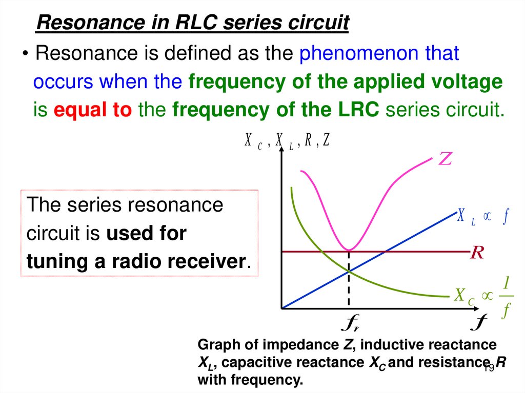
Resonance in RLC series circuit• Resonance is defined as the phenomenon that
occurs when the frequency of the applied voltage
is equal to the frequency of the LRC series circuit.
X C,X L,R,Z
Z
The series resonance
circuit is used for
tuning a radio receiver.
XL f
R
fr
1
XC
f
f
Graph of impedance Z, inductive reactance
XL, capacitive reactance XC and resistance
19R
with frequency.
20.
Resonance in RLC circuitThe graph shows that :
X C,X L,R,Z
• at low frequency, impedance Z
is large because 1/ωC is large.
• at high frequency, impedance Z
is high because ωL is large.
Z
XL f
R
fr
1
XC
f
f
• at resonance, impedance Z is minimum (Z=R)
which is
2
2
XL XC
1
2 f r L
2 f r C
resonant
frequency
fr
1
2 LC
and I is maximum
Z
R X L X C
Z min
R2 0
Z min R
V rm s V rm s
I rm s
Z
R
20
21.
2122.
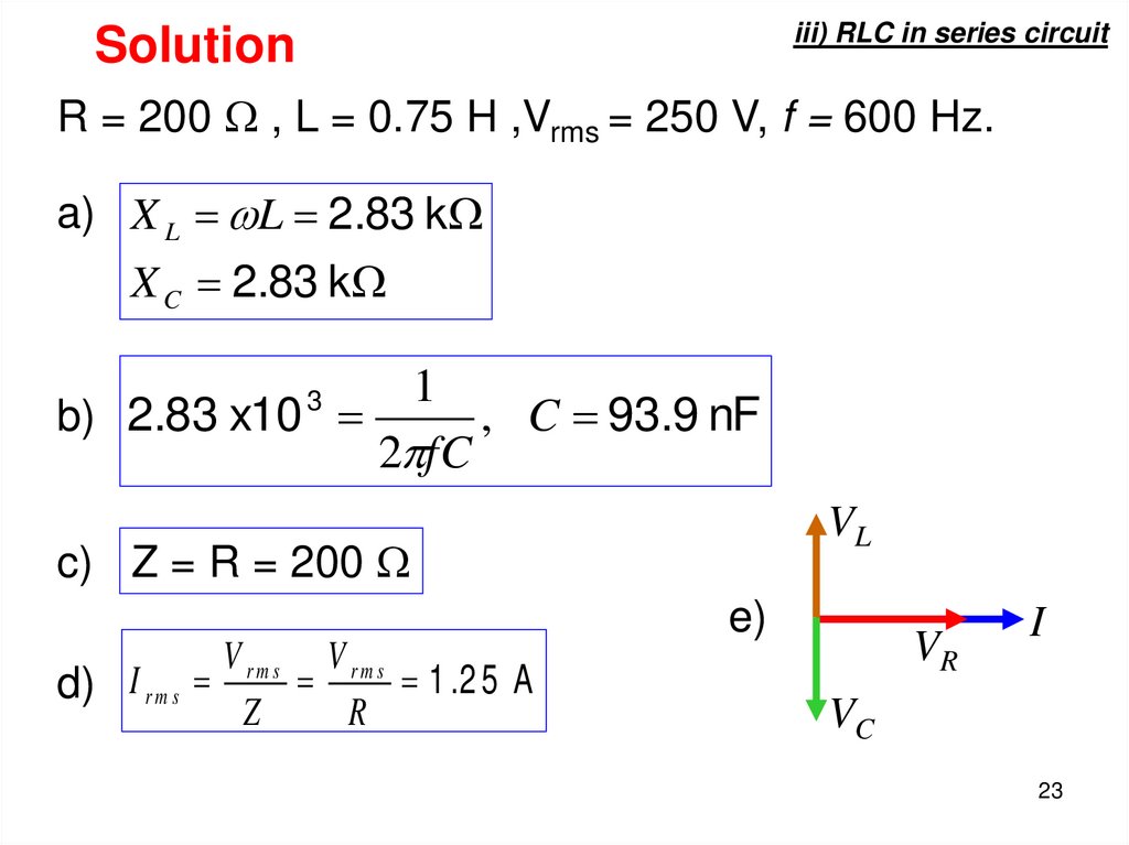
Exampleiii) RLC in series circuit
A 200 resistor, a 0.75 H inductor and a capacitor
of capacitance C are connected in series to an
alternating source 250 V, fr = 600 Hz.
Calculate
a. the inductive reactance and capacitive
reactance when resonance is occurred.
b. the capacitance C.
c. the impedance of the circuit at resonance.
d. the current flows through the circuit at
resonance.
e. Sketch the phasor diagram.
22
23.
iii) RLC in series circuitSolution
R = 200 , L = 0.75 H ,Vrms = 250 V, f = 600 Hz.
a) X L L 2.83 k
X C 2.83 k
1
b) 2.83 x10
, C 93.9 nF
2 fC
3
VL
c) Z = R = 200
e)
V rm s V rm s
1 .2 5 A
d) I r m s
Z
R
VR
I
VC
23