 electronics
Similar presentations:


Challenges and Solutions of SiC MOSFET
1.
Challenges and Solutions of SiC MOSFETMing-Jinn Tsai, 2024.4.10
2.
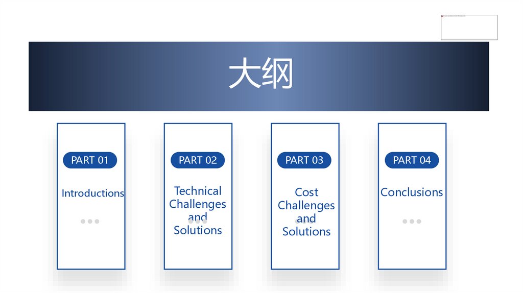
大纲PART 01
PART 02
PART 03
PART 04
Introductions
Technical
Challenges
and
Solutions
Cost
Challenges
and
Solutions
Conclusions
3.
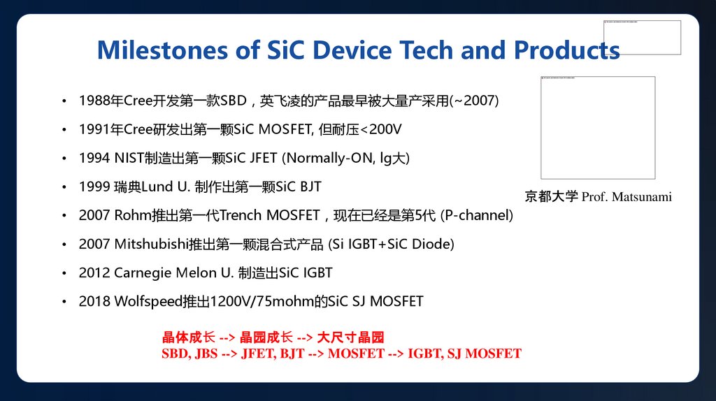
Milestones of SiC Device Tech and Products• 1988年Cree开发第一款SBD 英飞凌的产品最早被大量产采用(~2007)
• 1991年Cree研发出第一颗SiC MOSFET, 但耐压<200V
• 1994 NIST制造出第一颗SiC JFET (Normally-ON, lg大)
• 1999 瑞典Lund U. 制作出第一颗SiC BJT
• 2007 Rohm推出第一代Trench MOSFET 现在已经是第5代 (P-channel)
• 2007 Mitshubishi推出第一颗混合式产品 (Si IGBT+SiC Diode)
• 2012 Carnegie Melon U. 制造出SiC IGBT
• 2018 Wolfspeed推出1200V/75mohm的SiC SJ MOSFET
晶体成长 --> 晶园成长 --> 大尺寸晶园
SBD, JBS --> JFET, BJT --> MOSFET --> IGBT, SJ MOSFET
京都大学 Prof. Matsunami
4.
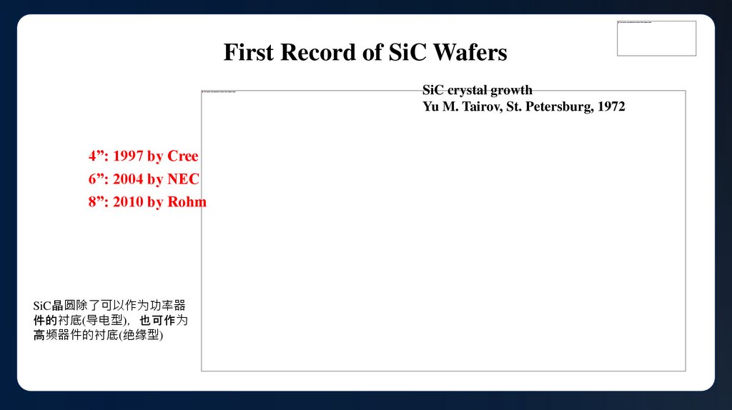
First Record of SiC WafersSiC crystal growth
Yu M. Tairov, St. Petersburg, 1972
4”: 1997 by Cree
6”: 2004 by NEC
8”: 2010 by Rohm
SiC晶圆除了可以作为功率器
件的衬底(导电型) 也可作为
高频器件的衬底(绝缘型)
5.
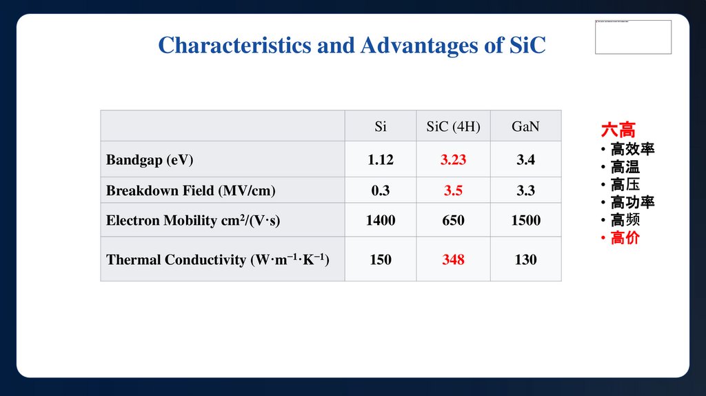
Characteristics and Advantages of SiCSi
SiC (4H)
GaN
Bandgap (eV)
1.12
3.23
3.4
Breakdown Field (MV/cm)
0.3
3.5
3.3
Electron Mobility cm2/(V·s)
1400
650
1500
Thermal Conductivity (W·m−1·K−1)
150
348
130
六高
• 高效率
• 高温
• 高压
• 高功率
• 高频
• 高价
6.
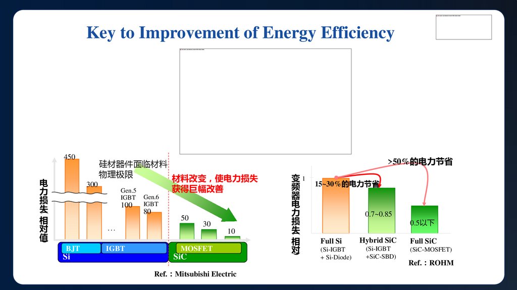
Key to Improvement of Energy Efficiency450
300
Gen.5
IGBT
100
(
…
获得巨幅改善
Gen.6
IGBT
80
50
30
10
)
Si
IGBT
MOSFET
SiC
Ref. Mitsubishi Electric
变1
频
器
电
力
损
失
相
对
)
BJT
>50%的电力节省
15~30%的电力节省
0.7~0.85
0.5以下
(
电
力
损
失
相
对
值
硅材器件面临材料
物理极限
材料改变 使电力损失
Full Si
(Si-IGBT
+ Si-Diode)
Hybrid SiC
(Si-IGBT
+SiC-SBD)
Full SiC
(SiC-MOSFET)
Ref. ROHM
7.
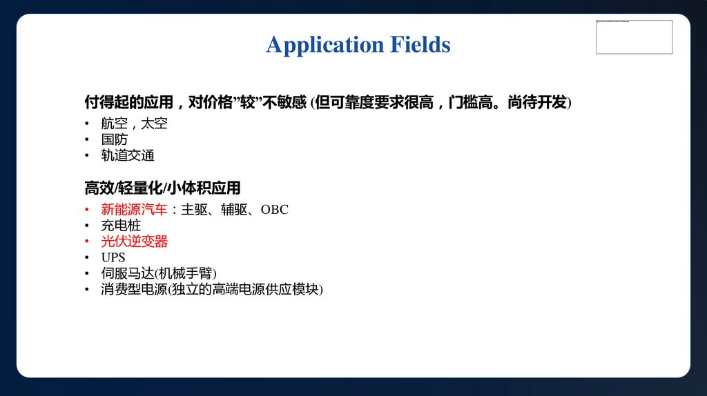
Application Fields付得起的应用 对价格”较”不敏感 (但可靠度要求很高 门槛高。尚待开发)
• 航空 太空
• 国防
• 轨道交通
高效/轻量化/小体积应用
新能源汽车 主驱、辅驱、OBC
充电桩
光伏逆变器
UPS
伺服马达(机械手臂)
消费型电源(独立的高端电源供应模块)
8.
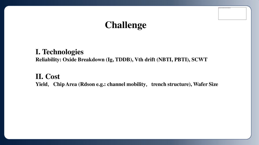
ChallengeI. Technologies
Reliability: Oxide Breakdown (Ig, TDDB), Vth drift (NBTI, PBTI), SCWT
II. Cost
Yield Chip Area (Rdson e.g.: channel mobility trench structure), Wafer Size
9.
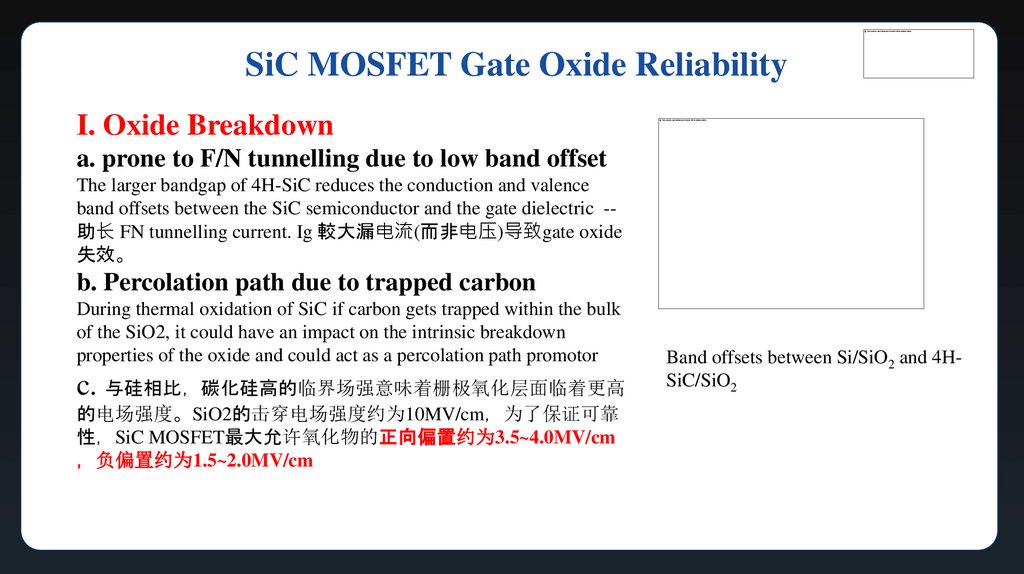
SiC MOSFET Gate Oxide ReliabilityI. Oxide Breakdown
a. prone to F/N tunnelling due to low band offset
The larger bandgap of 4H-SiC reduces the conduction and valence
band offsets between the SiC semiconductor and the gate dielectric -助长 FN tunnelling current. Ig 較大漏电流(而非电压)导致gate oxide
失效。
b. Percolation path due to trapped carbon
During thermal oxidation of SiC if carbon gets trapped within the bulk
of the SiO2, it could have an impact on the intrinsic breakdown
properties of the oxide and could act as a percolation path promotor
c. 与硅相比 碳化硅高的临界场强意味着栅极氧化层面临着更高
的电场强度。SiO2的击穿电场强度约为10MV/cm 为了保证可靠
性 SiC MOSFET最大允许氧化物的正向偏置约为3.5~4.0MV/cm
负偏置约为1.5~2.0MV/cm
Band offsets between Si/SiO2 and 4HSiC/SiO2
10.
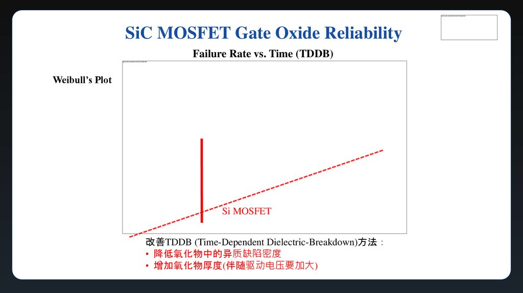
SiC MOSFET Gate Oxide ReliabilityFailure Rate vs. Time (TDDB)
Weibull’s Plot
Si MOSFET
改善TDDB (Time-Dependent Dielectric-Breakdown)方法
• 降低氧化物中的异质缺陷密度
• 增加氧化物厚度(伴随驱动电压要加大)
11.
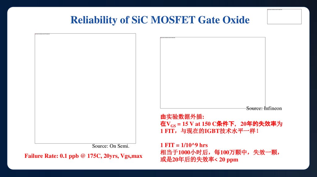
Reliability of SiC MOSFET Gate OxideSource: Infineon
由实验数据外插:
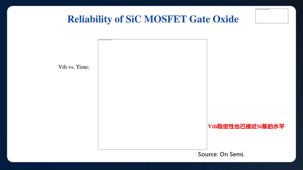
在VGS = 15 V at 150 C条件下 20年的失效率为
1 FIT 与现在的IGBT技术水平一样
Source: On Semi.
Failure Rate: 0.1 ppb @ 175C, 20yrs, Vgs,max
1 FIT = 1/10^9 hrs
相当于1000小时后 每100万颗中 失效一颗
或是20年后的失效率< 20 ppm
12.
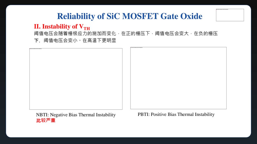
Reliability of SiC MOSFET Gate OxideII. Instability of VTH
阈值电压会随着栅极应力的施加而变化 在正的栅压下 阈值电压会变大 在负的栅压
下 阈值电压会变小。在高温下更明显
NBTI: Negative Bias Thermal Instability
比较严重
PBTI: Positive Bias Thermal Instability
13.
Reliability of SiC MOSFET Gate OxideVth vs. Time:
Vth稳定性也已接近Si基的水平
Source: On Semi.
14.
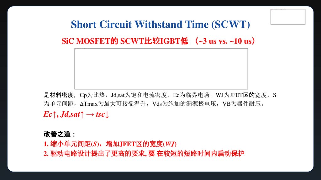
Short Circuit Withstand Time (SCWT)SiC MOSFET的 SCWT比较IGBT低 ~3 us vs. ~10 us
是材料密度 Cp为比热 Jd,sat为饱和电流密度 Ec为临界电场 WJ为JFET区的宽度 S
为单元间距 ΔTmax为最大可接受温升 Vds为施加的漏源极电压 VB为器件耐压。
Ec↑, Jd,sat↑ → tsc↓
改善之道
1. 缩小单元间距(S) 增加JFET区的宽度(WJ)
2. 驱动电路设计提出了更高的要求, 要 在较短的短路时间内启动保护
15.
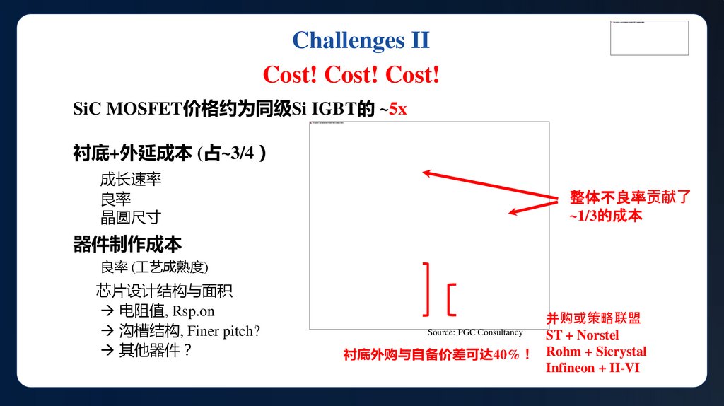
Challenges IICost! Cost! Cost!
SiC MOSFET价格约为同级Si IGBT的 ~5x
衬底+外延成本 (占~3/4
成长速率
良率
晶圆尺寸
整体不良率贡献了
~1/3的成本
器件制作成本
良率 (工艺成熟度)
芯片设计结构与面积
电阻值, Rsp.on
沟槽结构, Finer pitch?
其他器件
并购或策略联盟
Source: PGC Consultancy
ST + Norstel
衬底外购与自备价差可达40% Rohm + Sicrystal
Infineon + II-VI
16.
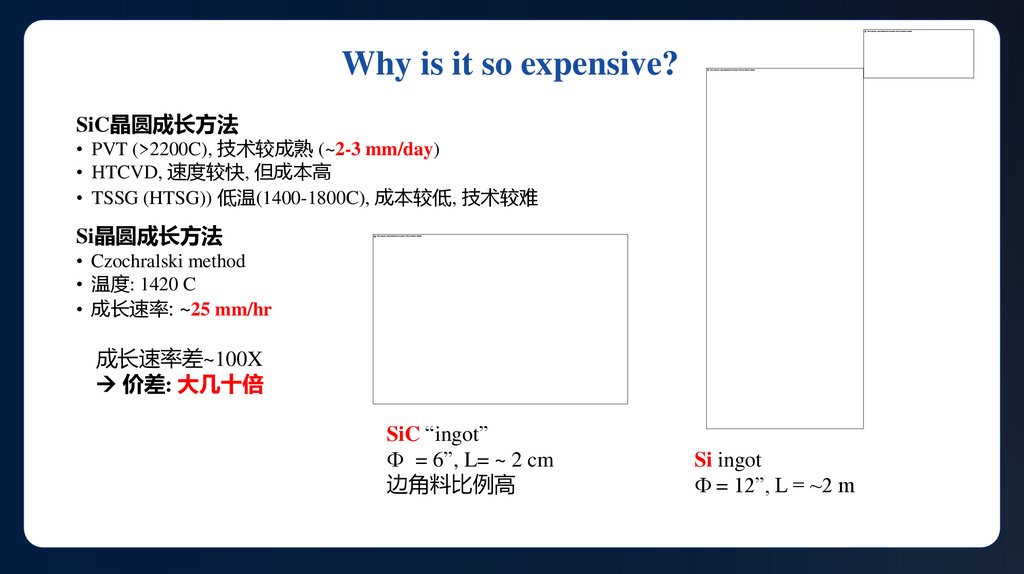
Why is it so expensive?SiC晶圆成长方法
• PVT (>2200C), 技术较成熟 (~2-3 mm/day)
• HTCVD, 速度较快, 但成本高
• TSSG (HTSG)) 低温(1400-1800C), 成本较低, 技术较难
Si晶圆成长方法
• Czochralski method
• 温度: 1420 C
• 成长速率: ~25 mm/hr
成长速率差~100X
价差: 大几十倍
SiC “ingot”
= 6”, L= ~ 2 cm
边角料比例高
Si ingot
= 12”, L = ~2 m
17.
RDS(ON) is not what’s expectedRDS(ON)*A ~ 3 - 5 mΩxmm2 (@VG=15-18V)
Rch 大于理想值 因为低的Channel Mobility
bulk mobility: ~ 400 cm²/Vs
channel mobility: 5 – 70 cm²/Vs
1. Dit of SiC/SiO2: ~1011-12 cm-2V-1
Dit of Si/SiO2: ~1010 cm-2V-1
2. 界面粗糙度: 因为EPI成长的需要晶圆方向与晶格面有4°斜角
改善方案
1. ”适当的栅氧成长与退火” 可以
a. 降低 Dit
b. 增加channel mobility.
c. 同时改善NBTI与PBTI
2. Adopting trench structure
3. Wafer thinning to reduce Rdrift
18.
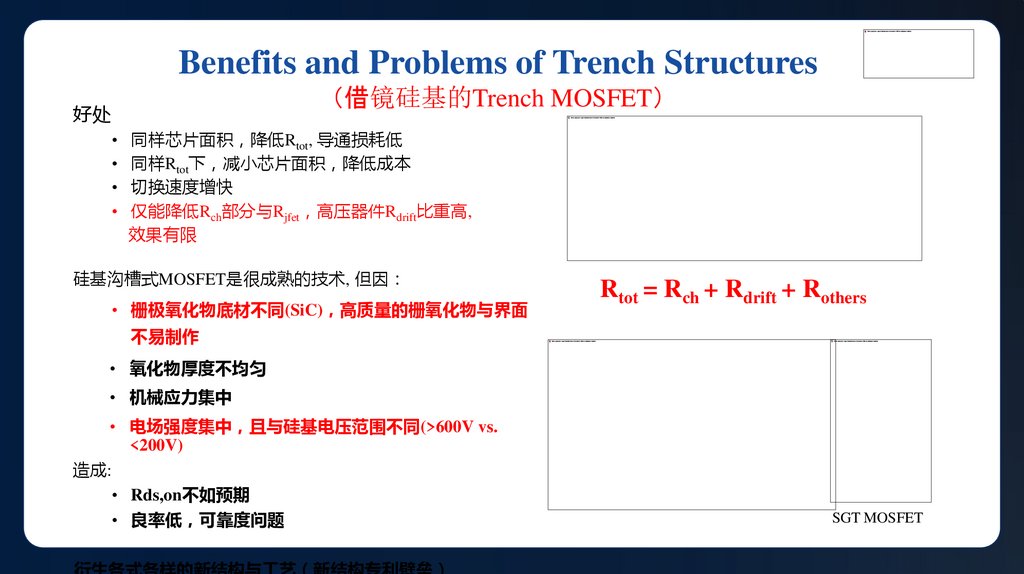
Benefits and Problems of Trench Structures借镜硅基的Trench MOSFET
好处
同样芯片面积 降低Rtot, 导通损耗低
同样Rtot下 减小芯片面积 降低成本
切换速度增快
仅能降低Rch部分与Rjfet 高压器件Rdrift比重高,
效果有限
硅基沟槽式MOSFET是很成熟的技术, 但因
• 栅极氧化物底材不同(SiC) 高质量的栅氧化物与界面
Rtot = Rch + Rdrift + Rothers
不易制作
• 氧化物厚度不均匀
• 机械应力集中
• 电场强度集中 且与硅基电压范围不同(>600V vs.
<200V)
造成:
• Rds,on不如预期
• 良率低 可靠度问题
衍生各式各样的新结构与工艺 新结构专利壁垒
SGT MOSFET
19.
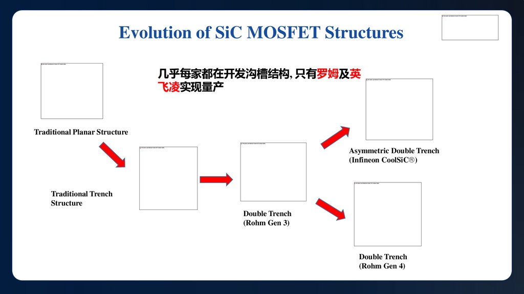
Evolution of SiC MOSFET Structures几乎每家都在开发沟槽结构, 只有罗姆及英
飞凌实现量产
Traditional Planar Structure
Asymmetric Double Trench
(Infineon CoolSiC )
Traditional Trench
Structure
Double Trench
(Rohm Gen 3)
Double Trench
(Rohm Gen 4)
20.
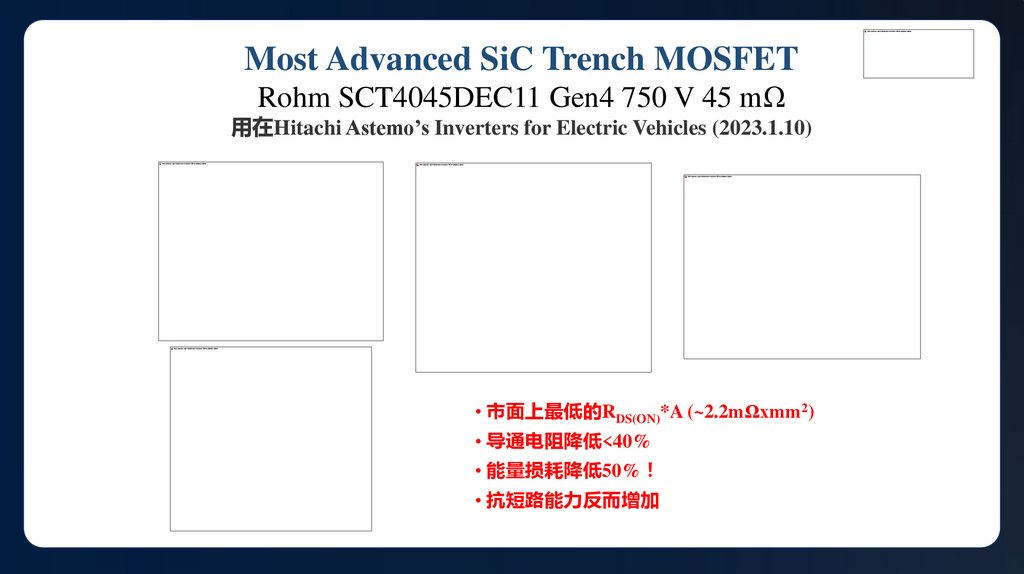
Most Advanced SiC Trench MOSFETRohm SCT4045DEC11 Gen4 750 V 45 mΩ
用在Hitachi Astemo’s Inverters for Electric Vehicles (2023.1.10)
• 市面上最低的RDS(ON)*A (~2.2mΩxmm2)
• 导通电阻降低<40%
• 能量损耗降低50%
• 抗短路能力反而增加
21.
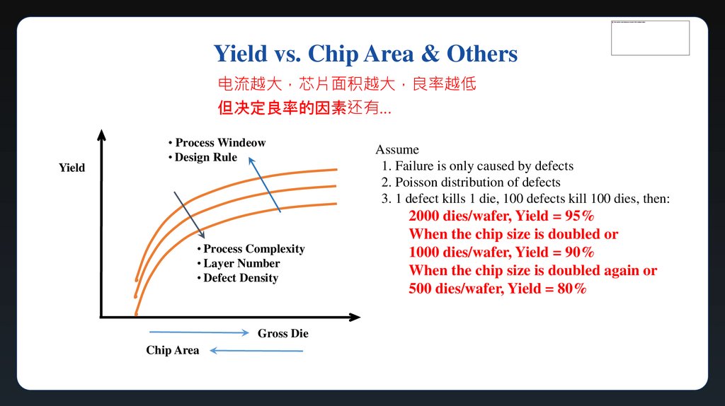
Yield vs. Chip Area & Others电流越大 芯片面积越大 良率越低
但决定良率的因素还有...
Yield
• Process Windeow
• Design Rule
• Process Complexity
• Layer Number
• Defect Density
Gross Die
Chip Area
Assume
1. Failure is only caused by defects
2. Poisson distribution of defects
3. 1 defect kills 1 die, 100 defects kill 100 dies, then:
2000 dies/wafer, Yield = 95%
When the chip size is doubled or
1000 dies/wafer, Yield = 90%
When the chip size is doubled again or
500 dies/wafer, Yield = 80%
22.
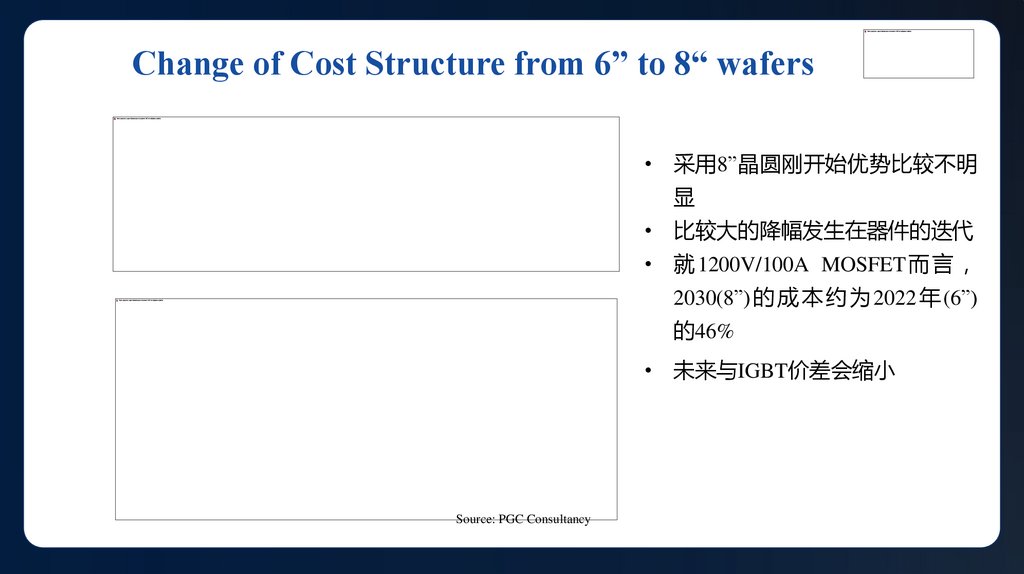
Change of Cost Structure from 6” to 8“ wafers• 采用8”晶圆刚开始优势比较不明
显
• 比较大的降幅发生在器件的迭代
• 就 1200V/100A MOSFET 而 言
2030(8”) 的 成 本 约 为 2022 年 (6”)
的46%
• 未来与IGBT价差会缩小
Source: PGC Consultancy
23.
Conclusions• Market and application fields and market of SiC MOSFET grows rapidly
• Expensive, but Yield in substrate growth and device fabrication can reduce cost
greatly (>1/3)
• Trench structure can reduce Rdson and so the chip area and cost.
• Reliability and low SCWT issues require extra protection consideration in the gate
driver and controller
• Transition from 6” to 8” wafer is a trend but it depends on the maturity of the
technologies and supply chain