 industry
Similar presentations:


")


Memristors based on heteroepitaxial SiGe structures
1.
UNN PSSN RECMemristors based on heteroepitaxial SiGe structures
Dmitrii Filatov, Мaria Shenina, Ivan Antonov, Valentina Kotomina, Dmitrii Antonov, Alexander Kruglov, Dmitrii Pavlov,
Vladislav Vorontsov, Vladimir Shengurov, Sergei Denisov, Margarita Ryabova, Oleg Gorshkov
WELCOME TO NANOWORLD
dmitry_filatov@inbox.ru
Lobachevskii University of Nizhnii Novgorod, Nizhnii Novgorod, Russia
The work is devoted to investigation of the resistive switching (RS) in the novel type memristors – so-called Epitaxial Resistive Random Access Memory
(EpiRRAM) devices based on the Me/Si-Ge/Si(001) stacks (Me = Ag, Ru) with relaxed Si and Ge epitaxial layers (ELs). In such devices, the conductive filaments
(CFs) are the chains of the Me atoms filling the cores of threading dislocations growing though Si and Ge ELs. The prototype memristors based on the p-Ge/n+Si(001), low-doped p-Si/p-Ge/n+-Si(001), and p-Ge/p-Si(001)/n+-Si(001) heterostructures were studied.
Materials and methods
Introduction. Memristors are the elements of a new generation of nonvolatile computer memory [1] and neuromorphic computing systems [2].
Recently, a new type of memristors based on epitaxial Si0.9Ge0.1/Si(001)
heterostructures (Epitaxial RRAM or EpiRRAM) was demonstrated [3].
We have shown that the Ag/Ge/Si(001) memristor structures exhibit
nonvolatile RS associated with the formation of conductive filaments
from Ag atoms in the threading dislocations in the Ge EL [4]. The lateral
confinement of the CFs inside the dislocation cores was expected to
improve the RS stability and endurance.
The RS of the prototype memristors
based on p-Ge/n+-Si(001), p--Si/pGe/n+-Si(001), and p-Ge/pSi(001)/n+-Si(001) heterostructures
with 60x60 μm2 mesas and the top
electrodes of Ag and Ru were studied
using Agilent B1500A semiconductor
device analyzer in the dc voltage
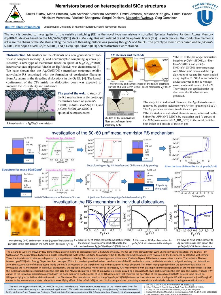
Morphology and current image of the top Ag electrode
sweep mode with a step of ~1 mV.
surface of p-Si/p-Ge/n+-Si(001) based memristor Vg=-0.1 V
The voltage was applied to the top
electrode, the Si substrate was
grounded.
The goal of the wok: to study of
the RS mechanism in the prototype
memristors based on p-Ge/n+Si(001), p--Si/p-Ge/n+-Si(001), and
p-Ge/p-Si(001)/n+-Si(001)
epitaxial heterostructures
Studies of RS in individual
filaments of memristor
stacks by AFM
RS mechanism in Ag/Ge/Si memristors
To study RS in individual filamenst, the Ag electrodes were
removed by grazing incidence (~3°) Ar+ ion sputtering (2 keV).
The Ag particles remained inside the etch pits.
The RS studies in individual filaments were performed on the
Solver Pro AFM (NT-MDT), by measuring the I-V curves of
the AFMprobe contact (HA_HR_DCP) to the metal particles
both inside and outside of the etch pits
Investigation of the 60 60 μm2 mesa memristor RS mechanism
i-Si
(40 nm)
i-Si
(40 nm)
p-Ge
(100 nm)
p-Ge
(100
nm)
n+-Si
n+-Si
Electroforming on Ag/ i-Si interface and CB filament of Ag growing
Structure for mesa 60 60μm2
RS on the base of diode-like I-V of p-n Ge/n+-Si
Ru (50 nm)
Ru (50 nm)
i-Si
(80 nm)
i-Si
(80 nm)
p-Ge
(80 nm)
p-Ge
(80 nm)
n+-Si
RS polarity
changing [5]
n+-Si
Initial CB-like amount of Ru ions in Si layer
Injection of Ru ions into p-Si/p-Ge interface during RS
4
10
3
10
2
10
1
2
It (nA)
10
9
6
3
0
-3
-6
-9
1
It (nA)
It (nA)
Investigation the RS mechanism in individual dislocations
10
4
10
3
10
2
10
1
RESET
SET
-0,05 0,00 0,05
Vg (V)
0
10
-1,0
-0,5
0,0
Vg (V)
0,5
0
10
-1,5 -1,0 -0,5 0,0 0,5 1,0 1,5
1,0
Vg (V)
.Morphology (left) and current image (right) of individual Ag I-V curves of AFM probe contact to Ag particle inside A I-V curve of AFM probe contact to
the etch pit on p-Ge/n+-Si stack (1) and to the
p-Ge/n+-Si structure outside etch pits
particles in the etch pitss on the Ag/p-Ge/n+-Si strack Vg=+4В
micron-sized mesa Ag/p--Si/p-Ge/n+-Si(001) stack (2)
I-V curve of AFM probe contact to
Ag particle inside etch pit on the
p-Ge/p-Si/n+-Si heterostructure
The Ge and Si ELs were grown by low-temperature growth methods compatible with Si CMOS technology. The Ge ELs were grown by Hot Wire Chemical Vapor deposition, the Si ones – by
Sublimation Molecular Beam Epitaxy in a single technological cycle at the substrate temperature 325 C. The threading dislocations were revealed on the EL surfaces by selective wet etching.
Then, the top Me electrodes were deposited by magnetron sputtering. The fabricated prototype memristors manifested a bipolar RS between two resistance states. Transmission Electron
Microscopy (TEM) with Energy Dispersion Spectroscope (EDS) microanalysis provided a direct confirmation of the RS mechanism based on the Me ion electromigration along the dislocations.
Also, the accumulation of the Me atoms inside the misfit dislocations at the Ge/Si interface in the course of RS was observed. This effect may potentially limit the EpiRRAM durability. To
investigate the RS mechanism in individual dislocations, we applied Conductive Atomic Force Microscopy (CAFM) combined with grazing incidence ion sputtering of the Me electrodes so that
the metal nanoparticles remained inside the etch pits. The AFM probe played a role of a movable electrode providing a contact to the Me particles inside the etch pits. The current-voltage (I-V)
curves of the individual dislocations agreed with the ones measured on the mesas of 60 by 60 mkm in size that confirms the operation of the prototype EpiRRAM devices to be based on
filling/emptying of individual dislocations with the Me atoms. The memristors based on the p-Si/p-Ge/n+-Si(001) heterostructures demonstrated the bipolar RS with asymmetric (rectifying) I-V
curves in the low-resistance state related to the rectifying effect of the p-Ge/n+-Si junction. Such a design allows combining a memristor and a diode selector in a single monolithic stack.
This work was supported by RFBR, 19-29-03026 mk., Russian Federation, "Memristor structures based on the SiGe epritaxial layers for
resistive nonvolatile memory and neuromorphic applications". The studies were carried out using the equipment of the shared research
facility of Research and Educational Center for Physics of Solid-State Nanostructures at N.I. Lobachevsky State University of Nizhny Novgorod
1 S.H. Lee, X. Zhu, W.D. Lu. Nano Research, 13, 1228 (2020).
2 J. Zhu, T. Zhang, Y. Yang, R. Huang. Appl. Phys. Rev., 7, 011312 (2020).
3 S. Choi, S.H. Tan et al.// Nature Materials, V.17, P.335-340 (2018).
4 Filatov D.O., Shenina M.E.et al. // Semiconductors. V.54. No.14. P.1833- 1835 (2020).
5 J. H. Yoon et.al. // Adv. Mater., V.2020. P.1904599 (2020).