Similar presentations:
Structural, substructural properties and chemical composition
1.
Structural, substructural properties and chemical compositionof flexible ZnO films deposited by nanoink spray printing
O. Dobrozhan, O. Diachenko, R. Pshenychnyi, D. Kurbatov, A. Opanasyuk
Department of Electronics and Computer Technology, Sumy State University
dobrozhan.a@gmail.com, opanasyuk_sumdu@ukr.net
Motivation
o Era of modern flexible microelectronic devices, particularly flexible solar cells, thermoelectric generators and
sensors;
o Functional elements based on ZnO semiconductor material due to excellent physico-chemical properties are
widely used in development of microelectronic devices;
o Nanoink spray printing approach to develop flexible ZnO films are low-cost, versatile, scalable allowing to
design functional elements with programmed fundamental properties;
o Functional and performance features (e.g. energy conversion efficiency, sensitivity, stability, reproducibility) of
flexible ZnO based microelectronic devices are strongly related to fundamental properties (crystal structure,
phase and chemical composition, substructural and optical properties).
World class flexible solar cell,
thermoelectric generator and sensor
Steps to develop flexible ZnO films
Nanocrystal synthesis
EG
ZnO NCs
Zinc acetate + EG
(0.2 M)
Spray printing
Nanoink formation
Nanocrystals
+
Organic matrix
(glycols, alcohols, binders)
=
Nanoinks
(viscosity, wettability, surface
tension)
Functional elements
Spraying parameters:
• Air conditions;
• Polyamide substrate (8 x 8 cm);
• 150 °C substrate temperature;
• 20 printing cycles (spraying - 3
s, pause - 5 s);
• Annealing at 200-400 °C for
10-60 min in Ar atm.
Polyamide
Polyester
Mo
SiO2
ZnO films onto flexible
(polyamide, polyester) and
rigid (Mo, SiO2) substrates.
Fundamental properties of flexible ZnO films
Structure and substructure
Morphology and chemical composition
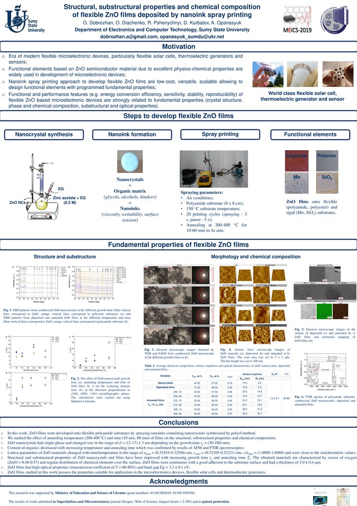
Fig. 1. XRD patterns from synthesized ZnO nanocrystals at the different growth time (blue vertical
lines correspond to ZnO; orange vertical lines correspond to polyester substrate) (a) and
XRD patterns from deposited and annealed ZnO films at the different temperature and time
(blue vertical lines correspond to ZnO; orange vertical lines correspond to polyamide substrate (b).
Fig. 5. Electron microscopic images of the
surface of deposited (a) and annealed (b, c)
ZnO films and elemental mapping of
ZnO films (d).
Fig. 4. Atomic force microscope images of
ZnO nanoink (a), deposited (b) and annealed (c-h)
ZnO films. The scan area was set to 2 x 2 μm.
The bar height was set to 200 nm.
Table 2. Average chemical composition, surface roughness and optical characteristics of ZnO nanocrystals, deposited
and annealed films.
Fig. 3. Electron microscopic images obtained by
TEM and SAED from synthesized ZnO nanocrystals
at the different growth times (a-d).
CZn, at.%
CO, at.%
Zn/O
Nanocrystals
42.50
57.50
Deposited films
31.50
200, 10
Samples
Fig. 2. The effect of ZnO nanocrystals growth
time (a), annealing temperature and time of
ZnO films (b, c) on the scattering domain
sizes (L) in the direction perpendicular to
(100), (002), (101) crystallographic planes.
The calculations were carried out using
Scherrer’s formula.
Surface roughness
Rms (nm)
Ra (nm)
0.74
10.5
8.8
68.50
0.46
12.6
9.5
32.50
67.50
0.48
20.5
14.8
200, 60
33.50
66.50
0.50
18.4
15.7
Annealed films,
275, 10
33.50
66.50
0.50
23.2
18.1
Тa, С; ta, min
275, 60
34.60
65.40
0.53
25.1
19.3
400, 10
35.60
64.40
0.55
38.2
31.2
400, 60
36.50
63.50
0.57
43.2
32.7
Eg, eV
T, %
3.3 ± 0.1
60-80
Fig. 6. FTIR spectra of polyamide substrate,
synthesized ZnO nanocrystals, deposited and
annealed films.
Conclusions
o
o
o
o
o
o
o
o
In this work, ZnO films were developed onto flexible polyamide substrates by spraying nanoinks containing nanocrystals synthesized by polyol method;
We studied the effect of annealing temperature (200-400 °C) and time (10 min, 60 min) of films on the structural, substructural properties and chemical composition;
ZnO nanocrystals had single-phase and changed size in the range of d = (12-17) ± 3 nm depending on the growth time tg = (30-180) min;
Content of organics decreased with increasing temperature and annealing time which was confirmed by results of AFM and FTIR spectroscopies;
Lattice parameters of ZnO materials changed with time/temperature in the range of aZnO = (0.32454-0.32588) nm, сZnO = (0.52105-0.52221) nm, c/aZnO = (1.6000-1.6080) and were close to the stoichiometric values;
Structural and substructural properties of ZnO nanocrystals and films have been improved with increasing growth time tg and annealing time Ta. The obtained materials are characterized by excess of oxygen
(Zn/O = 0.46-0.57) and regular distribution of chemical elements over the surface. ZnO films were continuous with a good adhesion to the substrate surface and had a thickness of 2.0 ± 0.4 μm;
ZnO films had high optical properties (transmission coefficient of T = 60-80%) and band gap Eg = 3.3 ± 0.1 eV;
ZnO films studied in this work possess the properties suitable for application in the microelectronics devices, flexible solar cells and thermoelectric generators.
Acknowledgments
This research was supported by Ministry of Education and Science of Ukraine (grant numbers: 0116U002619, 0119U100398).
The results of work submitted to Superlattices and Microstructures journal (Scopus, Web of Science, Impact factor = 2.385) and to patent protection.

 chemistry


