


 physics
Similar presentations:


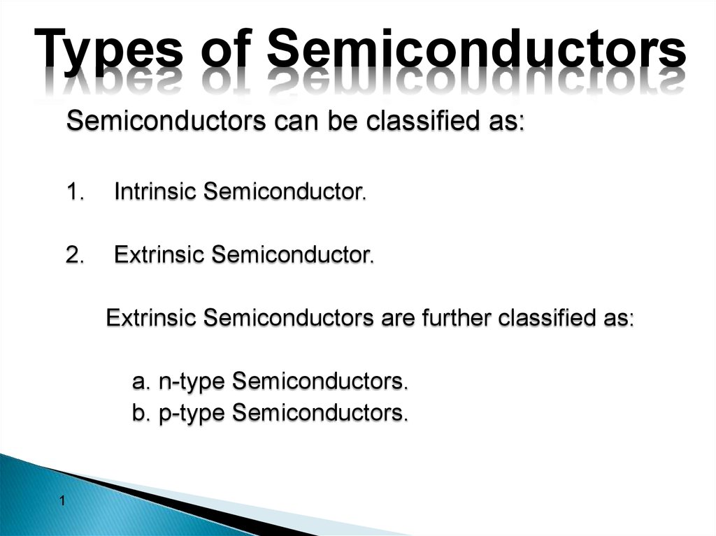
Types of Semiconductors
1.
Types of SemiconductorsSemiconductors can be classified as:
1.
Intrinsic Semiconductor.
2.
Extrinsic Semiconductor.
Extrinsic Semiconductors are further classified as:
a. n-type Semiconductors.
b. p-type Semiconductors.
1
2. Intrinsic Semiconductor
SiSi
Si
FREE ELECTRON
Si
Si
Si
HOLE
Si
Si
Semiconductor in pure
form is known as
Intrinsic Semiconductor.
Ex. Pure Germanium,
Pure Silicon.
At room temp. no of
electrons equal to no. of
holes.
Si
Fig 1.
2
3. Intrinsic semiconductor energy band diagram
Conduction BandEnergy in ev
FERMI
LEVEL
Valence Band
Fig 2.
Fermi level lies in the middle
3
4. Extrinsic Semiconductor
4When we add an impurity to pure semiconductor to
increase the charge carriers then it becomes an
Extrinsic Semiconductor.
In extrinsic semiconductor without breaking the
covalent bonds we can increase the charge carriers.
5. Comparison of semiconductors
Intrinsic Semiconductor1. It is in pure form.
2. Holes and electrons are
equal.
3. Fermi level lies in between
valence and conduction
Bands.
4. Ratio of majority and
minority carriers is unity.
Extrinsic Semiconductor
1. It is formed by adding trivalent
or pentavalent impurity to a pure
semiconductor.
2.No. of holes are more in p-type
and no. of electrons are more in ntype.
3. Fermi level lies near
valence band in p-type and
near conduction band in n-type.
4. Ratio of majority and
minority carriers are equal.
5
6. Comparison between n-type and p-type semiconductors
P-typeN-type
6
Pentavalent impurities
are added.
Majority carriers are
electrons.
Minority carriers are
holes.
Fermi level is near the
conduction band.
Trivalent impurities are
added.
Majority carriers are
holes.
Minority carriers are
electrons.
Fermi level is near the
valence band.
7. N-type Semiconductor
7When we add a pentavalent
impurity to pure semiconductor
we get n-type semiconductor.
Arsenic atom has 5 valence
electrons.
Fifth electron is superfluous,
becomes free electron and
enters into conduction band.
Therefore pentavalent impurity
donates one electron and
becomes positive donor ion.
Pentavalent impurity known as
donor.
N-type
Si
As
Fig 1.
8. P-type Semiconductor
8When we add a Trivalent impurity
to pure semiconductor we get ptype semiconductor.
Gallium atom has 3 valence
electrons.
It makes covalent bonds with
adjacent three electrons of silicon
atom.
There is a deficiency of one
covalent bond and creates a hole.
Therefore trivalent impurity
accepts one electron and becomes
negative acceptor ion. Trivalent
impurity known as acceptor.
P-type
Si
Ga
Fig 2.
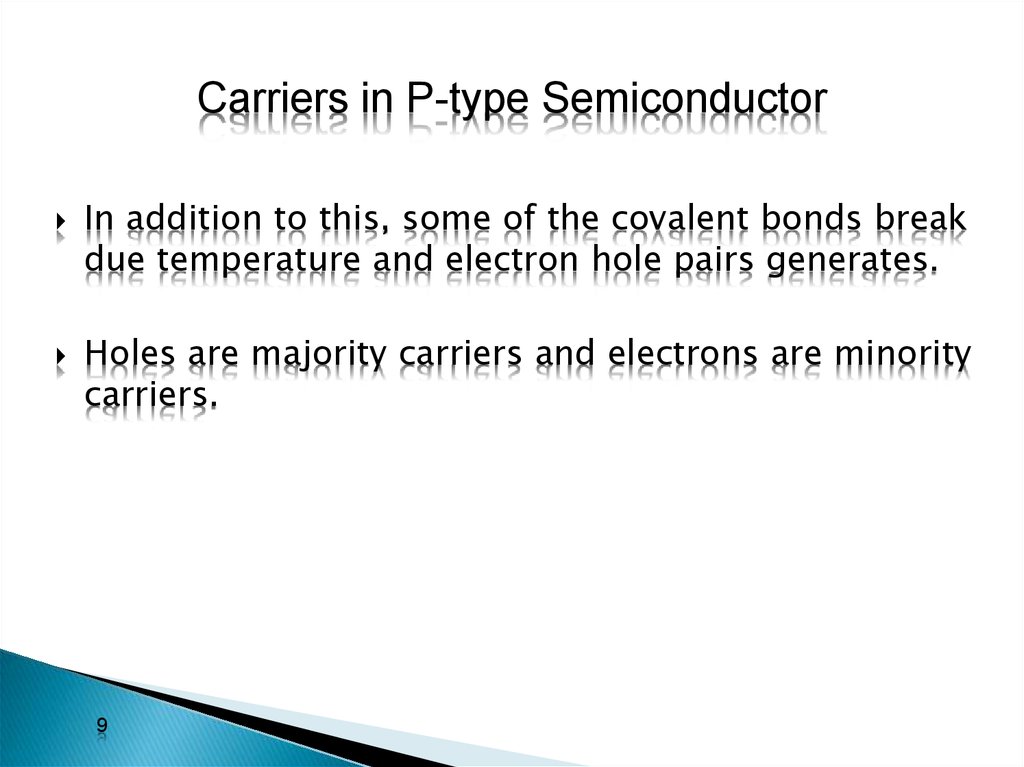
9.
Carriers in P-type SemiconductorIn addition to this, some of the covalent bonds break
due temperature and electron hole pairs generates.
Holes are majority carriers and electrons are minority
carriers.
9
10. P and N type Semiconductors
Acceptor ionP
Donor ion
-
-
-
-
+
+
+
+
-
-
-
-
+
+
+
+
-
-
+
+
Minority electron
Majority holes
Majority electrons
Fig 3.
10
N
+
Minority hole
11. Comparison of semiconductors
Intrinsic SemiconductorIt is in pure form.
1.
2.
3.
11
Extrinsic Semiconductor
1.
Holes and electrons
are equal.
2.
Fermi level lies in
between valence and
conduction Bands.
3.
It formed by adding trivalent
or pentavalent impurity to a
pure semiconductor.
No. of holes are more in ptype and no. of electrons are
more in n-type.
Fermi level lies near valence
band in p-type and near
conduction band in n-type.
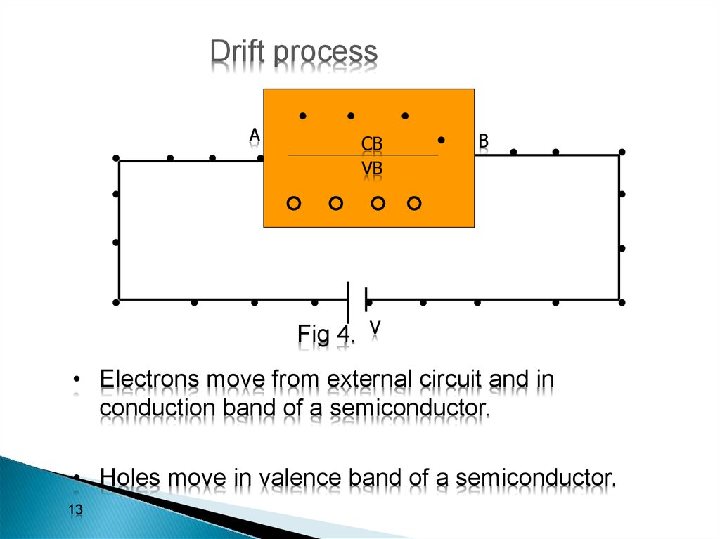
12. Conduction in Semiconductors
Conduction is carried out by means of1. Drift Process.
2. Diffusion Process.
12
13.
Drift processA
CB
VB
Fig 4.
B
V
• Electrons move from external circuit and in
conduction band of a semiconductor.
• Holes move in valence band of a semiconductor.
13
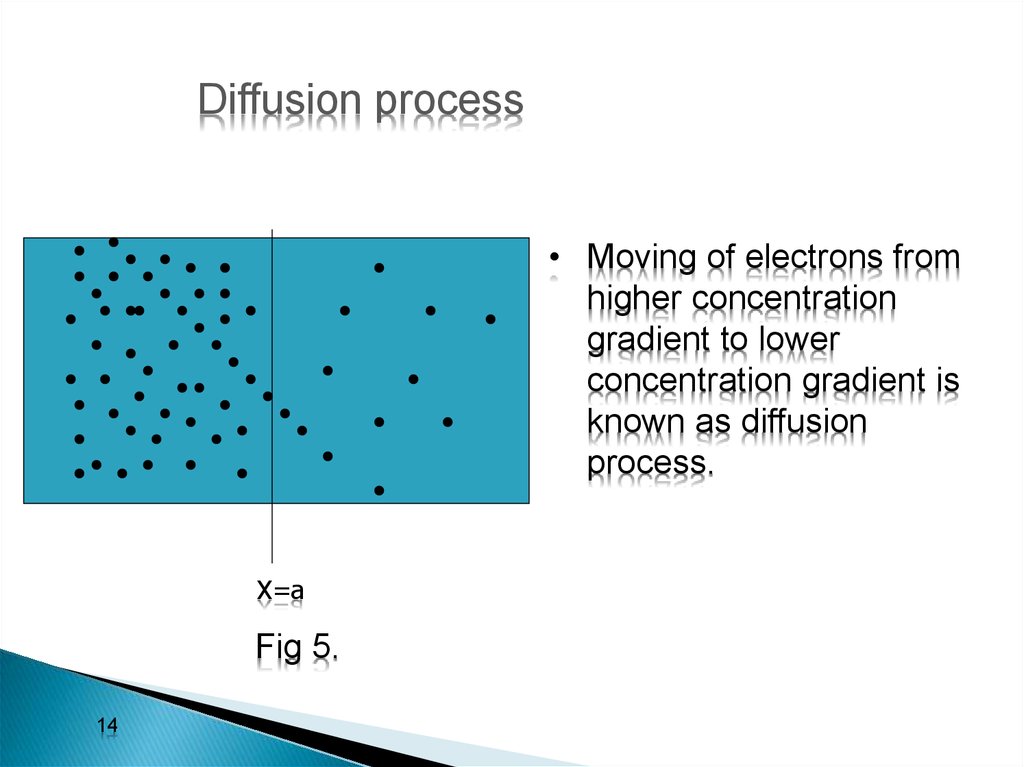
14.
Diffusion process• Moving of electrons from
higher concentration
gradient to lower
concentration gradient is
known as diffusion
process.
X=a
Fig 5.
14
15. P and N type Semiconductors
Acceptor ionP
Donor ion
-
-
-
-
+
+
+
+
-
-
-
-
+
+
+
+
-
-
+
+
Minority electron
Majority holes
Majority electrons
Fig 1.
15
N
+
Minority hole
16. Formation of pn diode
Depletion RegionP
N
-
-
-
-
+
+
+
+
-
-
-
-
+
+
+
+
-
-
+
+
-
+
Fig 2.
Potential barrier
16
Vb
17. Semiconductor diodes
Fig. 1 Diode variants17
Visual - 1