Similar presentations:
Топологии импульсных преобразователей
1. Switching Power Supplies A to Z Basic Switcher Architectures
Thanks to John Bittner2. Voltage Mode Buck Regulator Basic Architecture
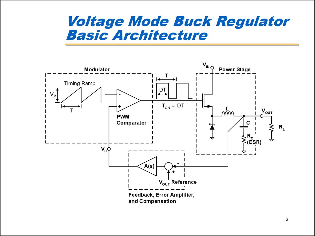
VINModulator
Power Stage
T
Timing Ramp
VP
DT
+
TON = DT
T
PWM
Comparator
L
VOUT
C
RL
RC
(ESR)
VC
-
A(s)
+
VOUT Reference
Feedback, Error Amplifier,
and Compensation
2
3. Feedback, Error Amplifier, and Compensation – Two Types
Gm Amp:VOUT
RF1
-
VC
Gm
RF2
+
Gain is a function of the feedback ratio, so
regulator loop gain increases inversely with
VOUT. Gain is also affected by changes in A(s).
+
Z(s)
-
VREF
Op-Amp:
VOUT
Z2(s)
VC
R F2
Gm Z(s)
VOUT
R F1 R F2
V
REF A(s) A(s) Gm Z(s)
VOUT
Z1(s)*
VC
Z (s)
2
VOUT
Z 1 (s)
Loop gain is independent of op-amp’s open
loop gain and the feedback ratio.
VC
RF2
+
+
-
VREF
* Z 1 (s) R F1 at DC:
R R F2
VOUT (DC) VREF F1
R F2
3
4. Voltage Mode Buck Regulator Loop Gain
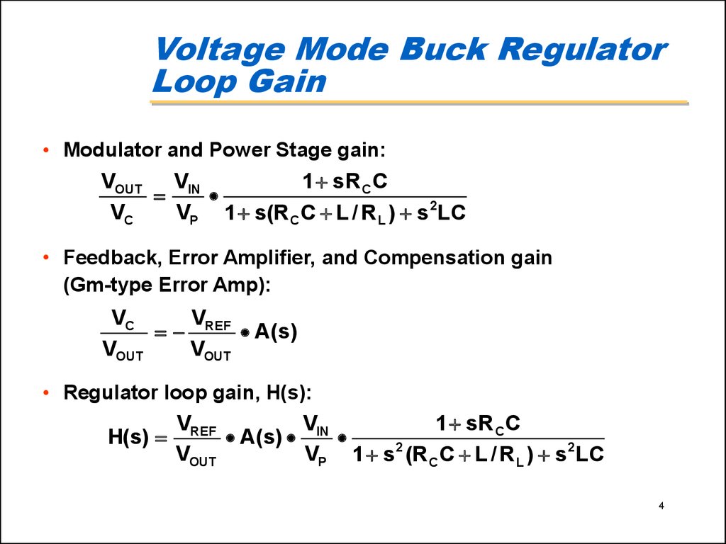
• Modulator and Power Stage gain:VOUT
V
1 sR C C
IN
VC
VP 1 s(R C C L / R L ) s 2LC
• Feedback, Error Amplifier, and Compensation gain
(Gm-type Error Amp):
VC
V
REF A(s)
VOUT
VOUT
• Regulator loop gain, H(s):
VREF
VIN
1 sR C C
H(s)
A ( s)
VOUT
VP 1 s 2 (R C C L / R L ) s 2LC
4
5. Voltage-Mode Buck Regulator Frequency Response
f (deg)0
Gain (dB)
-90o
1
2p LC
Mid-band
gain
20dB
fM
-180o
1
2pCRC
-40dB/dec
0
1k
10k
f0
-20dB/dec
100k
freq (Hz)
6. Current Mode Buck Regulator Basic Architecture
VINModulator and Power Stage
Current-Sense
Amplifier
Ai
+
+
Se
RS
-
Corrective Ramp
PWM
Comparator
-
DT
+
Sn
+
T
L
DT
VOUT
C
T
RL
RC
(ESR)
VC
A(s)
+
VOUT Reference
Feedback, Error Amplifier,
and Compensation
6
7. Current Mode Buck Regulator Loop Gain
• Gain of Modulator and Power Stage:VOUT R L
VC
Ri
1 sR C C
1
2
RLT
s
s
s
1
1
(mCD 0.5)
1
2
P
L
NQ P N
R i Ai R S
mC 1
P
Se
Sn
1
D' 1 D
Se = corrective ramp slope
Sn = positive slope current-sense waveform
1
T
(mCD 0.5)
CRL LC
fSW p
N 2p
2
T
QP
1
p(mCD 0.5)
7
8. Current Mode Buck Regulator Loop Gain
• Feedback, Error Amplifier, and Compensation gain(Gm-type Error Amp):
VC
V
REF A(s)
VOUT
VOUT
A(s) Gm Z(s)
• Regulator loop gain:
H(s)
VREF
R
1 sR C C
A ( s) L K
Fh(s)
s
VOUT
Ri
1
P
K
1
R T
1 L SW (mCD' 0.5)
L
1
Fh(s)
1
s
N Q P
s2
N
2
8
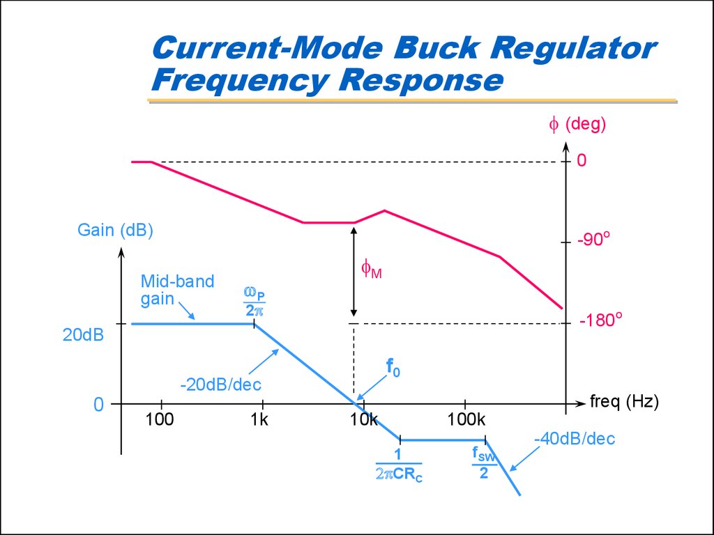
9. Current-Mode Buck Regulator Frequency Response
f (deg)0
Gain (dB)
-90o
Mid-band
gain
P
fM
2p
-180o
20dB
f0
-20dB/dec
0
freq (Hz)
100
1k
10k
1
2pCRC
100k
fSW
2
-40dB/dec
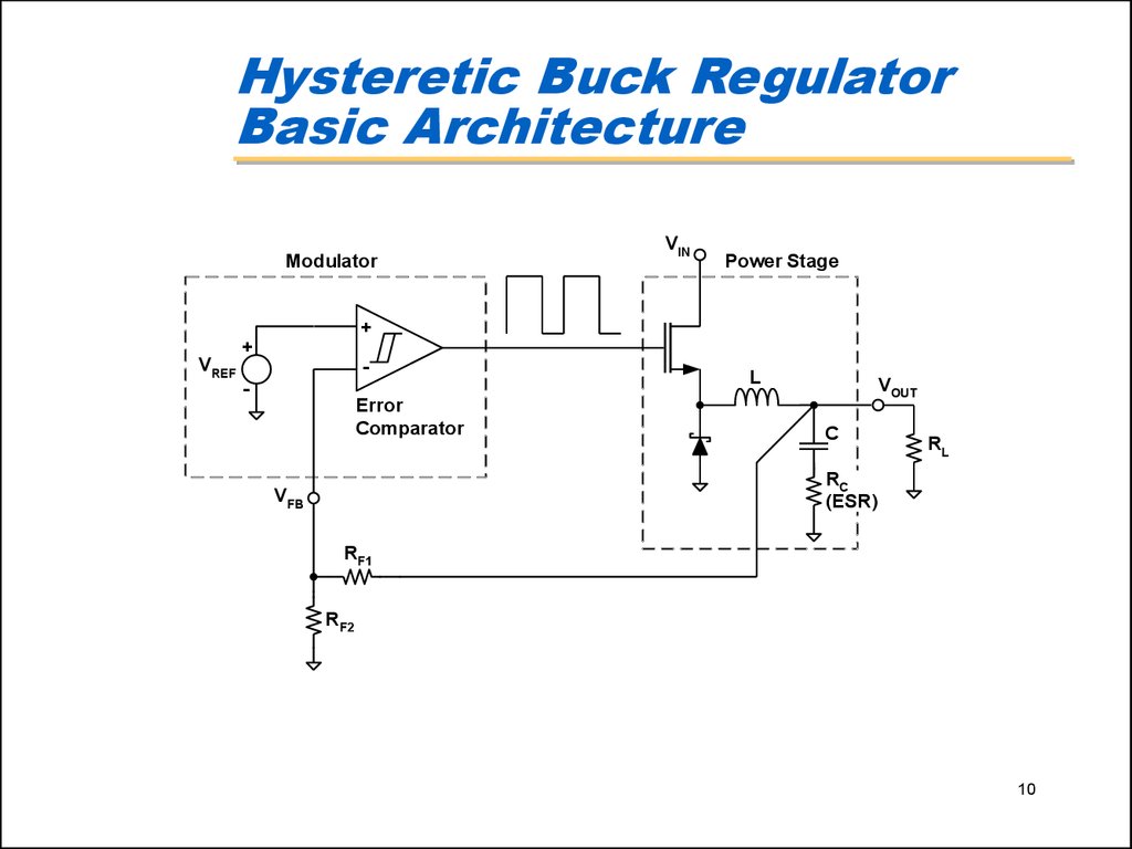
10. Hysteretic Buck Regulator Basic Architecture
ModulatorVIN
Power Stage
+
+
VREF
-
Error
Comparator
L
VOUT
C
RL
RC
(ESR)
VFB
RF1
RF2
10
11. Hysteretic Buck Regulator Switching Waveforms
VSWVIN
tON
tON and tOFF are functions
of VIN, VOUT, L, ESR, ESL,
VHYS*(RF1+RF2)/RF2, and td
tOFF
-0.6V
IL
IL
IOUT
IL
VOUT
VIN VOUT
V
t ON OUT t OFF
L
L
td
VOUT
VOUT(DC)
VHYS
R F1 R F2
VHYS 15mV
R F2
td
11
12. Calculating Hysteretic Regulator Switching Frequency
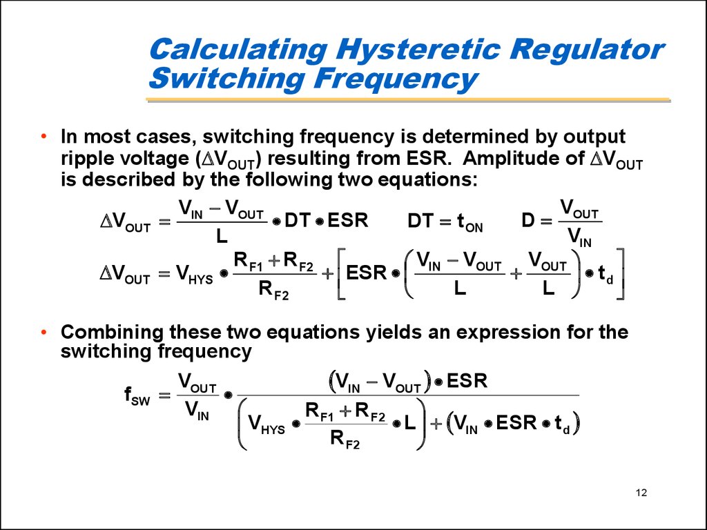
• In most cases, switching frequency is determined by outputripple voltage ( VOUT) resulting from ESR. Amplitude of VOUT
is described by the following two equations:
V
V VOUT
D OUT
VOUT IN
DT ESR
DT t ON
VIN
L
R R F2
V VOUT VOUT
VOUT VHYS F1
ESR IN
td
R F2
L
L
• Combining these two equations yields an expression for the
switching frequency
VIN VOUT ESR
V
fSW OUT
VIN
R R F2
VHYS F1
L VIN ESR t d
R F2
12
13. Compensating for excessive ESL in output capacitor
VIN4.5V to 35V
CIN
22uF
L1
22uH
Q1
VOUT
3.3V
C1
47nF
RADJ
CADJ
COUT
100uF
R3
18k
PGATE
ADJ
VIN
R1
33k
ISENSE
FB
R2
20k
C2
33nF
COUT has excessive ESL, so VOUT has large voltage steps that result in erratic
switching. C2 filters-out ESL voltage step at FB pin. C1, C3 and R3 generate
triangle waveform that determines the switching frequency.
13
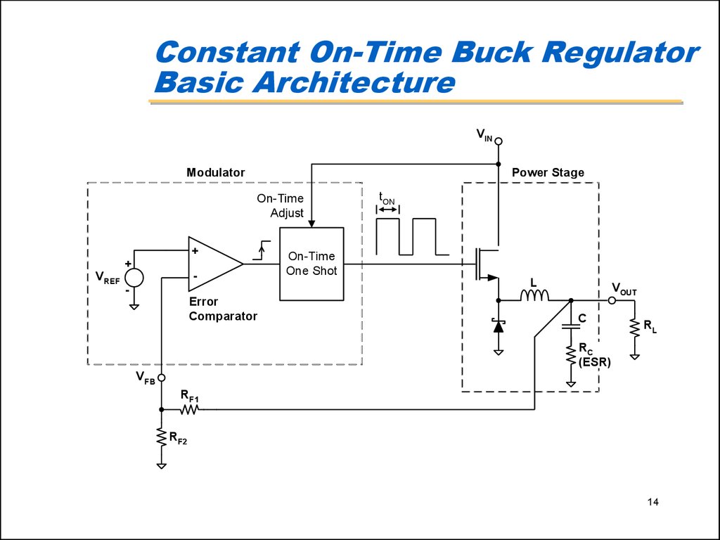
14. Constant On-Time Buck Regulator Basic Architecture
VINModulator
Power Stage
On-Time
Adjust
+
+
-
VREF
Error
Comparator
tON
On-Time
One Shot
L
VOUT
C
RL
RC
(ESR)
VFB
RF1
RF2
14
15. Constant On-time Buck Regulator Switching Waveforms
VSWtON is set by a one-shot
timer that decreases tON
as VIN increases.
VIN
tON
tOFF
tOFF is a function of VIN,
VOUT, and tON
-0.6V
IL
IL
IOUT
IL
VOUT
VOUT
VOUT(DC)
VREF
R F1 R F2
R F2
VIN VOUT
V
t ON OUT t OFF
L
L
td
15
16. Calculating Constant 0n-Time Regulator Switching Frequency
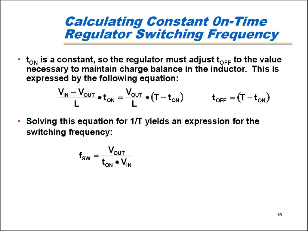
• tON is a constant, so the regulator must adjust tOFF to the valuenecessary to maintain charge balance in the inductor. This is
expressed by the following equation:
VIN VOUT
V
t ON OUT T t ON
L
L
t OFF T t ON
• Solving this equation for 1/T yields an expression for the
switching frequency:
fSW
VOUT
t ON VIN
16






 physics
 english


