


 informatics
Similar presentations:


CMOS Processes
1. CMOS Processes
Hong Xiao, Ph. D.www2.austin.cc.tx.us/HongXiao/Boo
k.htm
1
2. 1990’s Technology
• Driving force: digital logic electronics– PC, telecommunication, and internet.
• Feature size: from 0.8 mm to 0.18 mm
• Wafer size: from 150 mm to 300 mm
Hong Xiao, Ph. D.
www2.austin.cc.tx.us/HongXiao/Boo
k.htm
2
3. 1990’s CMOS Technology
• Epitaxy silicon• Shallow trench isolation
• The sidewall spacer for LDD and salicide
• Polycide gates and local interconnections
reduce resistance and improve device speed
– Tungsten silicide and titanium silicide.
Hong Xiao, Ph. D.
www2.austin.cc.tx.us/HongXiao/Boo
k.htm
3
4. 1990’s CMOS Technology
• Photolithography– G-line, I-line (365 nm), and DUV 248 nm
– Positive photoresist
– Steppers replaced projection printer
– Track-stepper integrated systems
• Plasma etches for patterned etch
• Wet etches for blanket film stripping
Hong Xiao, Ph. D.
www2.austin.cc.tx.us/HongXiao/Boo
k.htm
4
5. 1990’s CMOS Technology
• Vertical furnaces– smaller footprints, better contamination control.
• RTP systems
– post-implantation annealing
– silicide formation,
– faster, better process and thermal budget control.
• DC magnetron sputtering replaced evaporation
Hong Xiao, Ph. D.
www2.austin.cc.tx.us/HongXiao/Boo
k.htm
5
6. 1990’s CMOS Technology
• Multi-layer metal interconnection• W CVD and CMP (or etch back) to form plugs
• Ti and TiN barrier/adhesion layer for W
• Ti welding layer for Al-Cu to reduce contact
resistance
• TiN ARC
Hong Xiao, Ph. D.
www2.austin.cc.tx.us/HongXiao/Boo
k.htm
6
7. 1990’s CMOS Technology
• BPSG was popularly used as PMD.• DCVD: PE-TEOS and O3-TEOS
– STI, sidewall spacer, PMD, and IMD
• DCVD: PE-silane
– PMD barrier nitride, dielectric ARC, and PD nitride
• Tungsten CMP to form plug
• Dielectric CMP for planarization
Hong Xiao, Ph. D.
www2.austin.cc.tx.us/HongXiao/Boo
k.htm
7
8. 1990’s CMOS Technology
• Cluster tools became very popular• Single wafer processing systems improve
wafer-to-wafer uniformity control
• Batch systems is still commonly employed
in many non-critical processes for their high
throughput.
Hong Xiao, Ph. D.
www2.austin.cc.tx.us/HongXiao/Boo
k.htm
8
9. Epitaxy Deposition
P-EpiHong Xiao, Ph. D.
P-Wafer
www2.austin.cc.tx.us/HongXiao/Boo
k.htm
9
10. Mask 1: N-well
Hong Xiao, Ph. D.www2.austin.cc.tx.us/HongXiao/Boo
k.htm
10
11. N-well Implantation
Phosphorus IonsPhotoresist
N-Well
P-Epi
Hong Xiao, Ph. D.
P-Wafer
www2.austin.cc.tx.us/HongXiao/Boo
k.htm
11
12.
Mask 2: P-wellHong Xiao, Ph. D.
www2.austin.cc.tx.us/HongXiao/Boo
k.htm
12
13. P-well Implantation
Boron IonsPhotoresist
P-Well
N-Well
P-Epi
Hong Xiao, Ph. D.
P-Wafer
www2.austin.cc.tx.us/HongXiao/Boo
k.htm
13
14. Strip PR, Strip Nitride/Pad Oxide
P-WellP-Epi
Hong Xiao, Ph. D.
N-Well
P-Wafer
www2.austin.cc.tx.us/HongXiao/Boo
k.htm
14
15. Pad Oxidation, LPCVD Nitride
NitrideP-Well
P-Epi
Hong Xiao, Ph. D.
N-Well
P-Wafer
www2.austin.cc.tx.us/HongXiao/Boo
k.htm
15
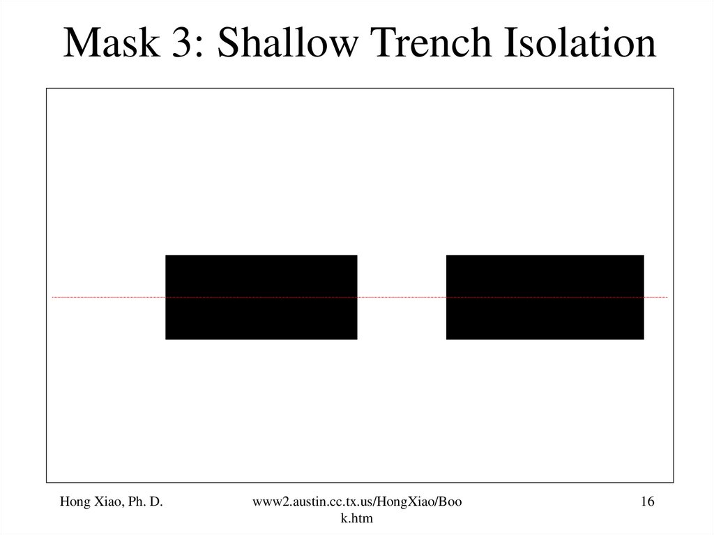
16.
Mask 3: Shallow Trench IsolationHong Xiao, Ph. D.
www2.austin.cc.tx.us/HongXiao/Boo
k.htm
16
17. Etch Nitride, Pad Oxide and Silicon
NitrideNitride
P-Well
P-Epi
Hong Xiao, Ph. D.
N-Well
P-Wafer
www2.austin.cc.tx.us/HongXiao/Boo
k.htm
17
18. HDP-CVD USG Trench Fill
USGNitride
Nitride
USG
P-Well
P-Epi
Hong Xiao, Ph. D.
N-Well
P-Wafer
www2.austin.cc.tx.us/HongXiao/Boo
k.htm
18
19. CMP USG, Stop on Nitride
NitrideNitride
USG
P-Well
P-Epi
Hong Xiao, Ph. D.
N-Well
P-Wafer
www2.austin.cc.tx.us/HongXiao/Boo
k.htm
19
20. Strip Nitride and Pad Oxide, Clean
USGSTI
P-Well
P-Epi
Hong Xiao, Ph. D.
N-Well
P-Wafer
www2.austin.cc.tx.us/HongXiao/Boo
k.htm
20
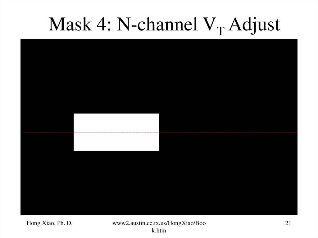
21.
Mask 4: N-channel VT AdjustHong Xiao, Ph. D.
www2.austin.cc.tx.us/HongXiao/Boo
k.htm
21
22.
Phosphorus IonsPhotoresist
USG
STI
P-Well
P-Epi
Hong Xiao, Ph. D.
N-Well
P-Wafer
www2.austin.cc.tx.us/HongXiao/Boo
k.htm
22
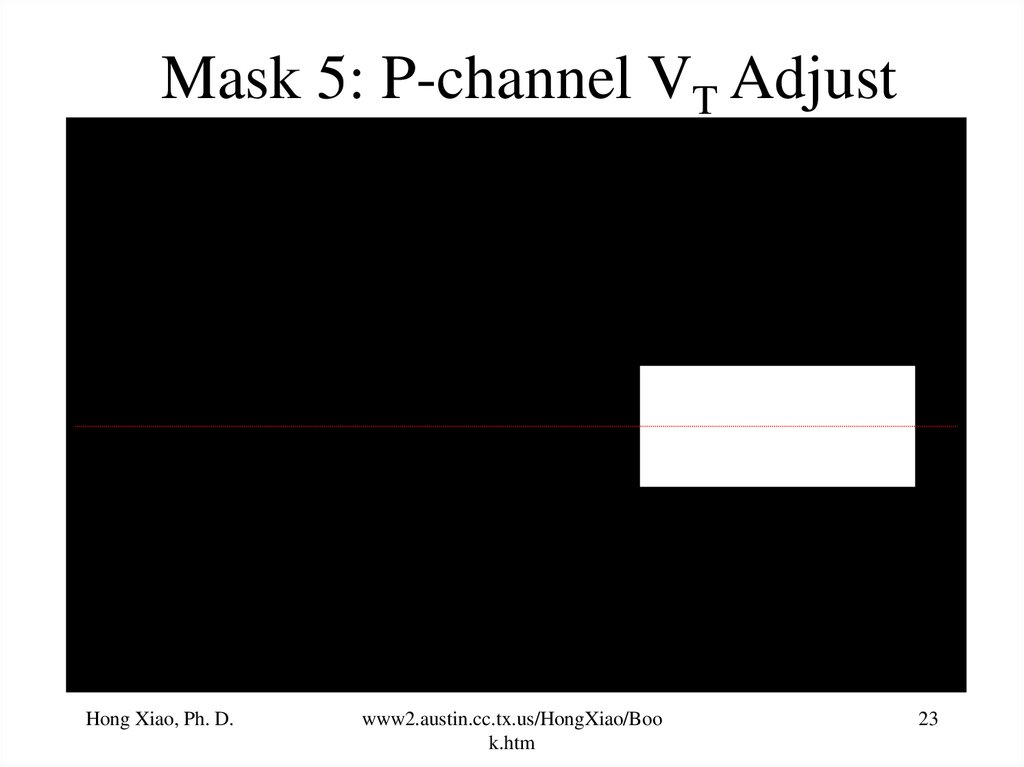
23.
Mask 5: P-channel VT AdjustHong Xiao, Ph. D.
www2.austin.cc.tx.us/HongXiao/Boo
k.htm
23
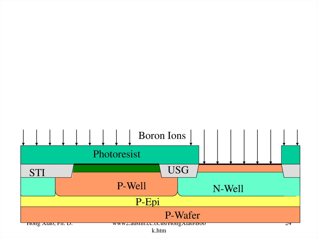
24.
Boron IonsPhotoresist
USG
STI
P-Well
P-Epi
Hong Xiao, Ph. D.
N-Well
P-Wafer
www2.austin.cc.tx.us/HongXiao/Boo
k.htm
24
25. Gate Oxidation, LPCVD Polysilicon
PolysiliconUSG
STI
P-Well
P-Epi
Hong Xiao, Ph. D.
N-Well
P-Wafer
www2.austin.cc.tx.us/HongXiao/Boo
k.htm
25
26.
Mask 6: Gate & Local InterconnectionHong Xiao, Ph. D.
www2.austin.cc.tx.us/HongXiao/Boo
k.htm
26
27. Etch Polysilicon
Gate OxideSTI
Hong Xiao, Ph. D.
Photoresist
Polysilicon gate
USG
P-Well
N-Well
P-Epi
P-Wafer
www2.austin.cc.tx.us/HongXiao/Boo
k.htm
27
28.
Mask 7: N-channel LDDHong Xiao, Ph. D.
www2.austin.cc.tx.us/HongXiao/Boo
k.htm
28
29. N-channel LDD Implantation, Arsenic
Arsenic IonsPhotoresist
USG
STI
P-Well
P-Epi
Hong Xiao, Ph. D.
N-Well
P-Wafer
www2.austin.cc.tx.us/HongXiao/Boo
k.htm
29
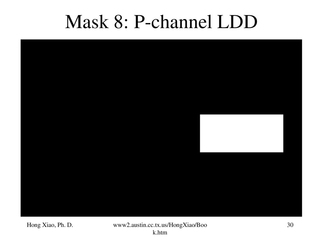
30.
Mask 8: P-channel LDDHong Xiao, Ph. D.
www2.austin.cc.tx.us/HongXiao/Boo
k.htm
30
31. P-channel LDD Implantation, BF2+
+P-channel LDD Implantation, BF2
BF2+ Ions
Photoresist
USG
STI
P-Well
P-Epi
Hong Xiao, Ph. D.
N-Well
P-Wafer
www2.austin.cc.tx.us/HongXiao/Boo
k.htm
31
32. Sidewall Spacer
Polysilicon gaten-LDD
Gate oxide
Hong Xiao, Ph. D.
n-LDD
Sidewall
Spacer
Polysilicon gate
n-LDD
Gate oxide
www2.austin.cc.tx.us/HongXiao/Boo
k.htm
Sidewall
Spacer
n-LDD
32
33.
Mask 9: N-channel Source/DrainHong Xiao, Ph. D.
www2.austin.cc.tx.us/HongXiao/Boo
k.htm
33
34. N-channel Source/Drain Implantation
Phosphorus IonsPhotoresist
STI
n+
n+
USG
P-Well
P-Epi
Hong Xiao, Ph. D.
p-
p-
N-Well
P-Wafer
www2.austin.cc.tx.us/HongXiao/Boo
k.htm
34
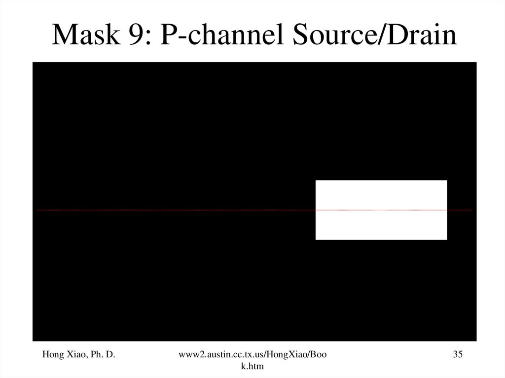
35.
Mask 9: P-channel Source/DrainHong Xiao, Ph. D.
www2.austin.cc.tx.us/HongXiao/Boo
k.htm
35
36. P-channel Source/Drain Implantation
Boron IonsPhotoresist
STI
Hong Xiao, Ph. D.
n+
n+
USG
p+
P-Well
N-Well
P-Epi
P-Wafer
www2.austin.cc.tx.us/HongXiao/Boo
k.htm
p+
36
37. Titanium Salicide Process
ArAr +
+
Sidewall
spacer
n-
n+
Polysilicon gate
Gate oxide
Ti
Sidewall
spacer
Polysilicon gate
n-
nn+
n+
Gate oxide
nn+
Ti
TiSi2
Polysilicon gate
nn+
TiSi2
Gate oxide
Hong Xiao, Ph. D.
TiSi2
Polysilicon gate
n-
nn+
TiSi2
n+
www2.austin.cc.tx.us/HongXiao/Boo
k.htm
Gate oxide
n-
n+
37
38. Titanium Self-aligned silicide Process
Titanium DepositionSTI
Sidewall Spacer
Silicon
Titanium
RTP Silicide Alloying
Silicon
Strip Unreact Titanium
Polysilicon
Hong Xiao, Ph. D.
Titanium Silicide
Silicon
www2.austin.cc.tx.us/HongXiao/Boo
Gate
Oxide
k.htm
38
39. BPSG Deposition and Reflow
BPSGSTI
n+
n+
n+
USG
p+
p+
USG
p+
p+
BPSG
STI
Hong Xiao, Ph. D.
n+
www2.austin.cc.tx.us/HongXiao/Boo
k.htm
39
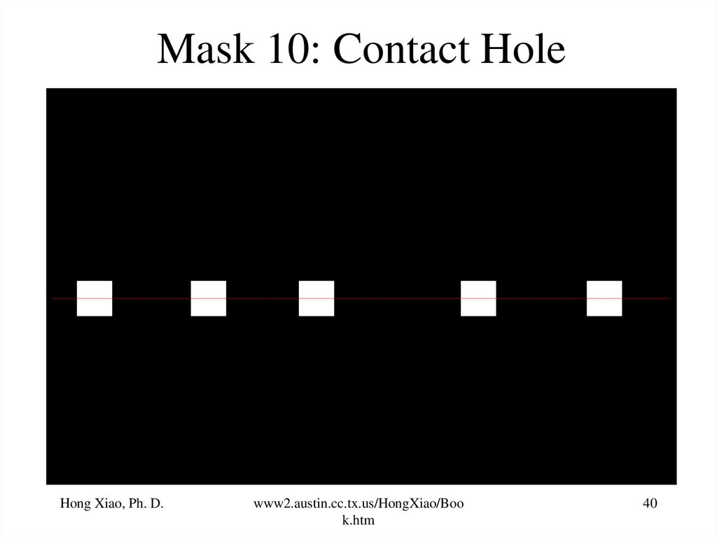
40.
Mask 10: Contact HoleHong Xiao, Ph. D.
www2.austin.cc.tx.us/HongXiao/Boo
k.htm
40
41. Contact Hole Etch, BPSG Etch
BPSGSTI
Hong Xiao, Ph. D.
n+
n+
p+
USG
P-Well
N-Well
P-Epi
P-Wafer
www2.austin.cc.tx.us/HongXiao/Boo
k.htm
p+
41
42. Contact Hole Etch, BPSG Etch
Titanium/Titanium NitrideTungsten
BPSG
STI
Hong Xiao, Ph. D.
n+
n+
p+
USG
P-Well
N-Well
P-Epi
P-Wafer
www2.austin.cc.tx.us/HongXiao/Boo
k.htm
p+
42
43. Contact Hole Etch, BPSG Etch
Titanium/Titanium NitrideTiN ARC
Titanium
Aluminum Copper Alloy
W BPSG
STI
Hong Xiao, Ph. D.
n+
n+
p+
USG
P-Well
N-Well
P-Epi
P-Wafer
www2.austin.cc.tx.us/HongXiao/Boo
k.htm
p+
43
44. Mask 11: Metal 1 Interconnect
Hong Xiao, Ph. D.www2.austin.cc.tx.us/HongXiao/Boo
k.htm
44
45. Metal Etch
Titanium/Titanium NitrideTiN ARC
Titanium
Al-Cu Alloy
W BPSG
STI
Hong Xiao, Ph. D.
n+
n+
p+
USG
P-Well
N-Well
P-Epi
P-Wafer
www2.austin.cc.tx.us/HongXiao/Boo
k.htm
p+
45
46. PE-TEOS USG Dep/Etch/Dep/CMP
IMD 1USG Dep/Etch/Dep/CMP
Al-Cu Alloy
W BPSG
STI
Hong Xiao, Ph. D.
n+
n+
USG
P-Well
P-Epi
P-Wafer
www2.austin.cc.tx.us/HongXiao/Boo
k.htm
p+
p+
N-Well
46
47. Mask 12: Via 1
Hong Xiao, Ph. D.www2.austin.cc.tx.us/HongXiao/Boo
k.htm
47
48. Via Etch, Etch USG
IMD 1USG
Al-Cu Alloy
W BPSG
STI
Hong Xiao, Ph. D.
n+
n+
USG
P-Well
P-Epi
P-Wafer
www2.austin.cc.tx.us/HongXiao/Boo
k.htm
p+
p+
N-Well
48
49. Via Etch, Etch USG
Metal 2IMD 1
Al-Cu Alloy
USG
M1
Al-Cu Alloy
W BPSG
STI
Hong Xiao, Ph. D.
n+
n+
USG
P-Well
P-Epi
P-Wafer
www2.austin.cc.tx.us/HongXiao/Boo
k.htm
p+
p+
N-Well
49
50. Mask 13: Metal 2 Interconnect
Hong Xiao, Ph. D.www2.austin.cc.tx.us/HongXiao/Boo
k.htm
50
51. Etch Metal 2
M2IMD 1
Al•Cu
USG
M1
Al•Cu Alloy
W BPSG
STI
Hong Xiao, Ph. D.
n+
n+
USG
P-Well
P-Epi
P-Wafer
www2.austin.cc.tx.us/HongXiao/Boo
k.htm
p+
p+
N-Well
51
52. USG Dep/Etch/Dep/CMP
IMD 2USG
M2
IMD 1
Al•Cu
USG
M1
Al•Cu Alloy
W BPSG
STI
Hong Xiao, Ph. D.
n+
n+
USG
P-Well
P-Epi
P-Wafer
www2.austin.cc.tx.us/HongXiao/Boo
k.htm
p+
p+
N-Well
52
53. Mask 14: Via 2
Hong Xiao, Ph. D.www2.austin.cc.tx.us/HongXiao/Boo
k.htm
53
54. Via 2 Etch, Etch USG
IMD 2USG
M2
IMD 1
Al•Cu
USG
M1
Al•Cu Alloy
W BPSG
STI
Hong Xiao, Ph. D.
n+
n+
P-Well
USG
www2.austin.cc.tx.us/HongXiao/Boo
k.htm
p+
N-Well
p+
54
55. Metallization of Metal 3
Metal 3IMD 2
USG
M2
IMD 1
Al•Cu Alloy
W
Al•Cu
USG
M1
Al•Cu Alloy
W BPSG
STI
Hong Xiao, Ph. D.
n+
n+
P-Well
USG
www2.austin.cc.tx.us/HongXiao/Boo
k.htm
p+
N-Well
p+
55
56. Mask 15: Metal 3 Interconnects
Hong Xiao, Ph. D.www2.austin.cc.tx.us/HongXiao/Boo
k.htm
56
57. Metal Etch, PR Strip and Metal Anneal
Metal 3IMD 2
USG
W
Al•Cu
M2
IMD 1
Al•Cu Alloy
USG
Al•Cu Alloy
M1
W BPSG
STI
Hong Xiao, Ph. D.
n+
n+
P-Well
USG
www2.austin.cc.tx.us/HongXiao/Boo
k.htm
p+
N-Well
p+
57
58. PE-TEOS USG Dep/Etch/Dep/CMP
IMD 3USG
Metal 3
IMD 2
USG
M2
IMD 1
Hong Xiao, Ph. D.
Al•Cu Alloy
W
Al•Cu
USG
M1
Al•Cu Alloy
www2.austin.cc.tx.us/HongXiao/Boo
k.htm
58
59. Mask 16: Via 3
Hong Xiao, Ph. D.www2.austin.cc.tx.us/HongXiao/Boo
k.htm
59
60. Via 3 Etch and PR Strip
IMD 3USG
Metal 3
IMD 2
USG
Hong Xiao, Ph. D.
W
Al•Cu
M2
IMD 1
Al•Cu Alloy
USG
M1
Al•Cu Alloy
www2.austin.cc.tx.us/HongXiao/Boo
k.htm
60
61. Metal 4 Deposition
Al•CuMetal 4
IMD 3
USG
Metal 3
IMD 2
USG
M2
IMD 1
Hong Xiao, Ph. D.
Al•Cu Alloy
W
Al•Cu
USG
M1
Al•Cu Alloy
www2.austin.cc.tx.us/HongXiao/Boo
k.htm
61
62. Mask 17: Metal 4 Interconnects
Hong Xiao, Ph. D.www2.austin.cc.tx.us/HongXiao/Boo
k.htm
62
63. Etch Metal 4
Al•Cu AlloyAl•Cu
Metal 4
IMD 3
USG
Metal 3
Hong Xiao, Ph. D.
Al•Cu Alloy
www2.austin.cc.tx.us/HongXiao/Boo
k.htm
63
64. Passivation Dielectric Deposition
Silicon NitrideUSG
Al•Cu Alloy
Al•Cu
Metal 4
IMD 3
USG
Metal 3
Hong Xiao, Ph. D.
Al•Cu Alloy
www2.austin.cc.tx.us/HongXiao/Boo
k.htm
64
65. Mask 18: Bonding Pad
Hong Xiao, Ph. D.www2.austin.cc.tx.us/HongXiao/Boo
k.htm
65
66. Etch Bonding Pad, Strip PR
Silicon NitrideUSG
Al•Cu Alloy
Al•Cu
Metal 4
IMD 3
USG
Metal 3
Hong Xiao, Ph. D.
Al•Cu Alloy
www2.austin.cc.tx.us/HongXiao/Boo
k.htm
66
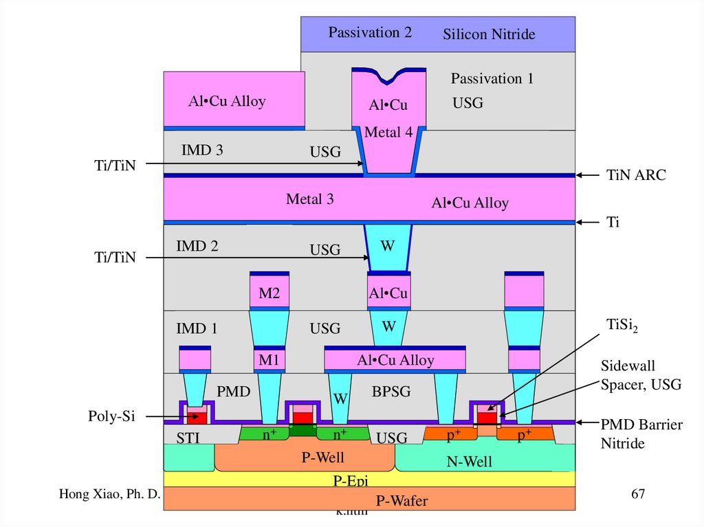
67.
Passivation 2Silicon Nitride
Passivation 1
Al•Cu Alloy
USG
Al•Cu
Metal 4
Ti/TiN
IMD33
IMD
USG
TiN ARC
Metal 3
Al•Cu Alloy
Ti
Ti/TiN
IMD 2
W
USG
M2
IMD 1
Al•Cu
M1
PMD
TiSi2
W
USG
Al•Cu Alloy
W
Sidewall
Spacer, USG
BPSG
Poly-Si
STI
Hong Xiao, Ph. D.
n+
n+
p+
USG
P-Well
N-Well
P-Epi
www2.austin.cc.tx.us/HongXiao/Boo
P-Wafer
k.htm
p+
PMD Barrier
Nitride
67
68. Lead-Tin Alloy Coating
Lead-tin alloyNitride
PSG
Copper 5
SOD
SOD
Hong Xiao, Ph. D.
www2.austin.cc.tx.us/HongXiao/Boo
k.htm
68
69. PR Coating, A&E, PEB, and Develop
PR Coating, A&E, PEB, and DevelopPhotoresist
Lead-tin alloy
Nitride
PSG
Copper 5
SOD
SOD
Hong Xiao, Ph. D.
www2.austin.cc.tx.us/HongXiao/Boo
k.htm
69
70. Metal Etch
PhotoresistLead-tin alloy
Nitride
PSG
Copper 5
SOD
SOD
Hong Xiao, Ph. D.
www2.austin.cc.tx.us/HongXiao/Boo
k.htm
70
71. Strip Photoresist
Lead-tin alloyNitride
PSG
Copper 5
SOD
SOD
Hong Xiao, Ph. D.
www2.austin.cc.tx.us/HongXiao/Boo
k.htm
71
72. Lead-Tin Alloy Reflow
Lead-tin alloyNitride
PSG
Copper 5
SOD
SOD
Hong Xiao, Ph. D.
www2.austin.cc.tx.us/HongXiao/Boo
k.htm
72
73.
Cr, Cu, andAu liners
Lead-tin alloy
Nitride
SiN seal
layer
PSG
Copper 5
SOD
SOD
Copper 4
SOD
SiC etch
stop layers
Ta/TaN
barrier layer
SOD
Cu 3
SOD
Cu 3
SOD
Copper 2
SOD
SiC seal layer
SOD
PE-TEOS cap
Cu 1
Cu 1 SOD
CoSi2
Poly Si gate
Hong Xiao, Ph. D.
Cu 1
Cu 1
SOD
W
SiC seal layer
PSG
Tungsten
n+
n+ USG p+
STI www2.austin.cc.tx.us/HongXiao/Boo
P-well
N-well
Buried SiO 2 k.htm
P-wafer
p+
USG
SiN barrier
layer
73