


 electronics
Similar presentations:


. Junction field-effect transistor (JFET)")


Introduction to Electronics (lecture 1)
1.
Introduction to Electronics.Semiconductors.
Presented by
Senior-lecturer
MСs of Engineering and Technology in Electrical Engineering
2.
Brief HistoryThe year 1899 is one possibility. During that year, J. J. Thomson, at the University of
Cambridge in England, discovered the electron.
Two important developments at the beginning of the 20th century made people
interested in electronics:
• The first was in 1901, when Guglielmo Marconi sent a message across the Atlantic Ocean
using wireless telegraphy. Today we call wireless communication radio.
• The second development came in 1906, when Lee De Forest invented the audion vacuum
tube. The term audion related to its first use, to make sounds (“audio”) louder. It was not
long before the wireless inventors used the vacuum tube to improve their equipment.
Another development in 1906 is worth mentioning. Greenleaf W. Pickard used the first
crystal radio detector. This great improvement helped make radio and electronics more
popular. It also suggested the use of semiconductors (crystals) as materials with future
promise for the new field of radio and electronics.
3.
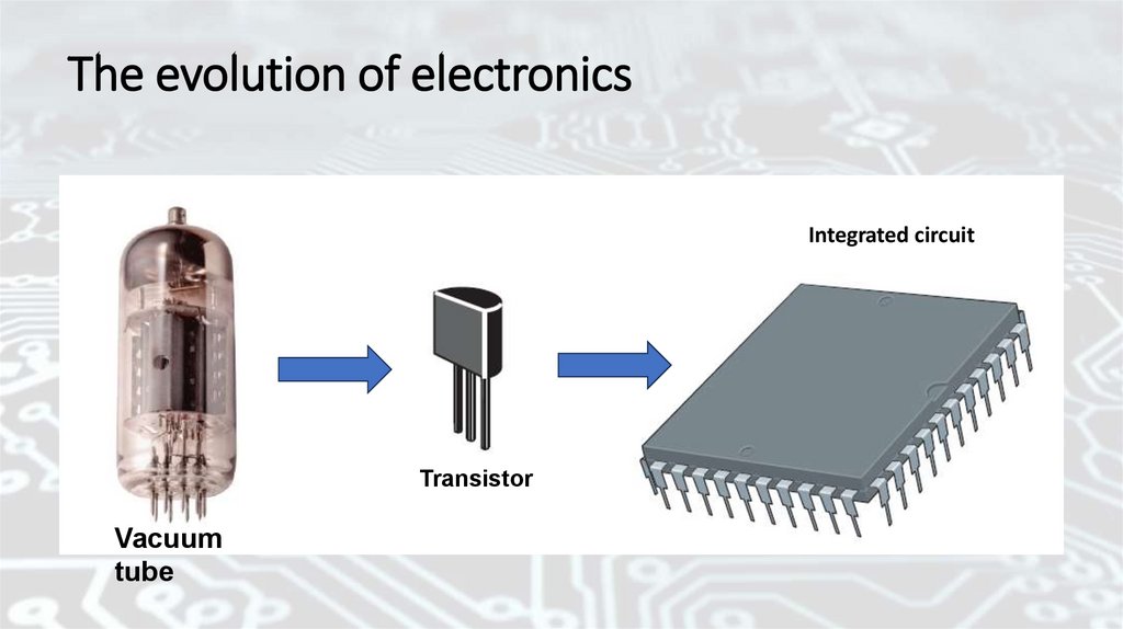
The evolution of electronicsIntegrated circuit
Transistor
Vacuum
tube
4.
Radio, television and computer• Commercial radio was born in Pittsburgh, Pennsylvania, at
station KDKA in 1920;
• Commercial television began around 1946. In 1947 several
hundred thousand home radio receivers were manufactured
and sold;
• The ENIAC was formally dedicated at the Moore School of
Electrical Engineering of the University of Pennsylvania on
February 15, 1946. It was the world’s first electronic digital
computer.
5.
TransistorThe breakthrough came in 1947. Three
scientists working with Bell Laboratories made
the first working transistor. This was such a major
contribution to science and technology that the
three men—John Bardeen, Walter H. Brattain,
and William B. Shockley—were awarded the
Nobel Prize.
6.
Integrated circuitSolid-state circuits were small, efficient, and more
reliable. But the scientists and engineers still were not
satisfied. Work done by Jack Kilby of Texas Instruments
led to the development of the integrated circuit in
1958. Robert Noyce, working at Fairchild, developed a
similar project. The two men shared a Nobel Prize in
Physics for inventing the integrated circuit.
7.
MicroprocessorIn 1971 Intel Corporation in California announced one of
the most sophisticated of all integrated circuits—the
microprocessor. A microprocessor is most of the circuitry of a
computer reduced to a single integrated circuit.
Microprocessors, some containing the equivalent of billions of
transistors, have provided billions of dollars worth of growth
for the electronics industry and have opened up entire new
areas of applications.
The Intel 4004 contained 2,300 transistors, and today a
Xeon processor has more than 6 billion. The 4004 had
features as small as 10 micrometers (μm), and today the
feature size is shrinking toward 10 nanometers (nm).
8.
Digital or AnalogElectronics can be divided is into digital or analog.
A digital electronic device or circuit will recognize or
produce an output of only several limited states. For example,
most digital circuits will respond to only two input conditions:
low or high. Digital circuits may also be called binary since
they are based on a number system with only two digits: 0
and 1.
An analog circuit can respond to or produce an output for
an infinite number of states.
9.
Voltage of Digital and Analog signalsAn analog input or output might vary between 0 and 10 volts
(V). Its actual value could be 1.5, 2.8, or even 7.653 V. In theory,
an infinite number of voltages are possible. On the other hand,
the typical digital circuit recognizes inputs ranging from 0 to 0.4 V
as low (binary 0) and those ranging from 2.0 to 5 V as high
(binary 1). A digital circuit does not respond any differently for an
input of 2 V than it does for one at 4 V. Both of these voltages are
in the high range. Input voltages between 0.4 and 2.0 V are not
allowed in digital systems because they cause an output that is
unpredictable.
10.
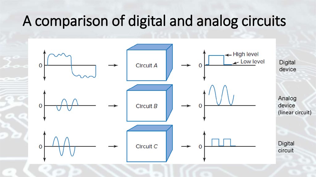
A comparison of digital and analog circuitsDigital
device
Analog
device
(linear circuit)
Digital
circuit
11.
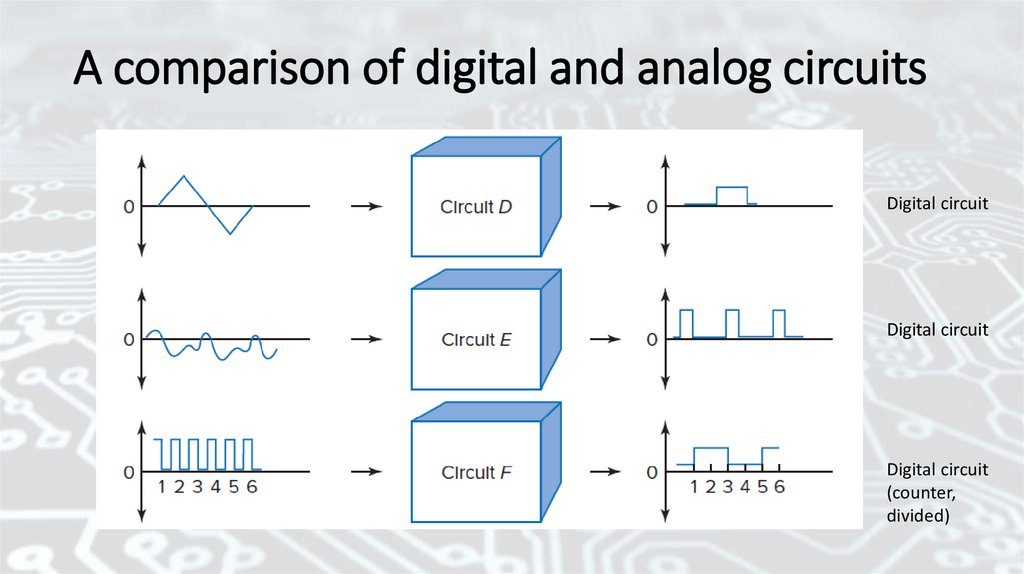
A comparison of digital and analog circuitsDigital circuit
Digital circuit
Digital circuit
(counter,
divided)
12.
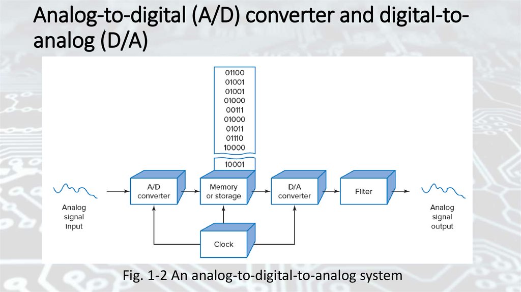
Analog-to-digital (A/D) converterRefer back to Fig. 1-2. The analog signal can be recreated by
sending the binary contents of memory to a digital-to-analog (D/A)
converter. The binary information is clocked out of memory at the
same rate as the original signal was sampled. Figure 1-4 shows the
output of the D/A converter. It can be seen that the waveform is not
exactly the same as the original analog signal. It is a series of discrete
steps. However, by using more steps, a much closer representation of
the original signal can be achieved. Step size is determined by the
number of binary digits (bits) used. The number of steps is found by
raising 2 to the power of the number of bits. A 5-bit system provides
25 = 32 steps, An 8-bit system would provide 28 = 256 steps.
13.
Analog-to-digital (A/D) converter and digital-toanalog (D/A)Fig. 1-2 An analog-to-digital-to-analog system
14.
Analog-to-digital (A/D) converter and digital-toanalog (D/A)Fig. 1-3 An analog waveform
Fig. 1-4 Output of the D/A converter
15.
Digital-to-analog (D/A) converterFigure 1-2 shows a system that converts an analog signal to
digital and then back to analog. An analog-to-digital (A/D) converter
is a circuit that produces a binary (only 0s and 1s) output. Note that
the numbers stored in memory are binary. A clock (a timing circuit)
drives the A/D converter to sample the analog signal on a repetitive
basis. Figure 1-3 shows the analog waveform in greater detail. This
waveform is sampled by the A/D converter every 20 microseconds
(μs). Thus, over a period of 0.8 millisecond (ms), forty samples are
taken. The required sampling rate for any analog signal is a function
of the frequency of that signal. The higher the frequency of the
signal, the higher the sampling rate.
16.
Analog FunctionsAnalog circuits perform certain operations. These operations
are usually performed on signals. Signals are electrical quantities,
such as voltages or currents, that have some merit or use. For
example, a microphone converts a human voice into a small voltage
whose frequency and level change with time. This small voltage is
called an audio signal.
Analog electronic circuits are often named after the function or
operation they provide. Amplification is the process of making a
signal larger or stronger, and circuits that do this are called
amplifiers.
17.
Analog Functions (1)Here is a list of the major types of analog electronic circuits:
1. Adders: Circuits that add signals together. Subtractors, also called
difference amplifiers, are also available.
2. Amplifiers: Circuits that increase signal voltage, current, or
power.
3. Attenuators: Circuits that decrease signal levels.
4. Clippers: Devices that prevent signals from exceeding a fixed
amplitude limit or limits.
5. Comparators: Devices that compare signal voltage to a reference
voltage. Some have one threshold voltage, and others have two.
18.
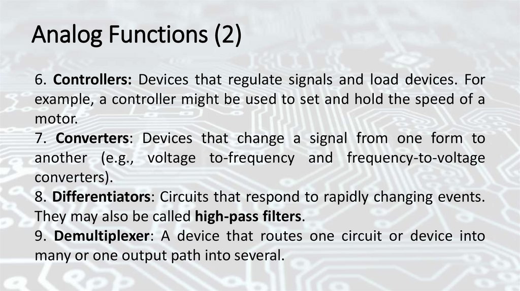
Analog Functions (2)6. Controllers: Devices that regulate signals and load devices. For
example, a controller might be used to set and hold the speed of a
motor.
7. Converters: Devices that change a signal from one form to
another (e.g., voltage to-frequency and frequency-to-voltage
converters).
8. Differentiators: Circuits that respond to rapidly changing events.
They may also be called high-pass filters.
9. Demultiplexer: A device that routes one circuit or device into
many or one output path into several.
19.
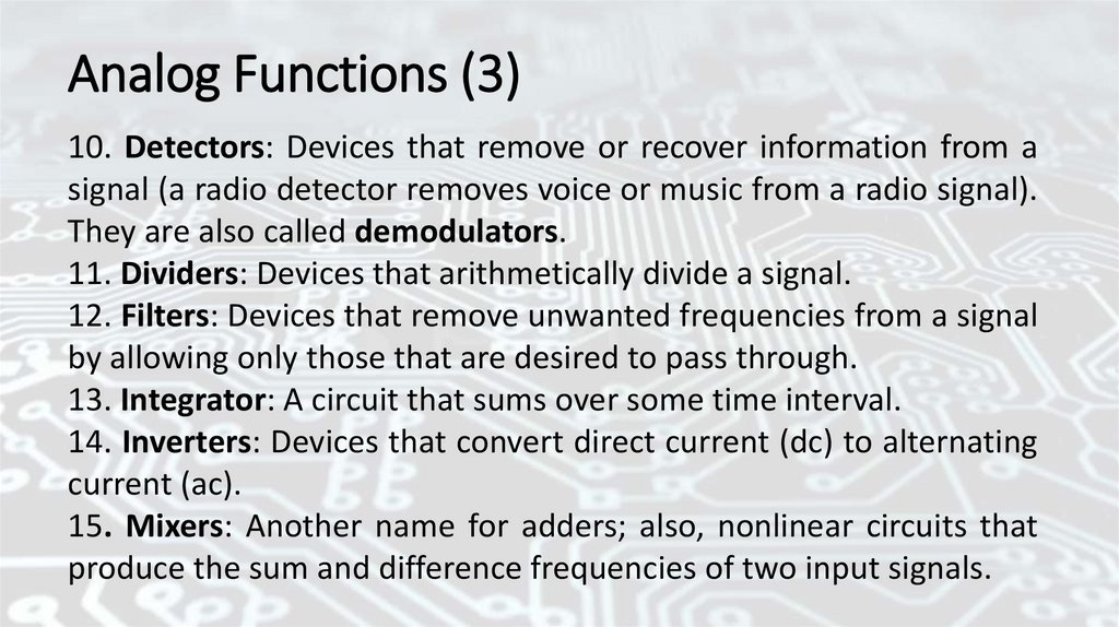
Analog Functions (3)10. Detectors: Devices that remove or recover information from a
signal (a radio detector removes voice or music from a radio signal).
They are also called demodulators.
11. Dividers: Devices that arithmetically divide a signal.
12. Filters: Devices that remove unwanted frequencies from a signal
by allowing only those that are desired to pass through.
13. Integrator: A circuit that sums over some time interval.
14. Inverters: Devices that convert direct current (dc) to alternating
current (ac).
15. Mixers: Another name for adders; also, nonlinear circuits that
produce the sum and difference frequencies of two input signals.
20.
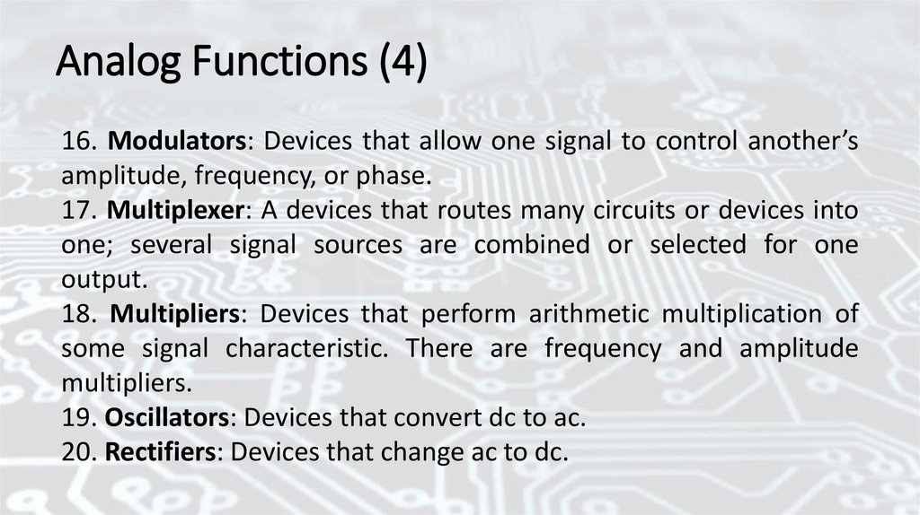
Analog Functions (4)16. Modulators: Devices that allow one signal to control another’s
amplitude, frequency, or phase.
17. Multiplexer: A devices that routes many circuits or devices into
one; several signal sources are combined or selected for one
output.
18. Multipliers: Devices that perform arithmetic multiplication of
some signal characteristic. There are frequency and amplitude
multipliers.
19. Oscillators: Devices that convert dc to ac.
20. Rectifiers: Devices that change ac to dc.
21.
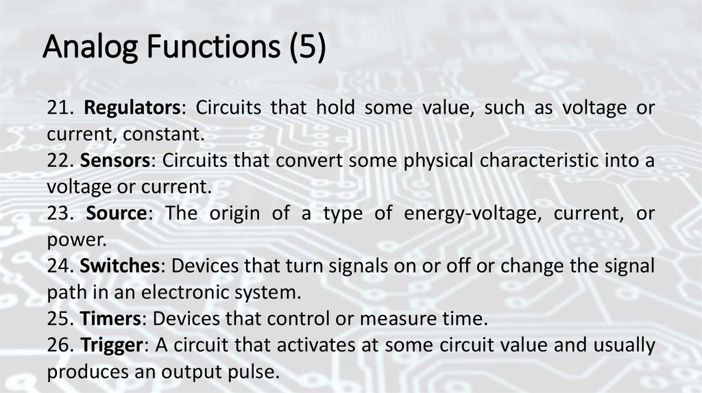
Analog Functions (5)21. Regulators: Circuits that hold some value, such as voltage or
current, constant.
22. Sensors: Circuits that convert some physical characteristic into a
voltage or current.
23. Source: The origin of a type of energy-voltage, current, or
power.
24. Switches: Devices that turn signals on or off or change the signal
path in an electronic system.
25. Timers: Devices that control or measure time.
26. Trigger: A circuit that activates at some circuit value and usually
produces an output pulse.
22.
Schematic & block diagramA schematic diagram shows all the individual parts of a
circuit and how they are interconnected. Schematics use
standard symbols to represent circuit components. A block
diagram shows all the individual functions of a system and how
the signals flow through the system. Schematic diagrams are
usually required for what is known as component-level
troubleshooting. A component is a single part, such as a
resistor, capacitor, or an integrated circuit. Component-level
repair requires the technician to isolate and replace individual
parts that are defective.
23.
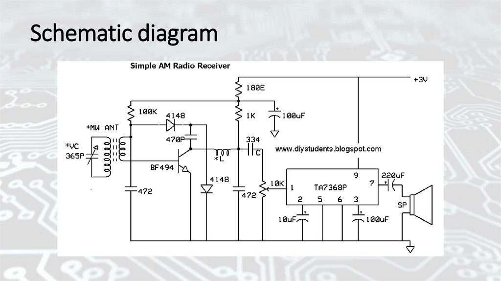
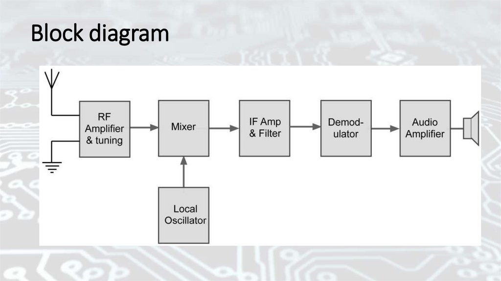
Schematic diagram24.
Block diagram25.
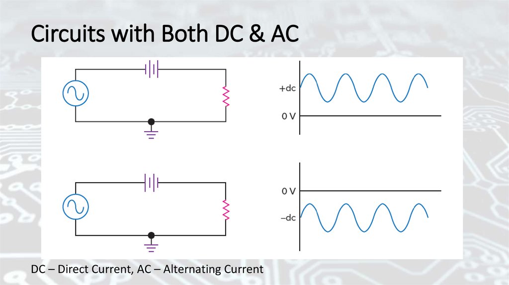
Circuits with Both DC & ACDC – Direct Current, AC – Alternating Current
26.
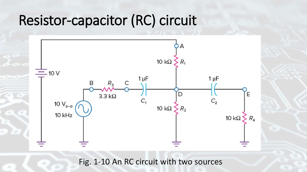
Resistor-capacitor (RC) circuitFig. 1-10 An RC circuit with two sources
27.
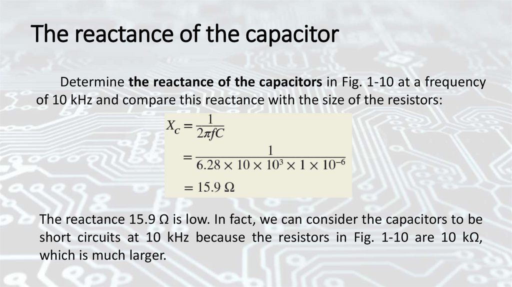
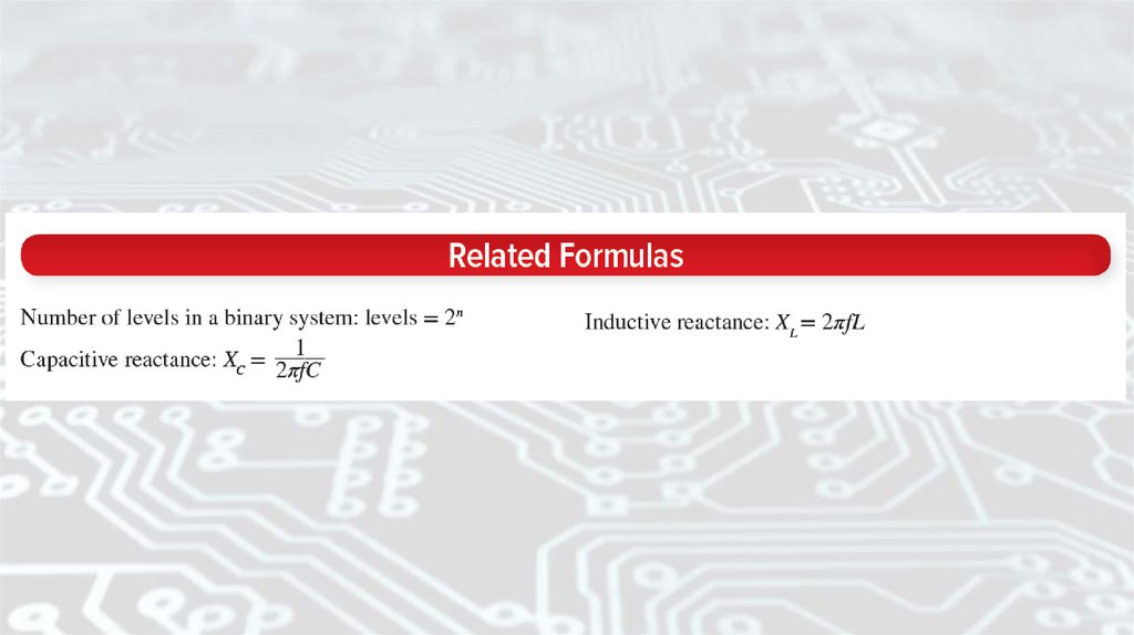
The reactance of the capacitorDetermine the reactance of the capacitors in Fig. 1-10 at a frequency
of 10 kHz and compare this reactance with the size of the resistors:
The reactance 15.9 Ω is low. In fact, we can consider the capacitors to be
short circuits at 10 kHz because the resistors in Fig. 1-10 are 10 kΩ,
which is much larger.
28.
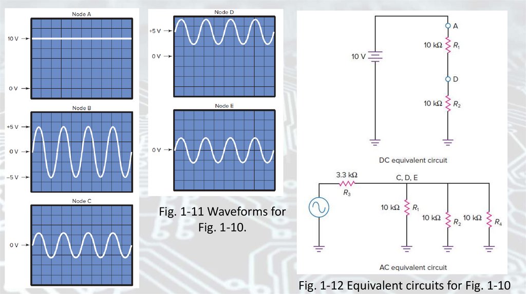
Fig. 1-11 Waveforms forFig. 1-10.
Fig. 1-12 Equivalent circuits for Fig. 1-10
29.
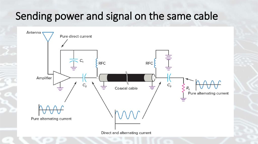
Sending power and signal on the same cable30.
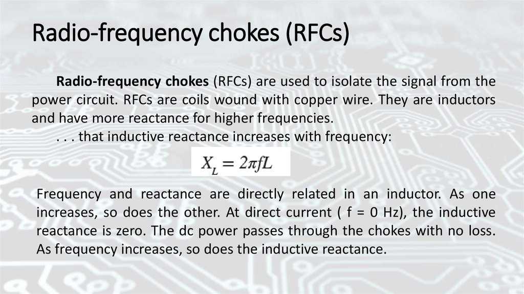
Radio-frequency chokes (RFCs)Radio-frequency chokes (RFCs) are used to isolate the signal from the
power circuit. RFCs are coils wound with copper wire. They are inductors
and have more reactance for higher frequencies.
. . . that inductive reactance increases with frequency:
Frequency and reactance are directly related in an inductor. As one
increases, so does the other. At direct current ( f = 0 Hz), the inductive
reactance is zero. The dc power passes through the chokes with no loss.
As frequency increases, so does the inductive reactance.
31.
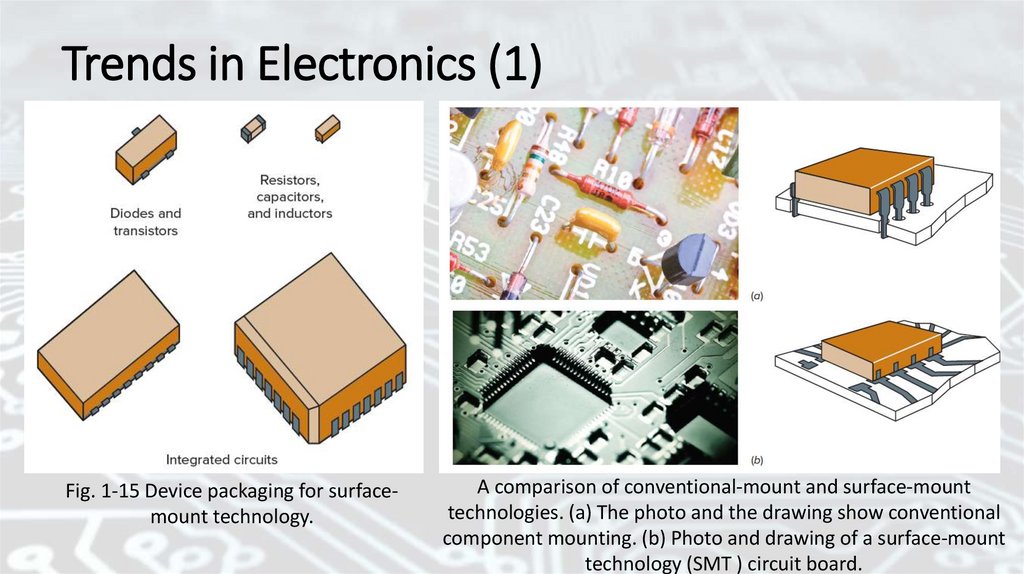
Trends in ElectronicsThe IC is the key to most electronic trends. These marvels of
microminiaturization keep expanding in performance and usually
decrease the cost of products. They also require less energy and offer high
reliability. One of the most popular ICs, the microprocessor, has created
many new products. DSP chips are now fast and inexpensive, encouraging
rapid growth.
Along with ICs, surface-mount technology (SMT) also helps to expand
electronics applications. The devices intended for SMT have a different
appearance.
32.
Trends in Electronics (1)Fig. 1-15 Device packaging for surfacemount technology.
A comparison of conventional-mount and surface-mount
technologies. (a) The photo and the drawing show conventional
component mounting. (b) Photo and drawing of a surface-mount
technology (SMT ) circuit board.
33.
34.
35.
Conductors & SemiconductorsToday, almost all electronic circuits are based on current flow in
semiconductors. The term “solid state” means that semiconducting
crystals are being used to get the job done. The mechanics of current flow
in semiconductors is different from that in conductors. Some current
carriers are not electrons. High temperatures create additional carriers in
semiconductors.
These
are
important
differences
between
semiconductors and conductors. The transistor is considered to be one of
the most important developments of all time. It is a semiconductor device.
Diodes and integrated circuits are also semiconductors.
36.
Nucleus, protons and neutron of atomsAll materials are made from atoms. At the center of any atom is a small,
dense core called the nucleus. Figure 2-1(a) shows that the nucleus of a copper
atom is made up of positive (+) particles called protons and neutral (N)
particles called neutrons. Around the nucleus are orbiting electrons that are
negative (−) particles. Copper, like all atoms, has an equal number of protons
and electrons. Thus, the net atomic charge is zero.
In electronics, the main interest is in the orbit that is farthest away from the
nucleus. It is called the valence orbit. In the case of copper, there is only one
valence electron. A copper atom can be simplified as shown in Fig. 2-1(b). Here,
the nucleus and the first three orbits are combined into a net positive (+)
charge. This is balanced by the single valence electron.
37.
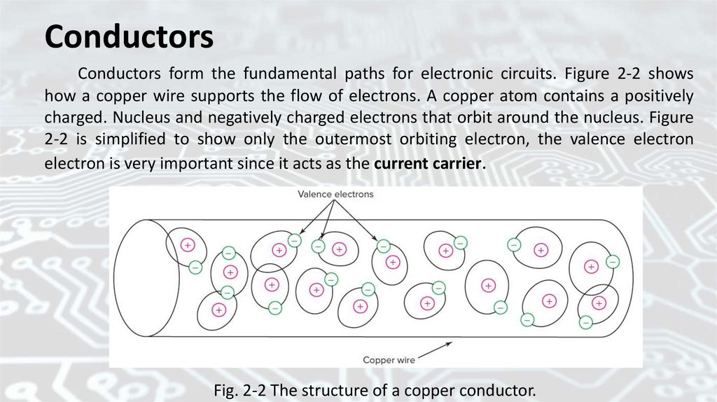
ConductorsConductors form the fundamental paths for electronic circuits. Figure 2-2 shows
how a copper wire supports the flow of electrons. A copper atom contains a positively
charged. Nucleus and negatively charged electrons that orbit around the nucleus. Figure
2-2 is simplified to show only the outermost orbiting electron, the valence electron
electron is very important since it acts as the current carrier.
Fig. 2-2 The structure of a copper conductor.
38.
Conductors (1)Even a very small copper wire contains billions of atoms, each with one
valence electron. These electrons are only weakly attracted to the nuclei of
the atoms. They are very easy to move. If an electromotive force (a voltage)
is applied across the wire, the valence electrons will respond and begin
drifting toward the positive end of the source voltage. Since there are so
many valence electrons and since they are so easy to move, we can expect
tremendous numbers of electrons to be set in motion by even a small
voltage. Thus, copper is an excellent electric conductor. It has very low
resistance.
39.
Positive temperature coefficientHeating a copper wire will change its resistance. As the wire becomes
warmer, the valence electrons become more active. They move farther
away from their nuclei, and they move more rapidly. This activity increases
the chance for collisions as current-carrying electrons drift toward the
positive end of the wire. These collisions absorb energy and increase the
resistance to current flow. The resistance of the wire increases as it is
heated. All conductors show this effect. As they become hotter, they
conduct less efficiently, and their resistance increases. Such materials are
said to have a positive temperature coefficient.
40.
SuperconductorsSuperconductivity is a set of physical properties observed in
certain materials where electrical resistance vanishes and
magnetic fields are expelled from the material. Any material
exhibiting these properties is a superconductor. Unlike an
ordinary metallic conductor, whose resistance decreases
gradually as its temperature is lowered, even down to near
absolute zero, a superconductor has a characteristic critical
temperature below which the resistance drops abruptly to zero.
41.
Copper, AluminumCopper is the most widely applied conductor in electronics.
Most of the wire used in electronics is made from copper.
Printed circuits use copper foil to act as circuit conductors.
Copper is a good conductor, and it is easy to solder. This makes
it very popular.
Aluminum is a good conductor, but not as good as copper. It
is used more in power transformers and transmission lines than
it is in electronics. Aluminum is less expensive than copper, but
it is difficult to solder and tends to corrode rapidly when
brought into contact with other metals.
42.
Silver, GoldSilver is the best conductor because it has the least
resistance. It is also easy to solder. The high cost of silver makes
it less widely applied than copper. However, silver-plated
conductors are sometimes used in critical electronic circuits to
minimize resistance.
Gold is a good conductor. It is very stable and does not
corrode as badly as copper and silver. Some sliding and moving
electronic contacts are gold-plated. This makes the contacts very
reliable.
43.
InsulatorThe opposite of a conductor is called an insulator. In an
insulator, the valence electrons are tightly bound to their parent
atoms. They are not free to move, so little or no current flows
when a voltage is applied. Practically all insulators used in
electronics are based on compounds.
A compound is a combination of two or more different kinds
of atoms. Some of the widely applied insulating materials
include rubber, plastic, Mylar, ceramic, Teflon, and polystyrene.
44.
SemiconductorsSemiconductors do not allow current to flow as easily as
conductors do. Under some conditions semiconductors can
conduct so poorly that they behave as insulators.
Silicon is the most widely used semiconductor material. It is
used to make diodes, transistors, and integrated circuits. These
and other components make modern electronics possible. It is
important to understand some of the details about silicon.
45.
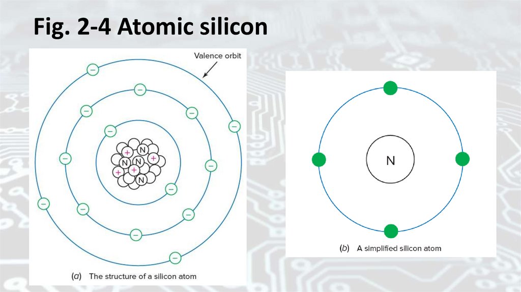
Atomic structure of siliconeFigure 2-4 shows atomic silicon. The compact bundle of
particles in the center of the atom [Fig. 2-4(a)] contains protons
and neutrons. This bundle is called the nucleus of the atom. The
protons show a positive (+) electric charge, and the neutrons
show no electric charge (N). Negatively charged electrons travel
around the nucleus in orbits. The first orbit has two electrons.
The second orbit has eight electrons. The last, or outermost,
orbit has four electrons. The outermost or valence orbit is the
most important atomic feature in the electrical behavior of
materials.
46.
Fig. 2-4 Atomic silicon47.
Active materialsFigure 2-4(b) shows only the nucleus and the valence orbit of a
silicon atom. Remember that there are four electrons in the valence
orbit.
Materials with four valence electrons are not stable. They tend to
combine chemically with other materials. They can be called active
materials. This activity can lead them to a more stable state. A law of
nature makes certain materials tend to form combinations that will
make eight electrons available in the valence orbit. Eight is an important
number because it gives stability.
48.
Silicon dioxideOne possibility is for silicon to combine with oxygen. A single silicon
atom can join, or link, with two oxygen atoms to form silicon dioxide
(SiO2). This linkage is called an ionic bond. The new structure, SiO2, is
much more stable than either silicon or oxygen. It is interesting to
consider that chemical, mechanical, and electrical properties often run
parallel. Silicon dioxide is stable chemically. It does not react easily with
other materials. It is also stable mechanically. It is a hard, glasslike
material. Finally, it is stable electrically. It does not conduct; in fact, it is
used as an insulator in integrated circuits and other solid-state devices.
SiO2 insulates because all of the valence electrons are tightly locked into
the ionic bonds. They are not easy to move and therefore do not
support the flow of current.
49.
Covalent bondingSometimes oxygen or another material is not available for silicon to
combine with. The silicon still wants the stability given by eight valence
electrons. If the conditions are right, silicon atoms will arrange to share
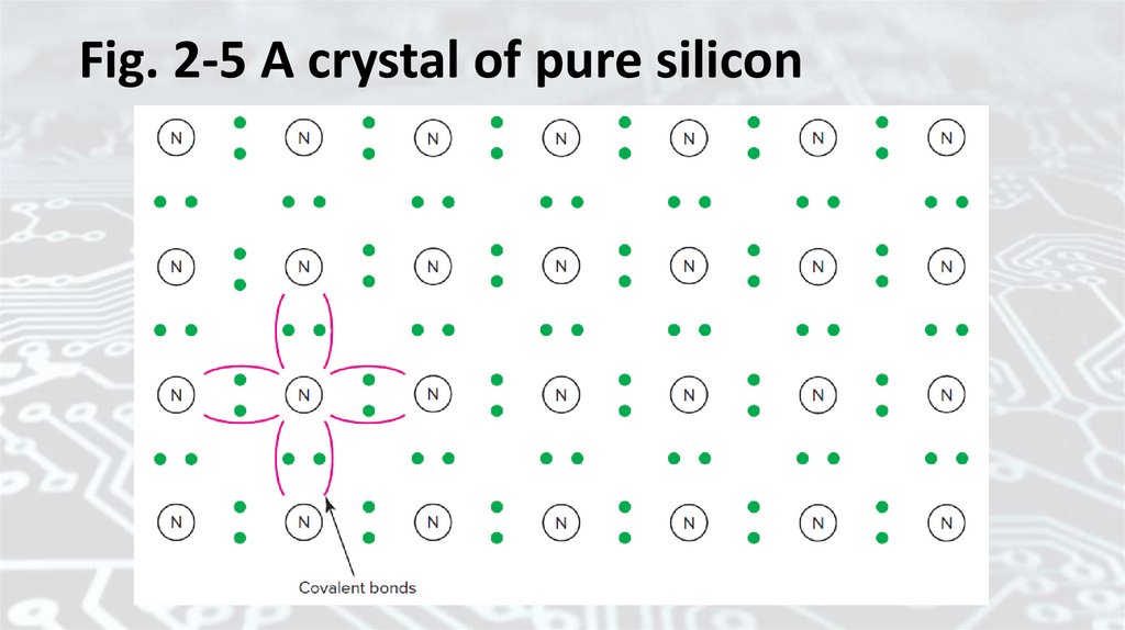
valence electrons. This process of sharing is called covalent bonding.
The structure that results is called a crystal. Figure 2-5 is a symbolic
diagramof a crystal of pure silicon. The dots represent valence electrons.
50.
Fig. 2-5 A crystal of pure silicon51.
Intrinsic siliconPure silicon crystals behave like insulators. Yet silicon itself is
classified as a semiconductor. Pure silicon is sometimes called intrinsic
silicon. Intrinsic silicon contains very few free electrons to support the
flow of current and therefore acts as an insulator.
Crystalline silicon can be made to semiconduct. One way to improve
its conduction is to heat it. Heat is a form of energy. A valence electron
can absorb some of this energy and move to a higher orbit level. The
high-energy electron has broken its covalent bond. Figure 2-6 shows a
high-energy electron in a silicon crystal. This electron may be called a
thermal carrier. It is free to move, so it can support the flow of current.
Now, if a voltage is placed across the crystal, current will flow.
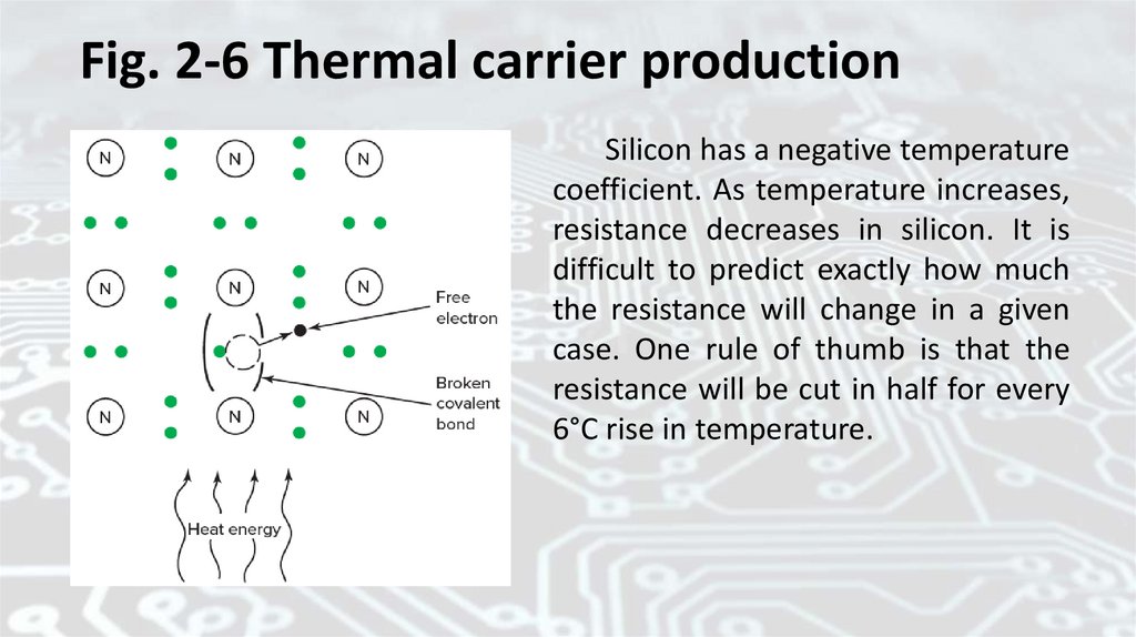
52.
Fig. 2-6 Thermal carrier productionSilicon has a negative temperature
coefficient. As temperature increases,
resistance decreases in silicon. It is
difficult to predict exactly how much
the resistance will change in a given
case. One rule of thumb is that the
resistance will be cut in half for every
6°C rise in temperature.
53.
GermaniumThe semiconductor material germanium is used to make transistors
and diodes, too. Germanium has four valence electrons and can form
the same type of crystalline structure as silicon. It is interesting to
observe that the first transistors were all made of germanium. The first
silicon transistor was not developed until 1954. Now silicon has almost
entirely replaced germanium. One of the major reasons for this shift
from germanium to silicon is the temperature response. Germanium
also has a negative temperature coefficient. The rule of thumb for
germanium is that the resistance will be cut in half for every 10°C rise in
temperature. This would seem to make germanium more stable with
temperature change.
54.
Difference between Germanium and SiliconeThe big difference between germanium and silicon is the amount of
heat energy needed to move one of the valence electrons to a higher
orbit level, breaking its covalent bond. This is far easier to do in a
germanium crystal. The silicon crystal will actually have 1,000 times the
resistance of the germanium crystal. So even though the resistance of
silicon drops more rapidly than that of germanium with increasing
temperature, silicon is still going to show greater resistance than
germanium at a given temperature.
Germanium started the solid-state revolution in electronics, but
silicon has taken over. The integrated circuit is a key part of most
electronic equipment today. It is not practical to make integrated circuits
from germanium, but silicon works well in this application.
55.
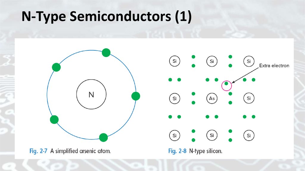
N-Type SemiconductorsDoping is a process of adding other materials called impurities to
the silicon crystal to change its electrical characteristics. One such
impurity material is arsenic. Arsenic is known as a donor impurity
because each arsenic atom donates one free electron to the crystal.
Figure 2-7 shows a simplified arsenic atom. Arsenic is different from
silicon in several ways, but the important difference is in the valence
orbit. Arsenic has five valence electrons.
When an arsenic atom enters a silicon crystal, a free electron will
result. Figure 2-8 shows Doping Arsenic what happens. Since electrons
have a negative charge, we say that an N-type semiconductor material
results.
56.
N-Type Semiconductors (1)57.
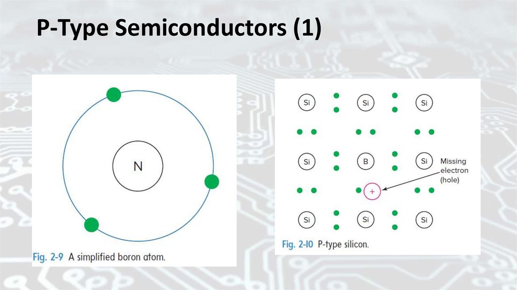
P-Type SemiconductorsDoping can involve the use of other kinds of impurity materials.
Figure 2-9 shows a simplified boron atom. Note that boron has only
three valence electrons. If a boron atom enters the silicon crystal,
another type of current carrier will result. Figure 2-10 shows that
one of the covalent bonds with neighboring silicon atoms cannot be
formed. This produces a hole, or missing electron. The hole is
assigned a positive charge since it is capable of attracting, or being
filled by, an electron. Holes serve as current carriers. Boron is known
as an acceptor impurity. Each boron atom in the crystal will create a
hole that is capable of accepting an electron. We say that an P-type
semiconductor material results.
58.
P-Type Semiconductors (1)59.
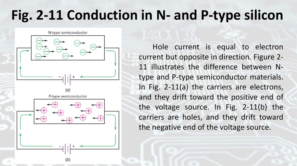
Fig. 2-11 Conduction in N- and P-type siliconHole current is equal to electron
current but opposite in direction. Figure 211 illustrates the difference between Ntype and P-type semiconductor materials.
In Fig. 2-11(a) the carriers are electrons,
and they drift toward the positive end of
the voltage source. In Fig. 2-11(b) the
carriers are holes, and they drift toward
the negative end of the voltage source.
60.
Majority and Minority CarriersWhen N- and P-type semiconductor materials are made, the doping
levels can be as small as 1 part per million or 1 part per billion. Only a tiny
trace of impurity materials having five or three valence electrons enters the
crystal. It is not possible to make the silicon crystal absolutely pure. Thus, it
is easy to imagine that an occasional atom with three valence electrons
might be present in an N-type semiconductor. An unwanted hole will exist
in the crystal. This hole is called a minority carrier. The free electrons are
the majority carriers.
In a P-type semiconductor, one expects holes to be the carriers. They
are in the majority. A few free electrons might also be present. They will be
the minority carriers in this case.
61.
Compound semiconductorsThe following is a partial list of compound semiconductors:
Gallium arsenide;
Indium phosphide;
Mercury cadmium telluride;
Silicon carbide;
Cadmium sulfide;
Cadmium telluride.
62.
Compound semiconductorsThe following is a partial list of compound semiconductors:
Gallium arsenide;
Indium phosphide;
Mercury cadmium telluride;
Silicon carbide;
Cadmium sulfide;
Cadmium telluride.
63.
Other Semiconductor MaterialsWhat is needed is a way to have higher carrier mobility, that
is, get the holes and electrons to move faster. Mobility can be
improved by using other materials, such as gallium arsenide. You
might have run across the term GASFET, which is an acronym for
gallium arsenide field effect transistor. GASFETs are used in very
high-frequency applications.
Carrier mobility can also be improved by using a variety of
new silicon technologies, including strained silicon, silicon
germanium (SiGe), and silicon on insulator (SOI), as well as
combinations of these materials. And also, silicon carbide devices
can safely handle thousands of volts.
64.
Other Semiconductor Materials (1)Another promising
development
is
the organic
semiconductor. These devices use semiconducting and sometimes
conducting materials that are made of molecules containing
carbon, mostly in combination with hydrogen and oxygen. Slower
than silicon, but more flexible and potentially much cheaper,
organic electronics has already produced circuits with hundreds of
transistors printed on plastic, experimental sensors and
memories, and displays that bend like paper. Organic displays
might compete with liquid crystal displays, as they are brighter
and faster and don’t suffer from a limited viewing angle.
65.
Band GapsIn a semiconductor, such as silicon, the energy difference
between the top of the valence band and the bottom of the
conduction band is called the band gap. Or it is the amount of
energy, in electron volts (eV), required to free a valence electron
from its orbit and boost it to the conduction level.
1 eV = 1.602 × 10⁻¹⁹ joules
The joule is the SI unit of work or energy and amounts to a force
of 1 newton applied over a distance of 1 meter, or to a current of
1 ampere through a 1-ohm resistor for 1 second. The band gap for
silicon is 1.1 eV, and for gallium arsenide, it’s 1.43 eV.
66.
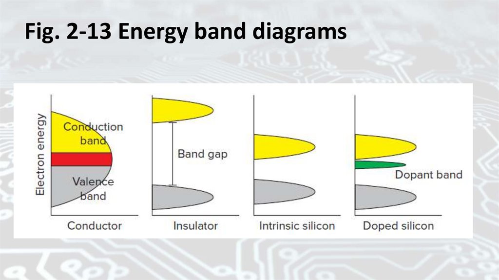
Fig. 2-13 Energy band diagrams67.
Photon energyThe photon energy of light varies according to the different
wavelengths of the light. The entire spectrum of sunlight, from
infrared to ultraviolet, covers a range from about 0.5 eV to about 2.9
eV. For example, red light has an energy of about 1.7 eV, and blue light
has an energy of about 2.7 eV. Most solar cells cannot use about 55
percent of the energy of sunlight, because this energy is either below
the band gap of the material or is excessive. There is currently intense
interest in finding new semiconductor materials to improve the
efficiency and lower the cost of solar cells. It is possible to stack cells
that have different band gaps to increase efficiency.
68.
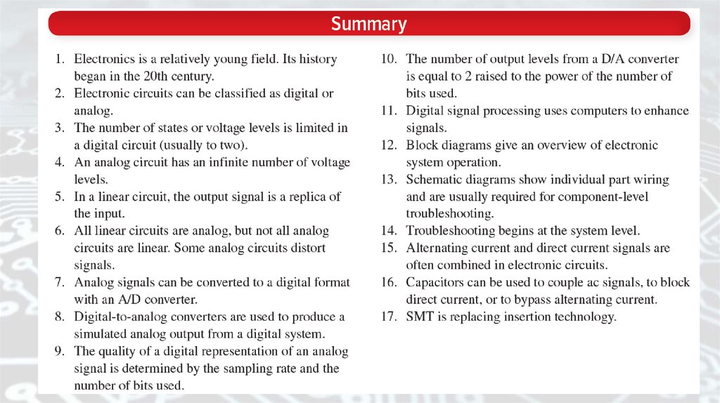
Summary1. Good conductors, such as copper, contain a large number of current
carriers.
2. In a conductor, the valence electrons are weakly attracted to the
nuclei of the atoms.
3. Heating a conductor will increase its resistance. This response is
called a positive temperature coefficient.
4. Silicon atoms have four valence electrons. They can form covalent
bonds that result in a stable crystal structure.
5. Heat energy can break covalent bonds, making free electrons
available to conduct current. This gives silicon and other
semiconductor materials a negative temperature coefficient.
69.
Summary (1)6. At room temperature, germanium crystals have 1,000 times more
thermal carriers than silicon crystals do. This makes germanium diodes
and
transistors less useful than silicon devices for many applications.
7. The process of adding impurities to a semiconductor crystal is called
doping.
8. Doping a semiconductor crystal changes its electrical characteristics.
9. Donor impurities have five valence electrons and produce free
electrons in the crystal. This forms N-type semiconductor material.
10. Free electrons serve as current carriers.
70.
Summary (2)11. Acceptor impurities have three valence electrons and produce
holes in the crystal.
12. Holes in semiconductor materials serve as current carriers.
13. Hole current is opposite in direction to electron current.
14. Semiconductors with free holes are classified as P-type materials.
15. Impurities with five valence electrons produce N-type
semiconductors.
16. Impurities with three valence electrons produce P-type
semiconductors.
71.
Summary (3)17. Holes drift toward the negative end of a voltage source.
18. Electrons are majority carriers for N-type material. Holes are
majority carriers for P-type material.
19. Holes are minority carriers for N-type material. Electrons are
minority carriers for P-type material.
20. The number of minority carriers increases with temperature.
21. To move a valence electron to the conduction band, an amount of
energy equal to or greater than the band gap must be applied.