 FOR TRANSMISSION ELECTRON MICROSCOPY (TEM)")


 chemistry
 electronics
Similar presentations:
 An introduction")
")


Cross-section sample preparation using focused ion beam system (FIB) for transmission electron microscopy (TEM)
1. CROSS-SECTION SAMPLE PREPARATION USING FOCUSED ION BEAM SYSTEM (FIB) FOR TRANSMISSION ELECTRON MICROSCOPY (TEM)
Speaker: Volochaev M.N.Scientific supervisor: Loginov Yu.Yu.
2.
What is TEM?What can be observed by TEM:
• Thin films and foils;
• meso- micro- and nanoparticles;
• biological specimens;
Basic requirements for TEM
specimens:
• specimen thickness max 0.1 um;
TEM Hitachi HT 7700
• Stability under the electron
beam and vacuum influence ;
3.
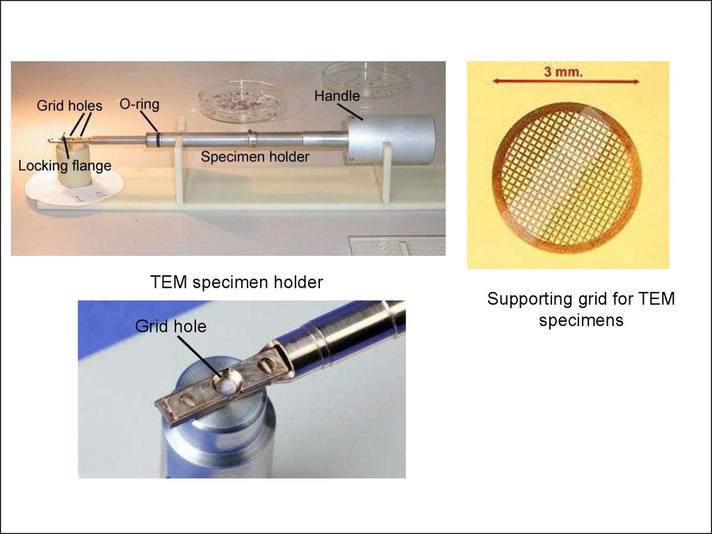
TEM specimen holderGrid hole
Supporting grid for TEM
specimens
4.
Examples500 nm
Ni-Ti thin foil
50 nm
Ni nanoparticles (catalysts) and carbon nanotubes
1 um
Co-Al2O3 thin film
Neonothopanus nambi (lat.) biological specimen
5.
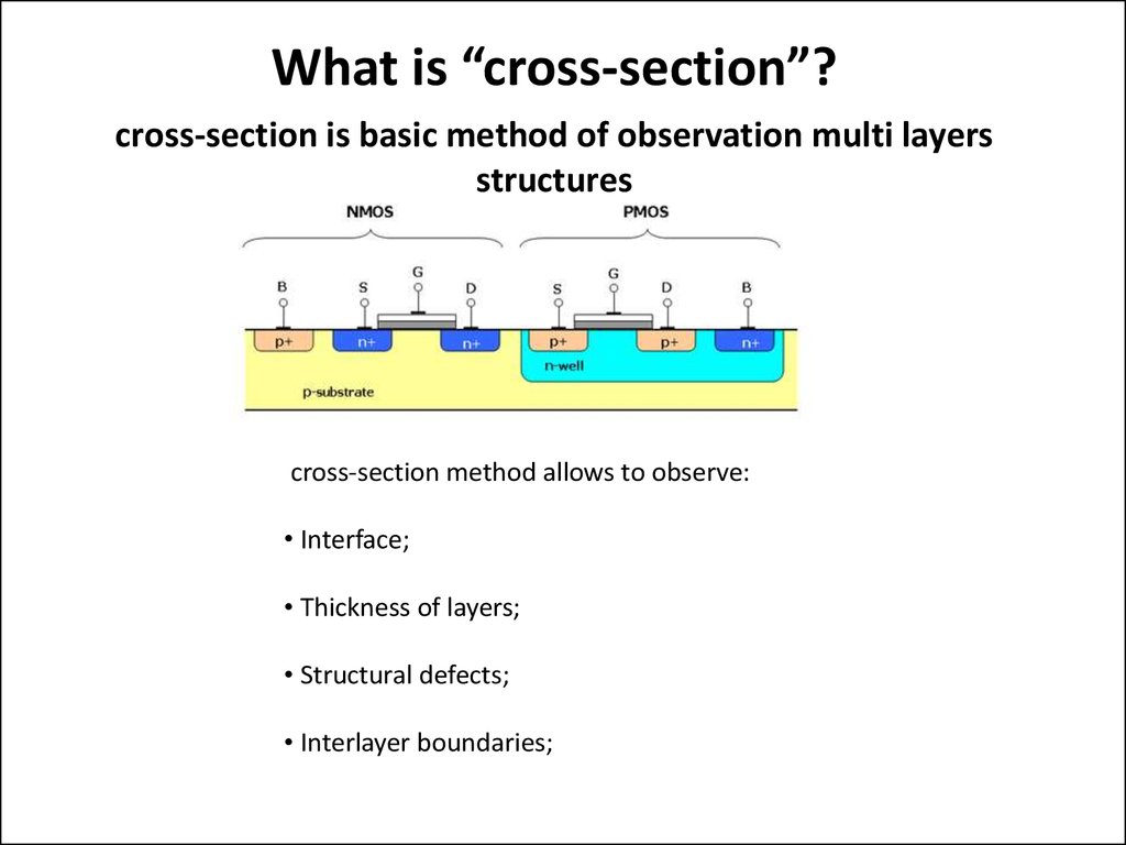
What is “cross-section”?cross-section is basic method of observation multi layers
structures
cross-section method allows to observe:
• Interface;
• Thickness of layers;
• Structural defects;
• Interlayer boundaries;
6.
Classic method of cross-sectionsample preparation
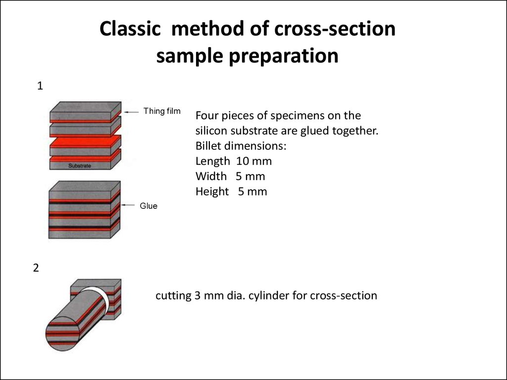
1
Thing film
Four pieces of specimens on the
silicon substrate are glued together.
Billet dimensions:
Length 10 mm
Width 5 mm
Height 5 mm
Glue
2
cutting 3 mm dia. cylinder for cross-section
7.
3sawing disc of 100 um thickness
4 Thinning the disk up to 10 microns
by Dimple Grinder System (Gatan)
8.
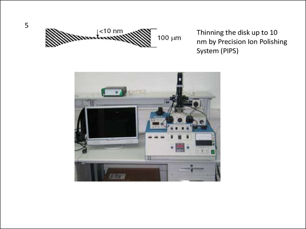
5Thinning the disk up to 10
nm by Precision Ion Polishing
System (PIPS)
9.
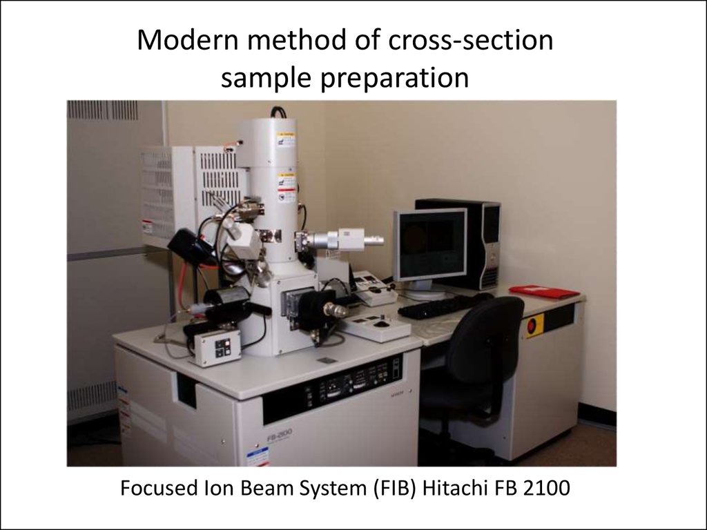
Modern method of cross-sectionsample preparation
Focused Ion Beam System (FIB) Hitachi FB 2100
10. Basic steps of cross-section sample preparation by FIB
1. Deposition of protective tungsten coating on the sample surface11.
2. Cutting half-finished (lamella)12.
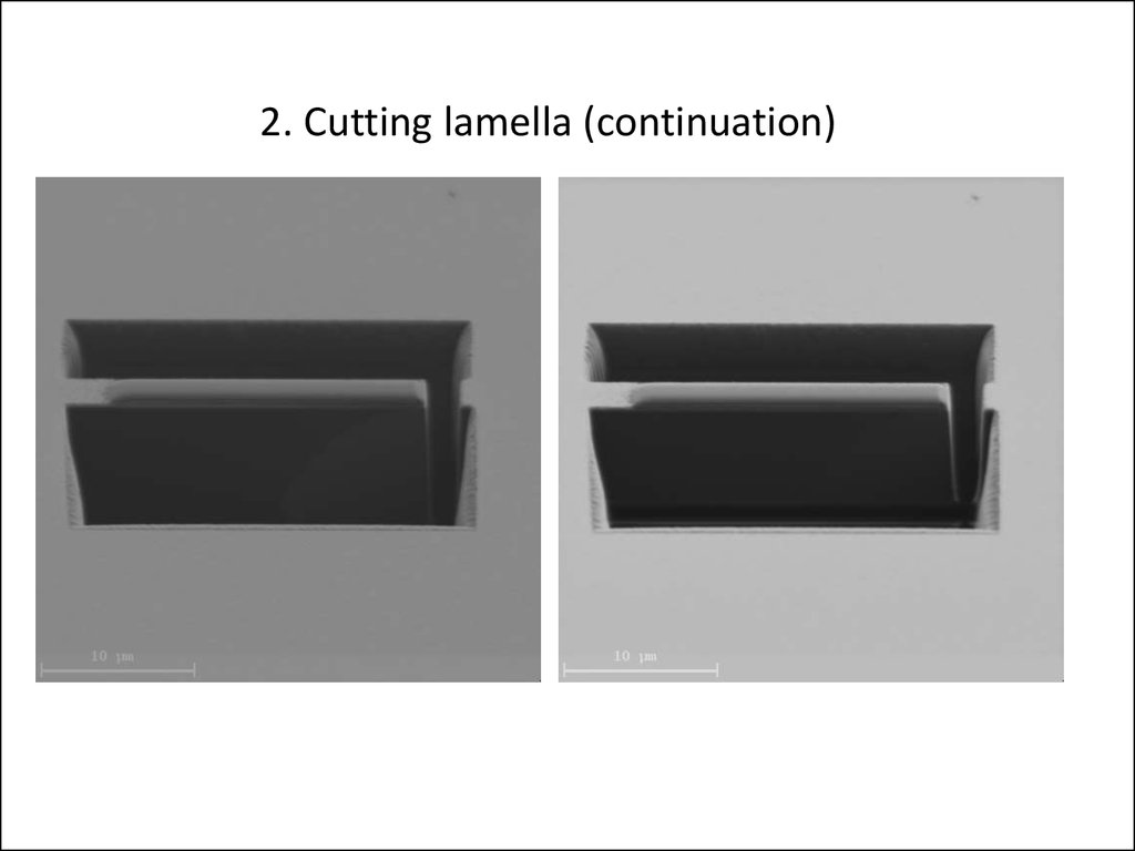
2. Cutting lamella (continuation)13.
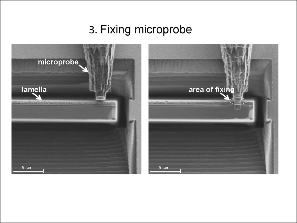
3. Fixing microprobemicroprobe
lamella
area of fixing
14.
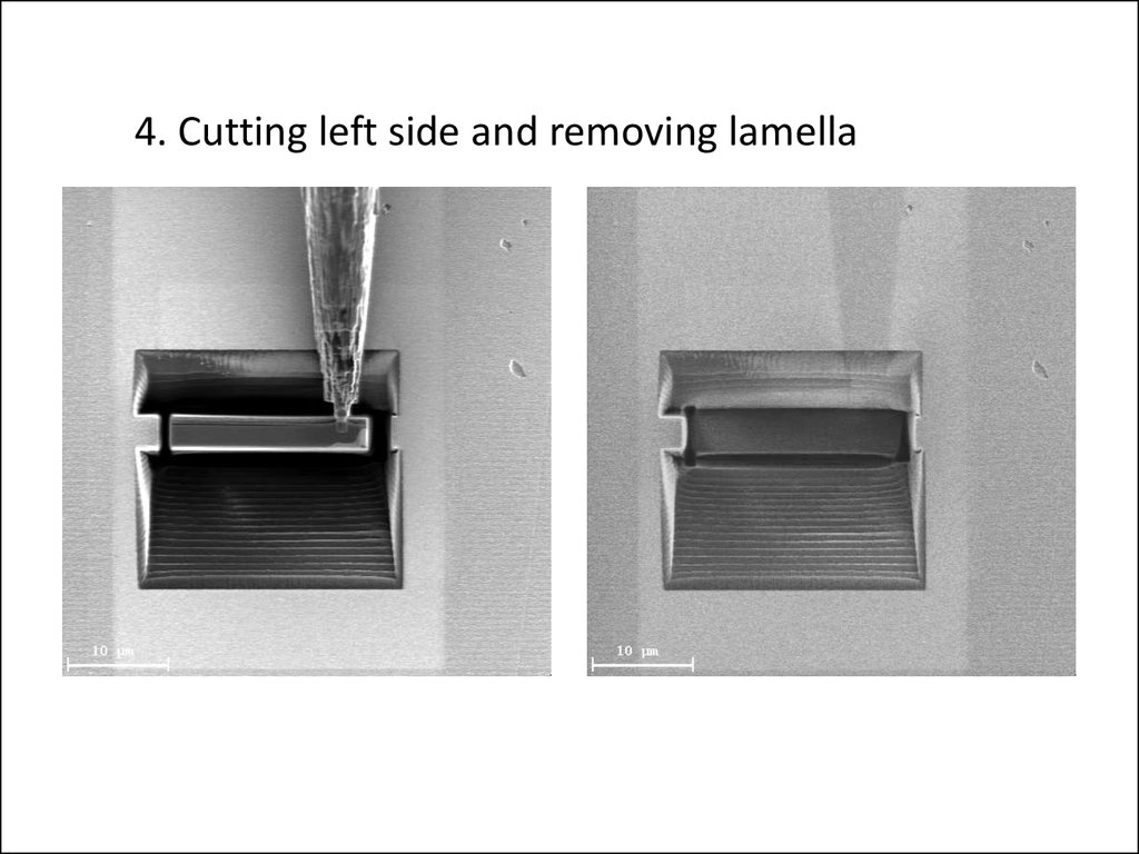
4. Cutting left side and removing lamella15.
5. Fixing lamella on the toothed semicirclelamella
16.
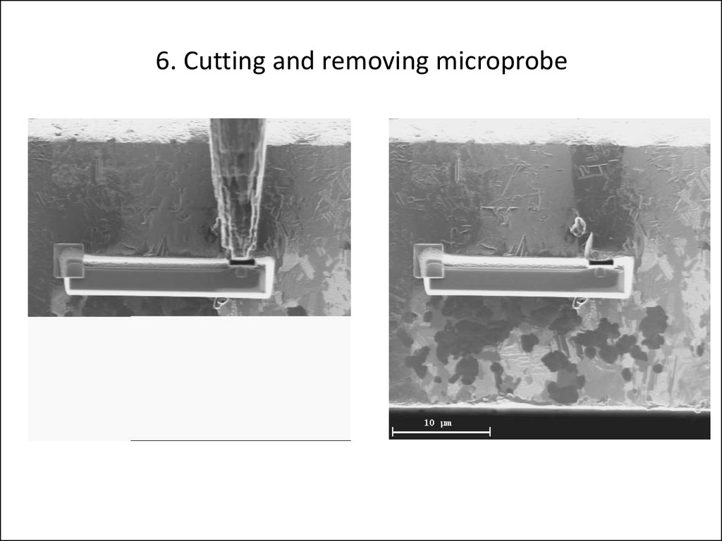
6. Cutting and removing microprobe17.
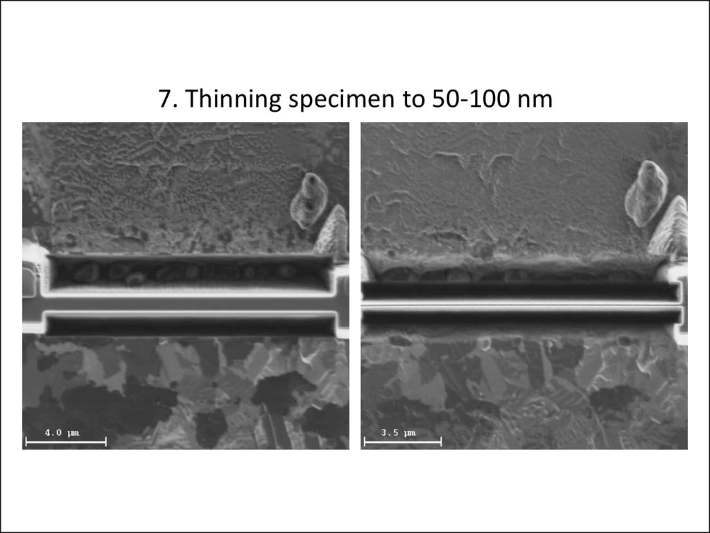
7. Thinning specimen to 50-100 nm18.
Finish resultОбласть просмотра в ПЭМ
Disadvantages of FIB method
1. Damaging top layer during deposition tungsten protective coating
2. It is impossible to prepare the sample with thickness less than 50 nm
19.
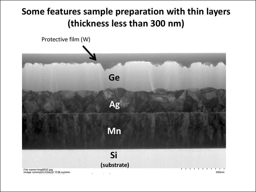
Some features sample preparation with thin layers(thickness less than 300 nm)
Protective film (W)
Ge
Ag
Mn
Si
(substrate)
20.
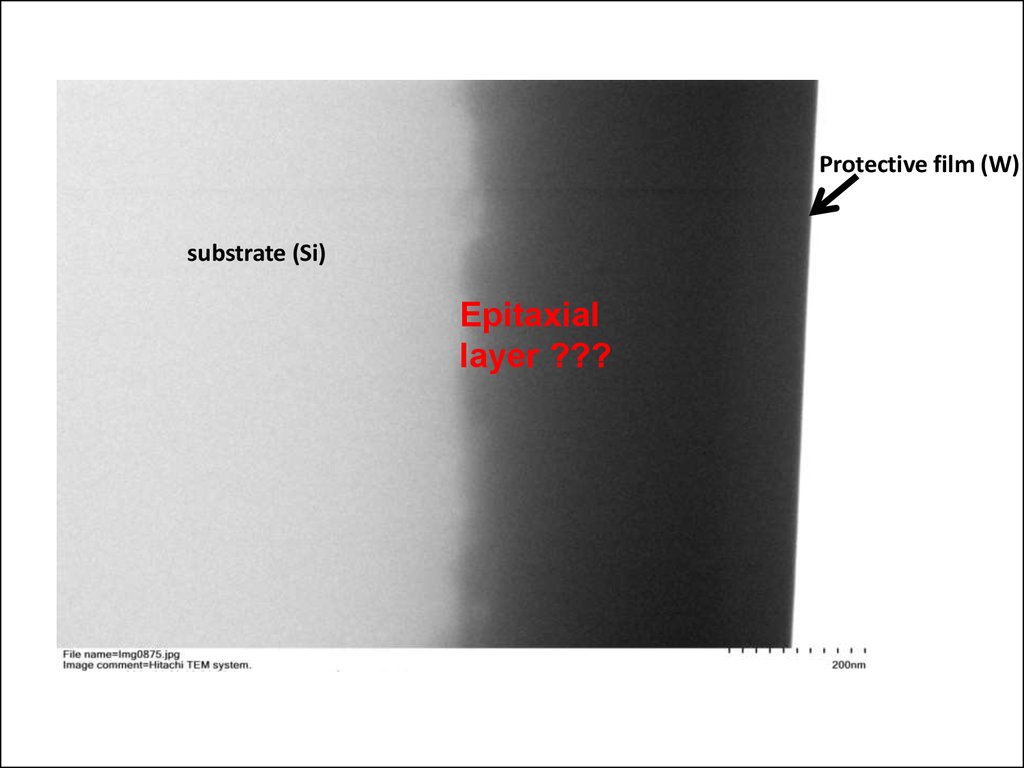
Protective film (W)substrate (Si)
Epitaxial
layer ???
21.
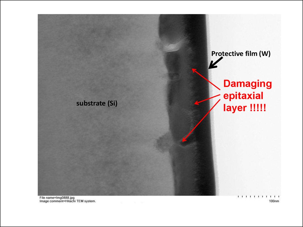
Protective film (W)substrate (Si)
Damaging
epitaxial
layer !!!!!
22.
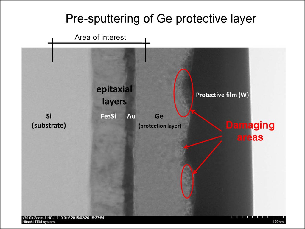
Pre-sputtering of Ge protective layerArea of interest
epitaxial
layers
Si
(substrate)
Fe3Si
Au
Protective film (W)
Ge
(protection layer)
Damaging
areas
23.
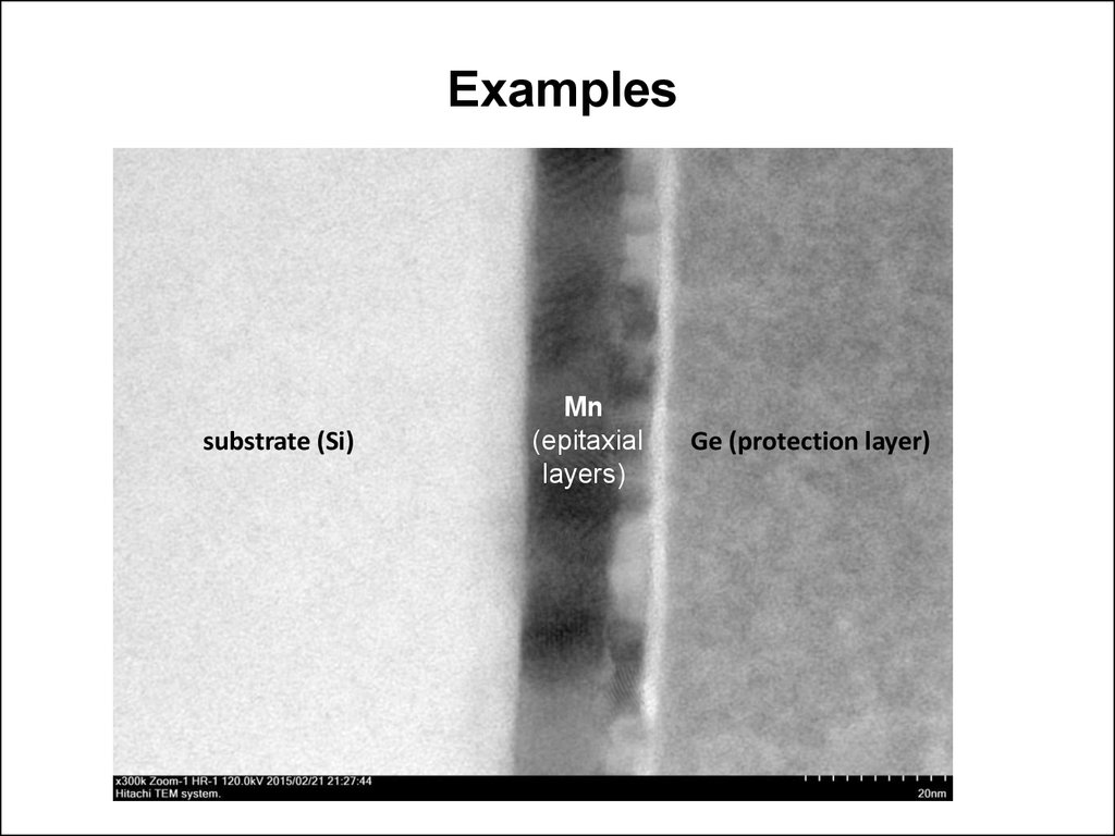
Examplessubstrate (Si)
Mn
(epitaxial
layers)
Ge (protection layer)
24.
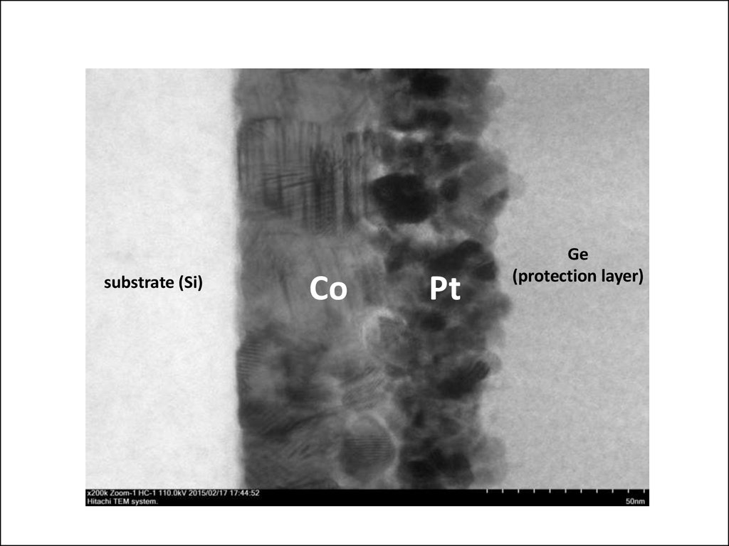
substrate (Si)Co
Pt
Ge
(protection layer)
25.
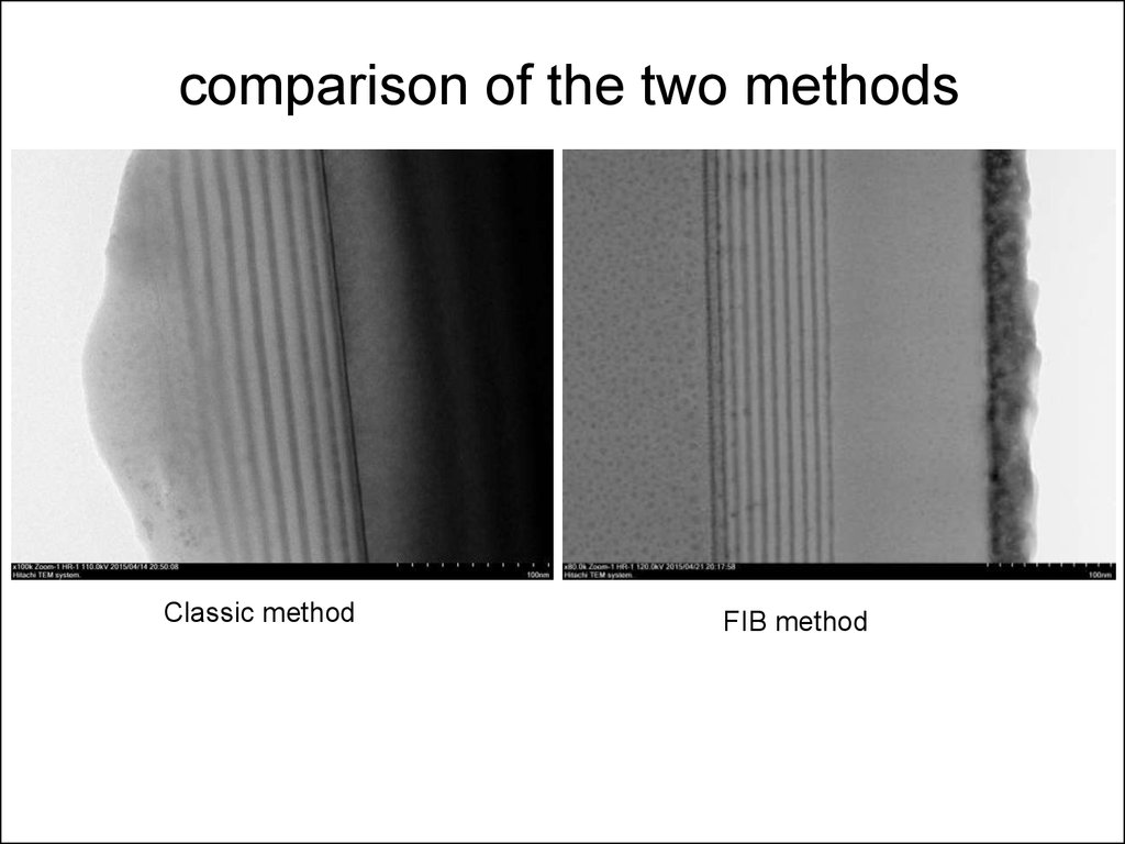
comparison of the two methodsClassic method
FIB method
26.
Thanks for yourattention!